
2016 Microchip Technology Inc.
DS20005543B-page 1
PL138-48
Features
• Four Differential 2.5V/3.3V LVPECL Output Pairs
• Output Frequency: ≤800 MHz
• Two Selectable Differential Input Pairs
• Translates Any Standard Single-Ended or
Differential Input Format to LVPECL Output. It
Can Accept the Following Standard Input Formats
and More:
- LVPECL, LVCMOS, LVDS, HCSL, SSTL,
LVHSTL, CML
• Output Skew: 25 ps (typ.)
• Part-to-Part Skew: 140 ps (typ.)
• Propagation Delay: 1.5 ns (typ.)
• Additive Jitter: <100 fs (max.)
• Operating Supply Voltage: 2.375V ~ 3.63V
• Operating Temperature Range from –40
°
C to
+85
°
C
• Package Availability: 16-Pin QFN and 20-Pin
TSSOP
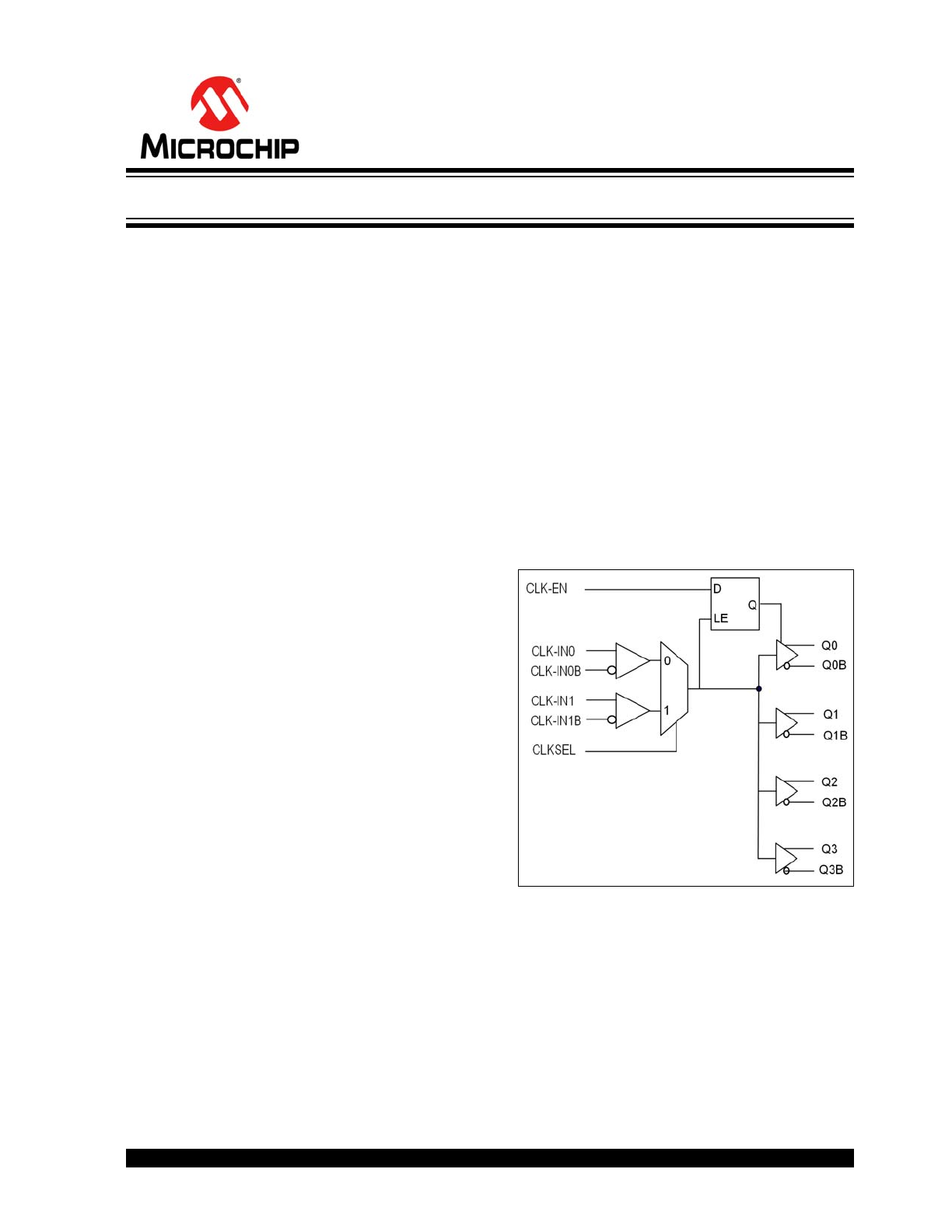
General Description
The PL138-48 is a high performance low-cost 1:4
outputs differential LVPECL fanout buffer.
Microchip’s family of differential LVPECL buffers are
designed to operate from a single power supply of 2.5V
±5% or 3.3V ±10%. The differential input pairs are
designed to accept most standard input signal levels,
using an appropriate resistor bias network, and
produce a high quality set of outputs with the lowest
possible skew on the outputs, which is guaranteed for
part-to-part or lot-to-lot skew.
Designed to fit in a small form-factor package, the
PL138-48 offers up to 800 MHz of output operation with
very low-power consumption and lowest additive jitter
of any comparable device.
Block Diagram
2.5V to 3.3V, Low-Skew, 1:4 Differential PECL Fanout Buffer
PL138-48
DS20005543B-page 2
2016 Microchip Technology Inc.
1.0
ELECTRICAL CHARACTERISTICS
Absolute Maximum Ratings †
Supply Voltage (V
DD
) ...............................................................................................................................................+4.6V
Input Voltage, DC (V
I
)..........................................................................................................................–0.5V to V
DD
+0.5V
Output Voltage, DC (V
O
) .....................................................................................................................–0.5V to V
DD
+0.5V
ESD Protection (HBM) ...............................................................................................................................................2 kV
† Notice: Stresses above those listed under “Absolute Maximum Ratings” may cause permanent damage to the device.
This is a stress rating only and functional operation of the device at those or any other conditions above those indicated
in the operational sections of this specification is not intended. Exposure to maximum rating conditions for extended
periods may affect device reliability.
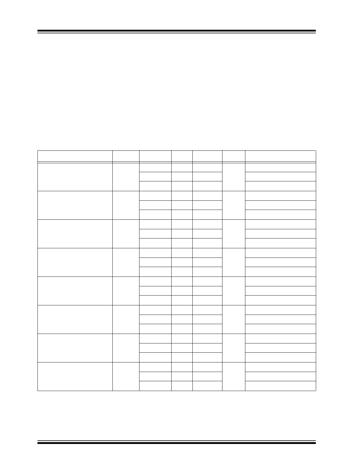
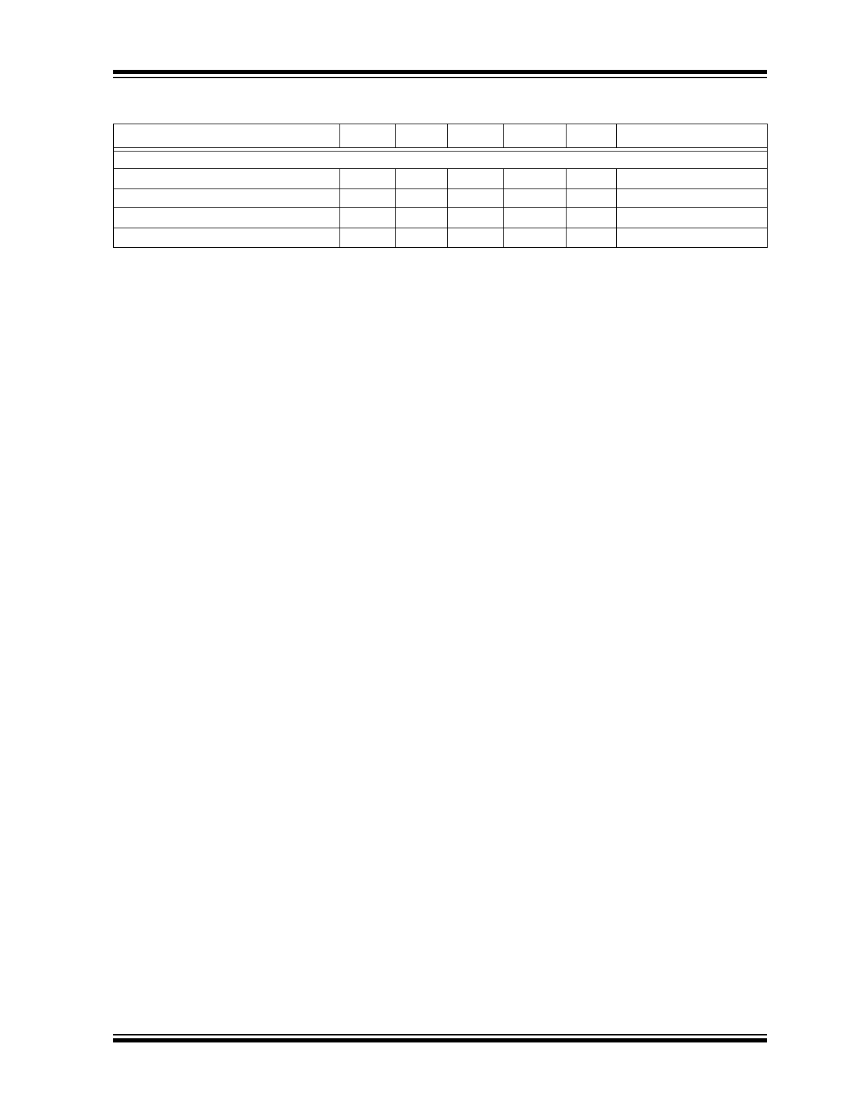
DC ELECTRICAL CHARACTERISTICS
Specifications: V
CC
= 3.3V; V
EE
= 0V. Input and output parameters vary 1:1 with V
CC
when V
CC
varies ±10%.
Parameters
Symbol
Min.
Typ.
Max.
Units
Conditions
Output High Voltage, (
Note 1
)
V
OH
2.215
2.320
2.420
V
At –40°C
2.275
2.350
2.420
At +25°C
2.275
2.350
2.420
At +85°C
Output Voltage Low, (
Note 1
)
V
OL
1.470
1.610
1.745
V
At –40°C
1.490
1.585
1.680
At +25°C
1.490
1.585
1.680
At +85°C
Input High Voltage
V
IH
2.075
—
2.420
V
At –40°C
2.135
—
2.420
At +25°C
2.135
—
2.420
At +85°C
Input Low Voltage
V
IL
1.470
—
1.890
V
At –40°C
1.490
—
1.825
At +25°C
1.490
—
1.825
At +85°C
Output Voltage Reference,
(
Note 2
)
V
BB
1.86
—
1.98
V
At –40°C
1.92
—
2.04
At +25°C
1.92
—
2.04
At +85°C
Input High Voltage Common
Mode Range, (
Note 3
,
Note 4
)
V
CMR
1.2
—
3.3
V
At –40°C
1.2
—
3.3
At +25°C
1.2
—
3.3
At +85°C
Input High Current, (
Note 5
)
I
IH
—
—
75
µA
At –40°C
—
—
75
At +25°C
—
—
75
At +85°C
Input Low Current, (
Note 5
)
I
IL
–75
—
—
µA
At –40°C
–75
—
—
At +25°C
–75
—
—
At +85°C
Note 1: Outputs terminated with 50Ω to V
CCO
–2V.
2: Single-ended input operation is limited to VCC ≥ 3V in LVPECL mode.
3: Common mode voltage is defined as V
IH
.
4: For single-ended applications, the maximum input voltage for CLK-INx, CLK-INxB is V
CC
+0.3V.
5: CLK-IN0, CLK-IN1; CLK-IN0B, CLK-IN1B.
2016 Microchip Technology Inc.
DS20005543B-page 3
PL138-48
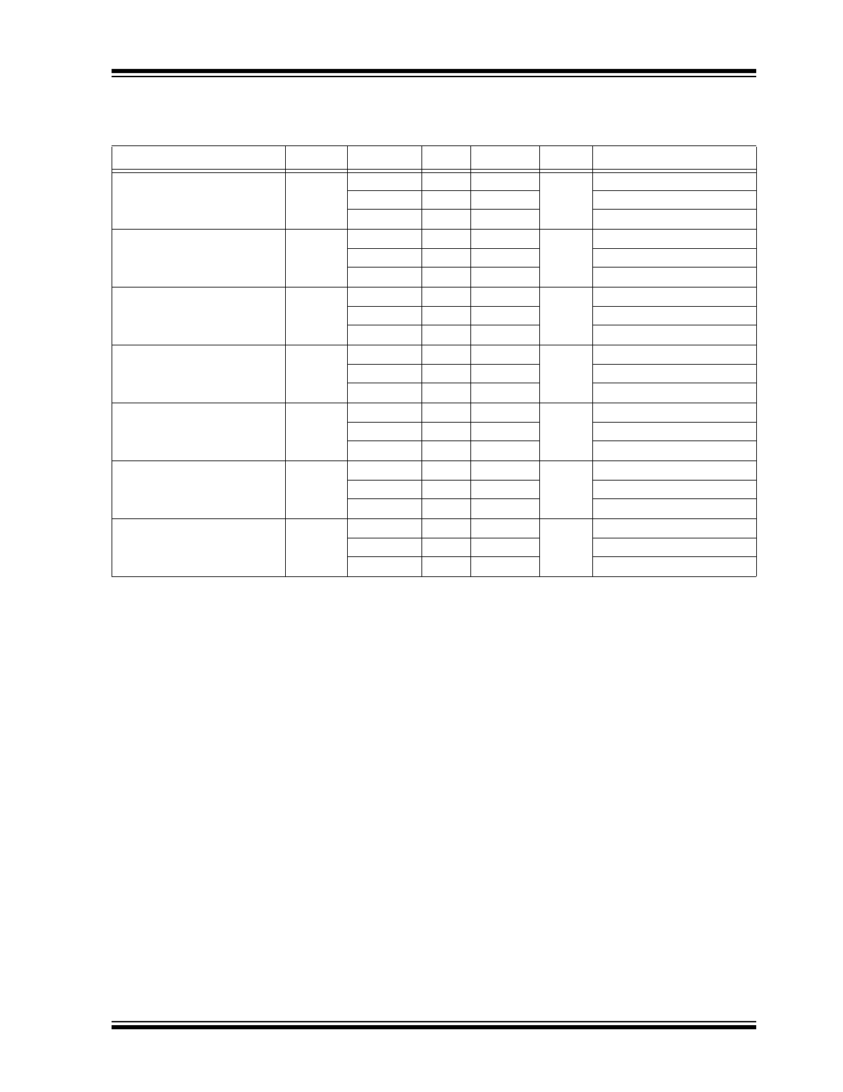
DC ELECTRICAL CHARACTERISTICS
Specifications: V
CC
= 2.5V; V
EE
= 0V. Input and output parameters vary 1:1 with V
CC
when V
CC
varies ±5%.
Parameters
Symbol
Min.
Typ.
Max.
Units
Conditions
Output High Voltage, (
Note 1
)
V
OH
1.415
1.520
1.620
V
At –40°C
1.475
1.550
1.620
At +25°C
1.475
1.550
1.620
At +85°C
Output Voltage Low, (
Note 1
)
V
OL
0.670
0.810
0.945
V
At –40°C
0.690
0.785
0.880
At +25°C
0.690
0.785
0.880
At +85°C
Input High Voltage
V
IH
1.275
—
1.620
V
At –40°C
1.335
—
1.620
At +25°C
1.335
—
1.620
At +85°C
Input Low Voltage
V
IL
0.670
—
1.090
V
At –40°C
0.690
—
1.025
At +25°C
0.690
—
1.025
At +85°C
Input High Voltage Common
Mode Range, (
Note 2
,
Note 3
)
V
CMR
1.2
—
2.5
V
At –40°C
1.2
—
2.5
At +25°C
1.2
—
2.5
At +85°C
Input High Current, (
Note 4
)
I
IH
—
—
60
µA
At –40°C
—
—
60
At +25°C
—
—
60
At +85°C
Input Low Current, (
Note 4
)
I
IL
–60
—
—
µA
At –40°C
–60
—
—
At +25°C
–60
—
—
At +85°C
Note 1: Outputs terminated with 50Ω to V
CCO
–2V.
2: Common mode voltage is defined as V
IH
.
3: For single-ended applications, the maximum input voltage for CLK-INx, CLK-INxB is V
CC
+0.3V.
4: CLK-IN0, CLK-IN1; CLK-IN0B, CLK-IN1B.
PL138-48
DS20005543B-page 4
2016 Microchip Technology Inc.
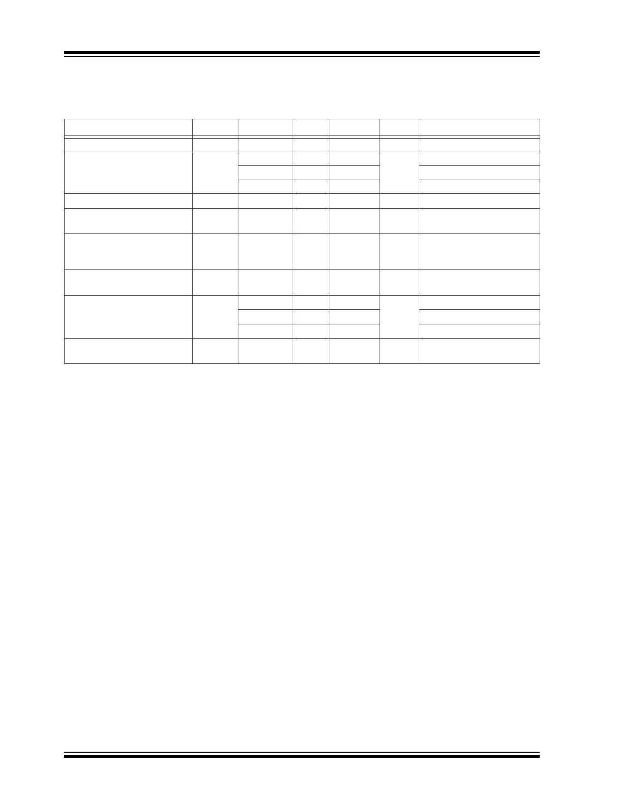
AC ELECTRICAL CHARACTERISTICS
V
CC
= –3.8V to –2.375 or V
CC
= 2.375V to 3.8V; V
EE
= 0V; T
A
= –40°C to +85°C. All parameters are measured at
f ≤ 800 MHz unless otherwise noted.
Parameters
Symbol
Min.
Typ.
Max.
Units
Conditions
Output Frequency
f
MAX
—
—
800
MHz
At all temperatures
Propagation Delay, (
Note 1
)
t
PD
600
680
750
ps
At –40°C
650
725
790
At +25°C
690
790
890
At +85°C
Output Skew, (
Note 2
,
Note 4
)
t
SK(O)
—
25
37
ps
At all temperatures
Part-to-Part Skew, (
Note 3
,
Note 4
)
t
SK(PP)
—
85
225
ps
At all temperatures
Buffer Additive Phase Jitter,
RMS
t
APJ
—
—
0.10
ps
At all temperatures; refer to
Noise Characteristics
section
Peak-to-Peak Input Voltage
(Differential Configuration)
V
PP
150
800
1200
mV
At all temperatures
Peak-to-Peak Output Voltage
V
SWING
470
800
950
mV
At –40°C
600
800
930
At +25°C
600
800
930
At +85°C
Output Rise/Fall Time
t
R
/t
F
200
—
550
ps
At all temperatures; 20% to
80% at full output swing.
Note 1: Measured from the differential input crossing point to the differential output crossing point.
2: Defined as skew between outputs at the same supply voltage and with equal load conditions. Measured at
the output differential cross points.
3: Defined as skew between outputs on different devices operating at the same supply voltages and with
equal load conditions. Using the same type of inputs on each device, the outputs are measured at the dif-
ferential cross points.
4: This parameter is defined in accordance with JEDEC Standard 65.
2016 Microchip Technology Inc.
DS20005543B-page 5
PL138-48
TEMPERATURE SPECIFICATIONS (
Note 1
)
Parameters
Sym.
Min.
Typ.
Max.
Units
Conditions
Temperature Ranges
Ambient Operating Temperature
T
A
–40
—
+85
°C
Note 2
Junction Temperature
T
J
—
—
+110
°C
—
Storage Temperature Range
T
S
–65
—
+150
°C
—
Soldering Temperature
—
—
—
+260
°C
10 sec.
Note 1: The maximum allowable power dissipation is a function of ambient temperature, the maximum allowable
junction temperature, and the thermal resistance from junction to air (i.e., T
A
, T
J
,
JA
). Exceeding the
maximum allowable power dissipation will cause the device operating junction temperature to exceed the
maximum +125°C rating. Sustained junction temperatures above +125°C can impact the device reliability.
2: Operating temperature is guaranteed by design for all parts (commercial and industrial), but tested for
commercial grade only.
PL138-48
DS20005543B-page 6
2016 Microchip Technology Inc.
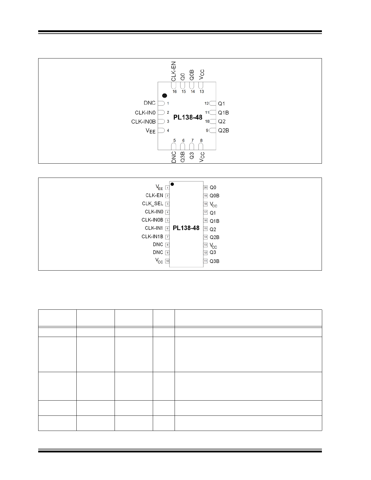
2.0
PIN DESCRIPTIONS
FIGURE 2-1:
Pin Configuration, 16-Pin QFN.
FIGURE 2-2:
Pin Configuration, 20-Pin TSSOP.
The descriptions of the pins are listed in
Table 2-1
.
TABLE 2-1:
PIN FUNCTION TABLE
Pin Number
QFN-16
Pin Number
TSSOP-20
Pin Name
Type
Description
4
1
V
EE
P
Power supply pin connection.
16
2
CLK-EN
I
Synchronizing clock enable.
When HIGH, clock outputs follow clock input. When LOW, Q
outputs are forced low, QB outputs are forced high.
LVTTL/LVCMOS interface levels.
50 kΩ internal pull-up resistor.
—
3
CLK-SEL
I
Clock select input. When HIGH, selects CLK1 input. When
LOW, selects CLK0 input.
LVTTL/LVCMOS interface levels.
50 kΩ internal pull-down resistor.
2
4
CLK-IN0
I
True part of differential clock input signal. 75 kΩ internal
pull-down resistor.
3
5
CLK-IN0B
I
Complementary part of differential clock input signal.
100 kΩ internal pull-up and pull-down resistors.
2016 Microchip Technology Inc.
DS20005543B-page 7
PL138-48
—
6
CLK-IN1
I
True part of differential clock input signal. 75 kΩ internal
pull-down resistor.
—
7
CLK-IN1B
I
Complementary part of differential clock input signal.
100 kΩ internal pull-up and pull-down resistors.
1, 5
8, 9
DNC
—
Do Not Connect.
8, 13
10, 13, 18
V
CC
P
Power supply pin connection.
6, 9, 11 ,14
11, 14, 16, 19
QB0 ~ QB3
O
LVPECL Complementary output.
7, 10, 12, 15
12, 15, 17, 20
Q0 ~ Q3
O
LVPECL True output.
TABLE 2-1:
PIN FUNCTION TABLE (CONTINUED)
Pin Number
QFN-16
Pin Number
TSSOP-20
Pin Name
Type
Description
PL138-48
DS20005543B-page 8
2016 Microchip Technology Inc.
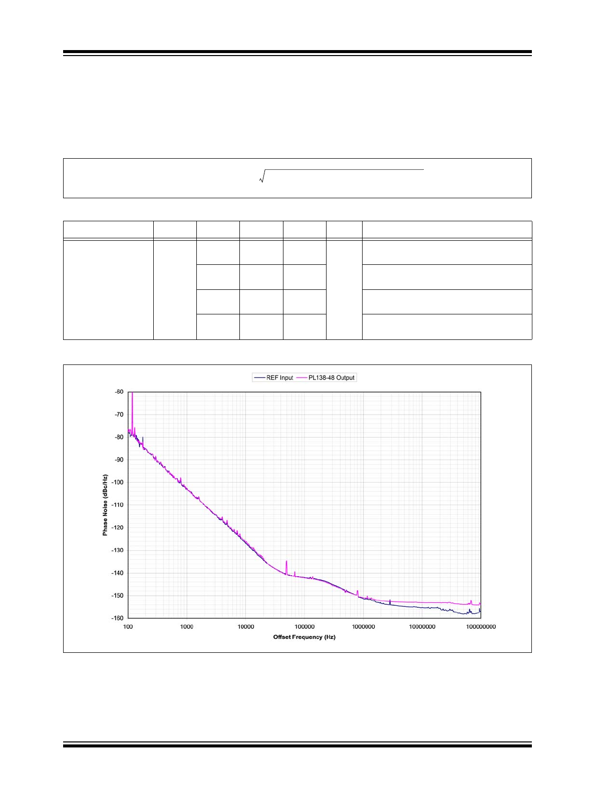
3.0
NOISE CHARACTERISTICS
When a buffer is used to pass a signal, the buffer adds a little bit of its own noise. The phase noise on the output of the
buffer will be a little bit more than the phase noise of the input signal. To quantify the noise addition in the buffer we
compare the Phase Jitter numbers from the input and the output. The difference is called "Additive Phase Jitter". The
formula for the Additive Phase Jitter is as follows:
EQUATION 3-1:
FIGURE 3-1:
PL138-48 Additive Phase Jitter Plot, 622 MHz.
TABLE 3-1:
PL138-48 NOISE CHARACTERISTICS
Parameters
Symbol
Min.
Typ.
Max.
Units Conditions
Additive Phase Jitter
t
APJ
—
20
40
fs
V
DD
= 3.3V, Frequency = 622.08 MHz
Offset = 12 kHz ~ 20 MHz
—
50
100
V
DD
= 3.3V, Frequency = 156.25 MHz
Offset = 12 kHz ~ 20 MHz
—
50
100
V
DD
= 3.3V, Frequency = 50 MHz
Offset = 1 kHz ~ 1 MHz
—
50
100
V
DD
= 3.3V, Frequency = 25 MHz
Offset = 1 kHz ~ 1 MHz
AdditivePhaseJitter
OutputPhaseJitter
2
InputPhaseJitter
2
–
=
2016 Microchip Technology Inc.
DS20005543B-page 9
PL138-48
4.0
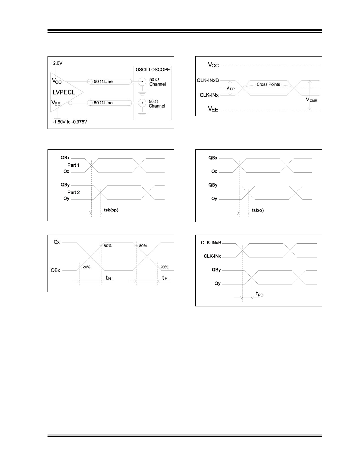
PARAMETER MEASUREMENT INFORMATION
FIGURE 4-1:
Output Waveform Test
Circuit.
FIGURE 4-2:
Part-to-Part Skew.
FIGURE 4-3:
Output Rise/Fall Time.
FIGURE 4-4:
Differential Input Level.
FIGURE 4-5:
Output Skew.
FIGURE 4-6:
Propagation Delay.
PL138-48
DS20005543B-page 10
2016 Microchip Technology Inc.
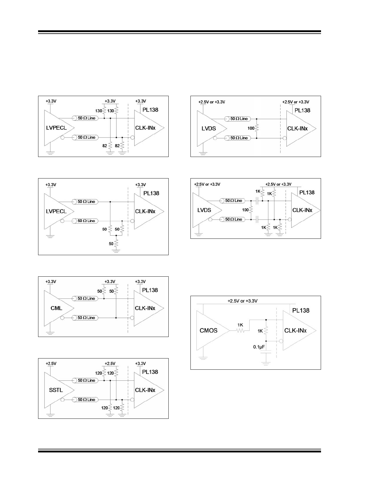
5.0
APPLICATION INFORMATION
5.1
Input Logic Configurations
The following circuits show different configurations for different input logic type signals. For good signal integrity at the
PL138 input, the signals need to be properly terminated according to the logic type requirements. The signals need to
be presented at the PL138 input according to V
CMR
, V
PP
, and other input requirements.
FIGURE 5-1:
CLK-IN Input Driven by a
3.3V LVPECL Driver.
FIGURE 5-2:
3.3V LVPECL Driver,
Alternative Termination.
FIGURE 5-3:
CLK-IN Input Driven by a
CML Driver.
FIGURE 5-4:
CLK-IN Input Driven by an
SSTL Driver.
FIGURE 5-5:
CLK-IN Input Driven by an
LVDS Driver.
FIGURE 5-6:
LVDS Driver, Alternative
AC-Coupling.
This circuit is for compatibility only. AC-coupling is not
really required for LVDS. The V
CMR
range of the PL138
reaches low enough that LVDS signals can be
connected directly to the PL138 input like in the circuit
in
Figure 5-5
.
FIGURE 5-7:
CLK-IN Input Driven by a
CMOS Driver.