
2018 Microchip Technology Inc.
DS20005835A-page 1
SY89297U
Features
• Dual-Channel, Programmable Delay Line
• Serial Programming Interface (SDATA, SCLK,
SLOAD)
• Guaranteed AC Performance over Temperature
and Voltage:
- >3.2 Gbps/1.6 GHz f
MAX
• Programming Accuracy:
- Linearity: –15 ps to +15 ps INL
- Monotonic: –5 ps to +25 ps
- Resolution: 5 ps Programming Increments
• Low-Jitter Design: 1 ps
RMS
Typical Random Jitter
• Programmable Delay Range: 5 ns Delay Range
• Cascade Capability for Increased Delay
• Flexible Voltage Operation:
- V
CC
= 2.5V ±5% or 3.3V ±10%
• Industrial Temperature Range: –40°C to +85°C
• Available in 24-Lead (4 mm x 4 mm) QFN
Package
Applications
• Clock De-Skewing
• Timing Adjustments
• Aperture Centering
• System Calibration
Markets
• Automated Test Equipment
• Digital Radio and Video Broadcasting
• Closed Caption Encoders/Decoders
• Test and Measurement
General Description
The SY89297U is a DC-3.2 Gbps programmable,
two-channel delay line. Each channel has a delay
range from 2 ns to 7 ns (5 ns delta delay) in
programmable increments as small as 5 ps. The delay
step is extremely linear and monotonic over the entire
programming range, with 15 ps INL over temperature
and voltage.
The delay varies in discrete steps based on a serial
control word provided by the 3-pin serial control
(SDATA, SCLK, and SLOAD). The control word for
each channel is 10-bits. Both channels are
programmed through a common serial interface. For
increased delay, multiple SY89297U delay lines can be
cascaded together.
The SY89297U provides two independent 3.2 Gbps
delay lines in an ultra-small 4 mm x 4 mm, 24-pin QFN
package. For other delay line solutions, consider the
SY89295U and SY89296U single-channel delay lines.
Evaluation boards are available for all these parts.
Package Type
SY89297U
24-Lead 4x4 QFN (M)
INA
/INA
VTA
VTB
INB
/INB
QA
/QA
VCC
VCC
QB
/QB
SOUT
S
D
ATA
SCLK
SLOAD
GND
VCC
/ENB
/ENA
GND
VREF-AC
GND
VCC
7
8
9
10
11
12
18
17
16
15
14
13
24
23
22
21
20
19
1
2
3
4
5
6
2.5V/3.3V, 3.2 Gbps, Precision CML
Dual-Channel Programmable Delay
United States Patent No. RE44,134
SY89297U
DS20005835A-page 2
2018 Microchip Technology Inc.
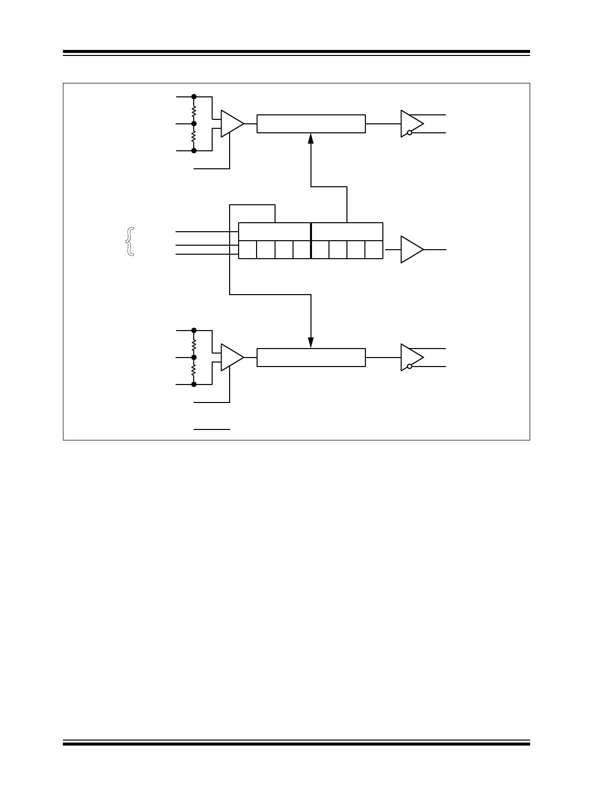
Functional Block Diagram
INA
VTA
/INA
/ENA
QA
/QA
CML
10 Bits
5ps/Step = 5ns
SLOAD
SDATA
SCLK
SOUT
TTL
Open-Collector
Resistor Pull-Up
LATCH B
LATCH A
D9B
...
D1B D0B D9A
...
D1A D0A
(TTL/CMOS)
INB
VTB
/INB
QB
/QB
CML
5ps/Step = 5ns
/ENB
VREF-AC
20 Bits
{
Serial
Interface
10 Bits
2018 Microchip Technology Inc.
DS20005835A-page 3
SY89297U
1.0
ELECTRICAL CHARACTERISTICS
Absolute Maximum Ratings †
Supply Voltage (V
CC
) ................................................................................................................................ –0.5V to +4.0V
Input Voltage (V
IN
) ....................................................................................................................................... –0.5V to V
CC
CML Output Voltage (V
OUT
) ..................................................................................................... V
CC
– 1.0V to V
CC
+ 0.5V
Current (Source or Sink Current on V
T
) ................................................................................................................±70 mA
Input Current (Source or Sink Current on IN, /IN) .................................................................................................±35 mA
Current (V
REF
, Source or Sink Current on V
REF-AC
) (
Note 1
)..............................................................................±0.5 mA
Operating Ratings ‡
Supply Voltage (V
CC
for T
A
= –40°C to +85°C)................................................................................. +2.375V to +2.625V
Supply Voltage (V
CC
for T
A
= –40°C to +75°C)......................................................................................... +3.0V to +3.6V
†
Notice: Stresses above those listed under “Absolute Maximum Ratings” may cause permanent damage to the device.
This is a stress rating only and functional operation of the device at those or any other conditions above those indicated
in the operational sections of this specification is not intended. Exposure to maximum rating conditions for extended
periods may affect device reliability.
‡ Notice:
The device is not guaranteed to function outside its operating ratings.
Note 1:
Due to the limited drive capability, use for input of the same package only.
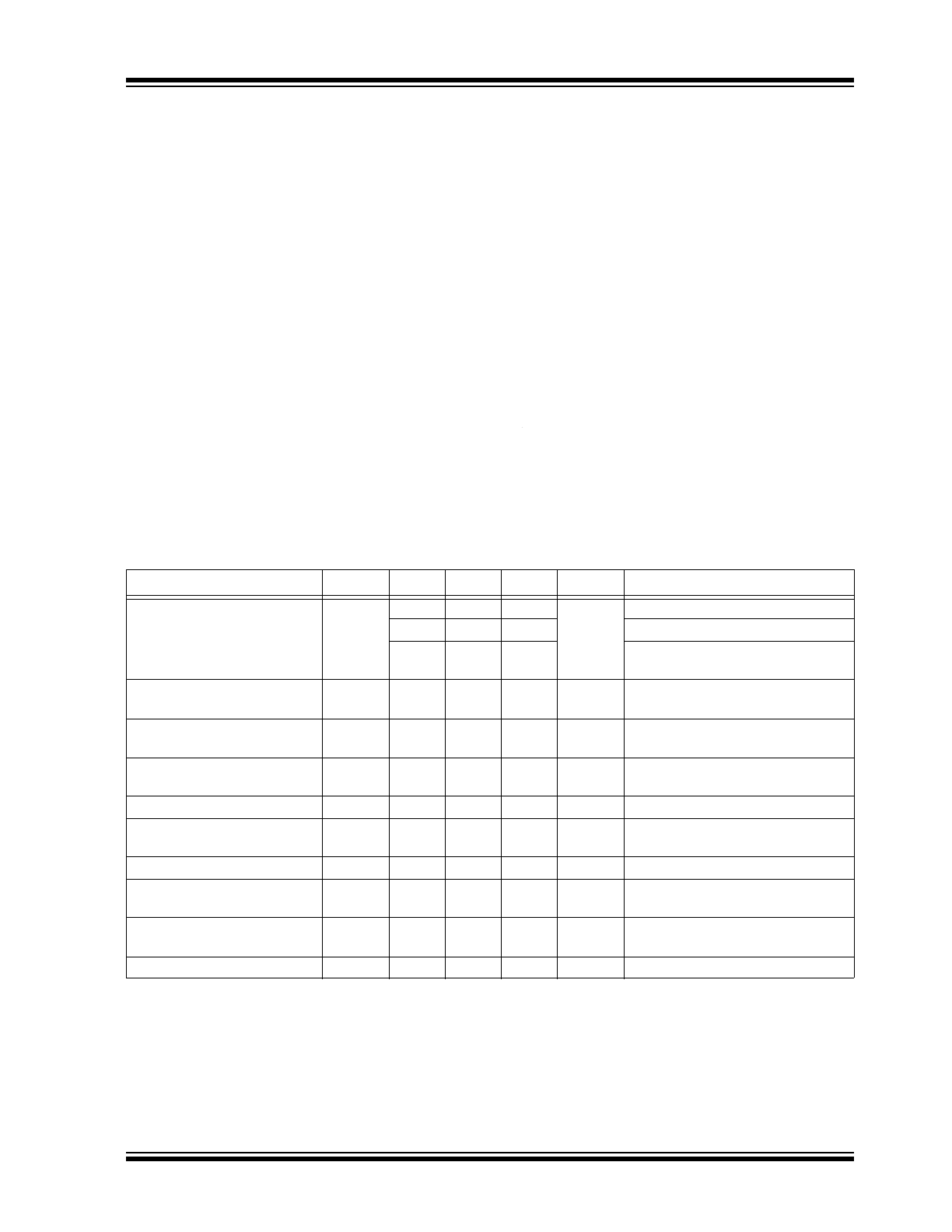
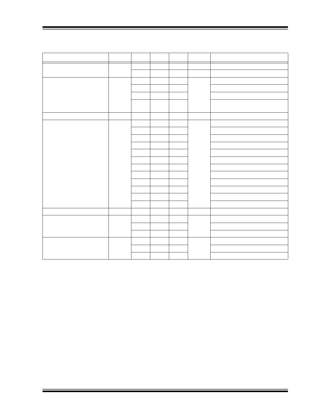
TABLE 1-1:
DC ELECTRICAL CHARACTERISTICS
Electrical Characteristics:
T
A
= –40°C to +85°C, Channels A and B, unless noted.
Note 1
Parameter
Symbol
Min.
Typ.
Max.
Units
Conditions
Power Supply Voltage Range
V
CC
2.375
2.5
2.625
V
T
A
= –40°C to +85°C
3.0
3.3
3.6
T
A
= –40°C to +75°C
3.0
3.3
3.6
T
A
= –40°C to +85°C, Airflow =
500 lfpm
Power Supply Current
I
CC
—
195
250
mA
Maximum V
CC
, Both Channels
Combined, Output Load Included
Input Resistance
(IN-to-VT, /IN-to-VT)
R
IN
45
50
55
Ω
—
Differential Input Resistance
(IN-to-/IN)
R
DIFF_IN
90
100
110
Ω
—
Input HIGH Voltage (IN, /IN)
V
IH
1.2
—
V
CC
V
—
Input LOW Voltage (IN, /IN)
V
IL
0
—
V
IH
–
0.1
V
—
Input Voltage Swing (IN, /IN)
V
IN
0.1
—
1.0
V
See
Figure 5-1
Differential Input Voltage
Swing (|IN - /IN|)
V
DIFF_IN
0.2
—
—
V
See
Figure 5-2
Output Reference Voltage
V
REF-AC
V
CC
–
1.3
V
CC
–
1.2
V
CC
–
1.1
V
—
Voltage from Input to V
T
V
T_IN
—
—
1.28
V
—
Note 1:
The circuit is designed to meet the DC specifications show in the table above after thermal equilibrium has
been established.
SY89297U
DS20005835A-page 4
2018 Microchip Technology Inc.
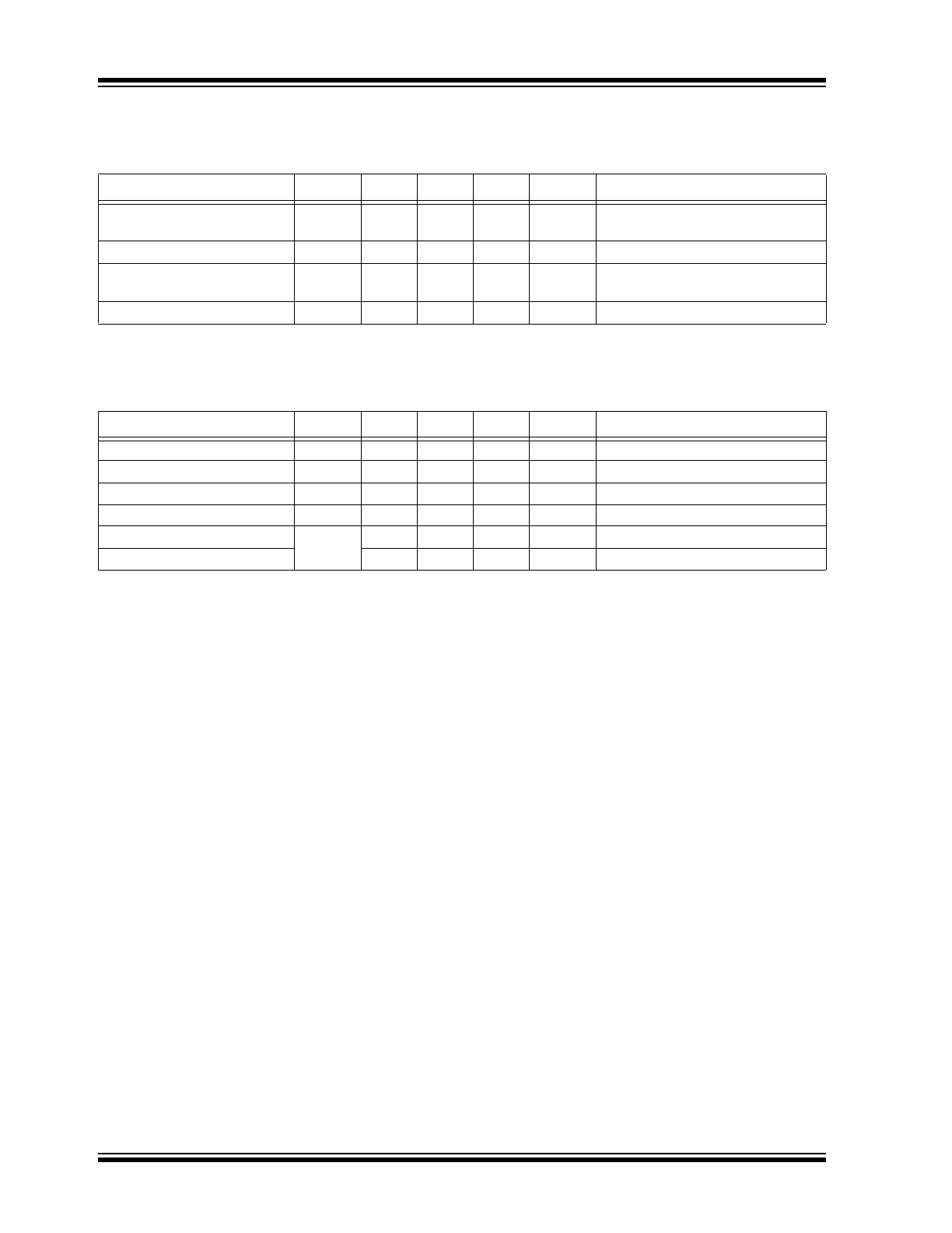
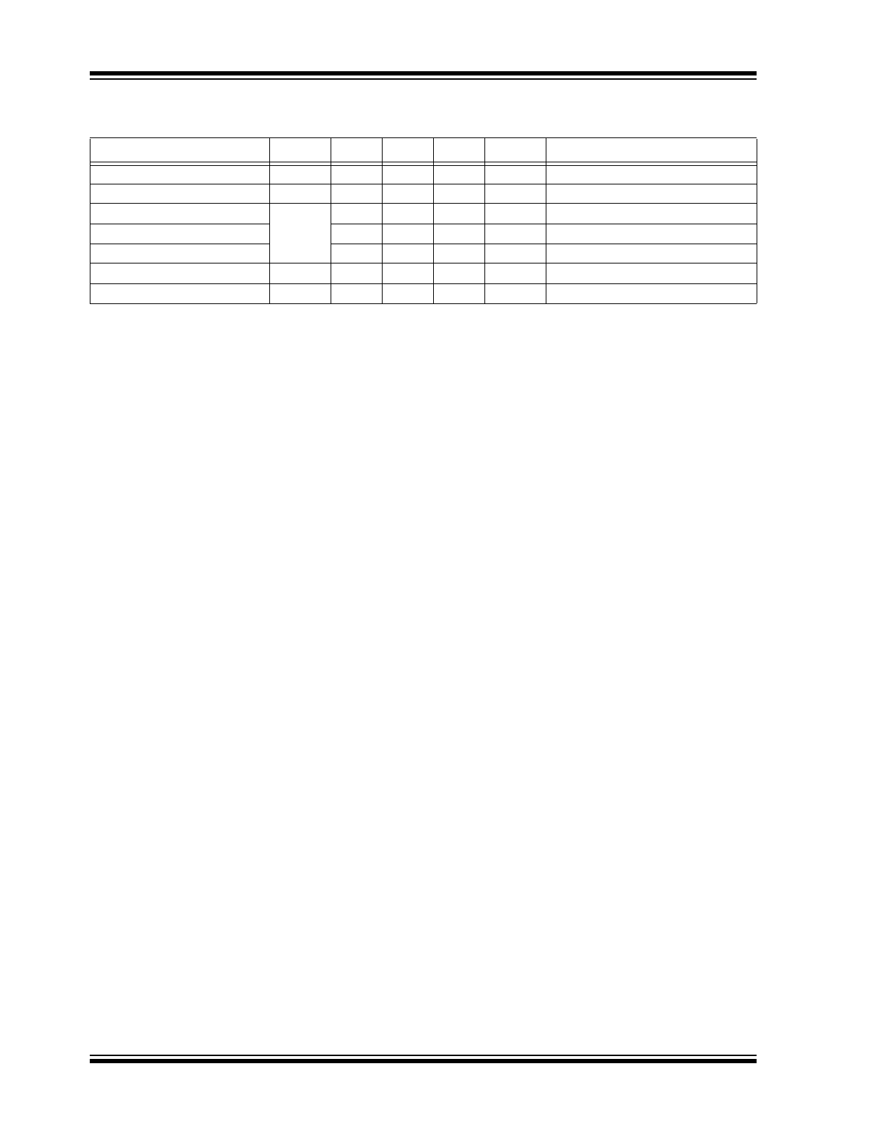
TABLE 1-2:
CML OUTPUTS DC ELECTRICAL CHARACTERISTICS
Electrical Characteristics:
V
CC
= +2.5V +5% or +3.3V ±10%, R
L
= 100Ω across the outputs; T
A
= –40°C to +85°C,
unless otherwise stated.
Note 1
Parameter
Symbol
Min.
Typ.
Max.
Units
Conditions
Output HIGH Voltage
V
OH
V
CC
–
0.02
V
CC
–
0.01
V
CC
V
R
L
= 50Ω to V
CC
Output Voltage Swing
V
OUT
325
400
—
mV
See
Figure 5-1
Differential Output Voltage
Swing
V
DIFF_OUT
650
800
—
mV
See
Figure 5-2
Output Source Impedance
R
OUT
45
50
55
Ω
—
Note 1:
The circuit is designed to meet the DC specifications shown in the above table after thermal equilibrium
has been established.
TABLE 1-3:
LVTTL/CMOS DC ELECTRICAL CHARACTERISTICS
Electrical Characteristics:
V
CC
= 2.5V ±5% or 3.3V ±10%; T
A
= –40°C to +85°C; unless otherwise stated.
Note 1
Parameter
Symbol
Min.
Typ.
Max.
Units
Conditions
Input High Voltage
V
IH
2.0
—
—
V
—
Input Low Voltage
V
IL
—
—
0.8
V
—
Input High Current
I
IH
—
—
150
µA
V
IH
= V
CC
Input Low Current
I
IL
—
—
50
µA
V
IL
= 0.8V
Output LOW Voltage
V
OL
—
—
0.55
V
SOUT Pin; I
OL
= 1 mA
Output High Leakage Current
—
—
100
µA
SOUT = V
CC
Note 1:
The circuit is designed to meet the DC specifications shown in the above table after thermal equilibrium
has been established.
2018 Microchip Technology Inc.
DS20005835A-page 5
SY89297U
TABLE 1-4:
AC ELECTRICAL CHARACTERISTICS
Electrical Characteristics:
T
A
= –40°C to +85°C, Channels A and B, unless otherwise stated.
Note 1
Parameter
Symbol
Min.
Typ.
Max.
Units
Conditions
Maximum Operating
Frequency
f
MAX
1.6
—
—
GHz
Clock: V
OUT
Swing >200 mV
pk
3.2
—
—
Gbps
NRZ Data
Propagation Delay
t
pd
1000
—
2000
ps
IN to Q; D[0-9] = 0
5500
—
7500
IN to Q; D[0-9] = 1023
1000
—
2500
/EN to Q: D[0-9] = 0; V
TH
= V
CC
/2
2000
—
4500
SDATA to SOUT (D0-D9 = Low),
No load
Programmable Range
t
RANGE
4150
5115
—
ps
t
pd(MAX)
– t
pd(MIN)
Step Delay
∆t
—
5
—
ps
D0 High
—
10
—
D1 High
—
20
—
D2 High
—
40
—
D3 High
—
80
—
D4 High
—
160
—
D5 High
—
320
—
D6 High
—
640
—
D7 High
—
1280
—
D8 High
—
2560
—
D9 High
—
5115
—
D0-D9 High
–5
—
25
Monotonic
Integral Non-Linearity
INL
–15
—
15
ps
Note 2
Set-Up Time
t
S
400
—
—
ps
SDATA to SCLK
400
—
—
SCLK to SLOAD,
Note 3
300
—
—
/EN to IN,
Note 4
Hold Time
t
H
300
—
—
ps
SLOAD to SCLK,
Note 5
–100
—
—
IN to /EN,
Note 6
200
—
—
SCLK to SDATA
SY89297U
DS20005835A-page 6
2018 Microchip Technology Inc.
Pulse Width
t
PW
1000
—
—
ps
SLOAD
Release Time
t
R
800
—
—
ps
/EN to IN,
Note 7
Cycle-to-Cycle Jitter
t
JITTER
—
—
2
ps
RMS
Note 8
Total Jitter
—
—
20
ps
PP
Note 9
Random Jitter
—
—
2
ps
RMS
Note 10
Output Rise/Fall Time
t
r
/t
f
30
55
80
ps
20% to 80% (Q)
Duty Cycle
—
45
—
55
%
Input frequency = 1.6 GHz
Note 1:
High frequency AC electricals are guaranteed by design and characterization.
2:
INL (Integral Non-Linearity) is defined from its corresponding point on the ideal delay versus D[9:0] curve
as the deviation from its ideal delay. The maximum difference is the INL. Theoretical Ideal Linearity (TIL) =
(measured maximum delay – measured minimum delay) ÷ 1023. INL = measured delay – (measured min-
imum delay + (step number x TIL)).
3:
SCLK has to transition L-H a setup time before the SLOAD H-L transition to ensure the valid data is prop-
erly latched. See
Figure 4-2
.
4:
This setup time is the minimum time that /EN must be asserted prior to the next transition of IN / /IN to pre-
vent an output response greater than ±75 mV to that IN or /IN transition. See
Figure 4-3
.
5:
SCLK has to transition L-H a hold time after the SLOAD H-L transition to ensure that the valid data is prop-
erly latched before starting to load new data. See
Figure 4-2
.
6:
This hold time is the minimum time that /EN must remain asserted after a negative going transition of IN to
prevent an output response greater than ±75 mV to the IN transition. See
Figure 4-3
.
7:
This release time is the minimum time that /EN must be de-asserted prior to the next IN / /IN transition to
affect the propagation delay of IN to Q less than 1 ps. See
Figure 4-3
.
8:
Cycle-to-cycle jitter definition: The variation of periods between adjacent cycles over a random sample of
adjacent cycle pairs T
jitter_cc
= T
n
– T
n
+1, where T is the time between rising edges of the output signal.
9:
Total jitter definition: With an ideal clock input, no more than one output edge in 10
12
output edges will
deviate by more than the specified peak-to-peak jitter value.
10:
Random jitter definition: Jitter that is characterized by a Gaussian distribution, unbounded and is quanti-
fied by its standard deviation and mean. Random jitter is measured with a K28.7 comma detect pattern,
measured at 1.5 Gbps.
TABLE 1-4:
AC ELECTRICAL CHARACTERISTICS (CONTINUED)
Electrical Characteristics:
T
A
= –40°C to +85°C, Channels A and B, unless otherwise stated.
Note 1
Parameter
Symbol
Min.
Typ.
Max.
Units
Conditions
2018 Microchip Technology Inc.
DS20005835A-page 7
SY89297U
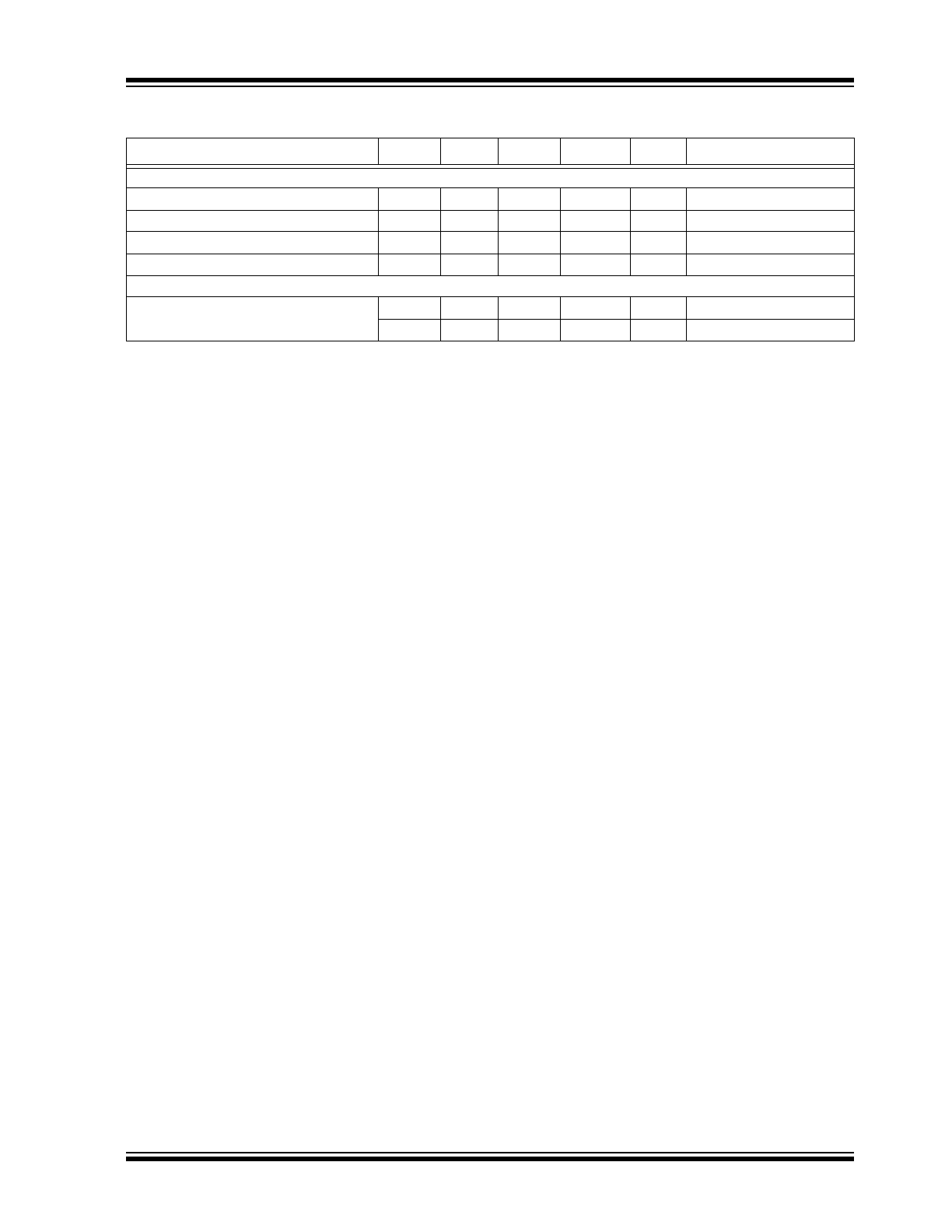
TEMPERATURE SPECIFICATIONS (
Note 1
)
Parameters
Sym.
Min.
Typ.
Max.
Units
Conditions
Temperature Ranges
Junction Operating Temperature
T
J
—
—
+125
°C
—
Storage Temperature Range
T
S
–65
—
+150
°C
—
Lead Temperature
—
—
—
+260
°C
Soldering, 20s
Ambient Temperature Range
T
A
–40
—
+85
°C
—
Package Thermal Resistances,
Note 2
Thermal Resistance QFN-24
JA
—
43
—
°C/W
Still-Air
Ψ
JB
—
30.5
—
°C/W
Junction-to-Board
Note 1:
The maximum allowable power dissipation is a function of ambient temperature, the maximum allowable
junction temperature and the thermal resistance from junction to air (i.e., T
A
, T
J
,
JA
). Exceeding the
maximum allowable power dissipation will cause the device operating junction temperature to exceed the
maximum +125°C rating. Sustained junction temperatures above +125°C can impact the device reliability.
2:
Thermal performance on QFN packages assumes exposed pad is soldered (or equivalent) to the device
most negative potential (GND).
SY89297U
DS20005835A-page 8
2018 Microchip Technology Inc.
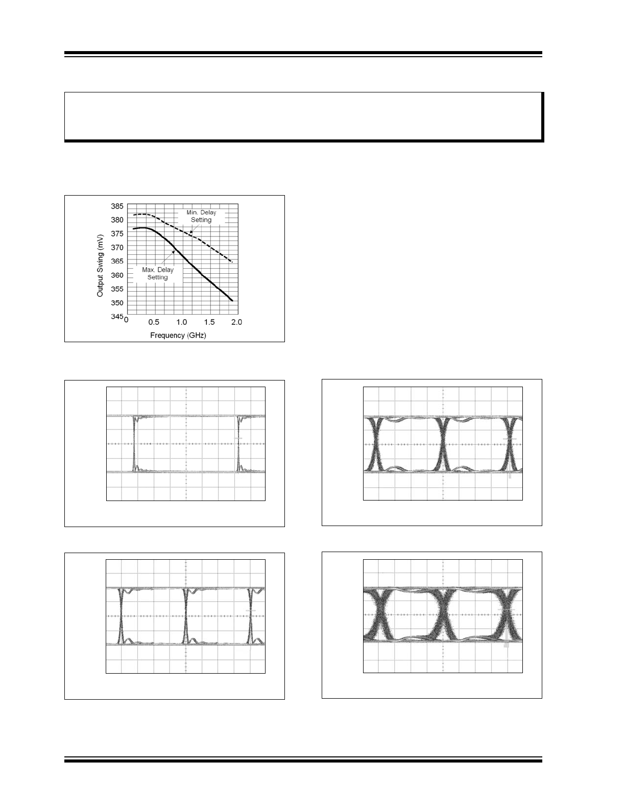
2.0
TYPICAL PERFORMANCE CURVES
V
CC
= +2.5V, GND = 0V, V
IN
= 100 mV, R
L
= 100Ω across the outputs, T
A
= +25°C for
Figure 2-1
.
V
CC
= 2.5V or 3.3V, GND = 0V, V
IN
= 100 mV, R
L
= 100Ω across the outputs, T
A
= +25°C, Maximum Delay (D0-D9 =
High) for
Figure 2-2
through
Figure 2-5
.
FIGURE 2-1:
Output Swing vs.
Frequency.
FIGURE 2-2:
155 Mbps Clock.
FIGURE 2-3:
622 Mbps Clock.
FIGURE 2-4:
1.6 Gbps Clock.
FIGURE 2-5:
3.2 Gbps Clock.
Note:
The graphs and tables provided following this note are a statistical summary based on a limited number of
samples and are provided for informational purposes only. The performance characteristics listed herein
are not tested or guaranteed. In some graphs or tables, the data presented may be outside the specified
operating range (e.g., outside specified power supply range) and therefore outside the warranted range.
Time (1ns/div.)
Output Swing
(100mV/div
.)
Time (400ps/div.)
Output Swing
(100mV/div
.)
Time (150ps/div.)
Output Swing
(100mV/div
.)
Time (80ps/div.)
Output Swing
(100mV/div
.)
2018 Microchip Technology Inc.
DS20005835A-page 9
SY89297U
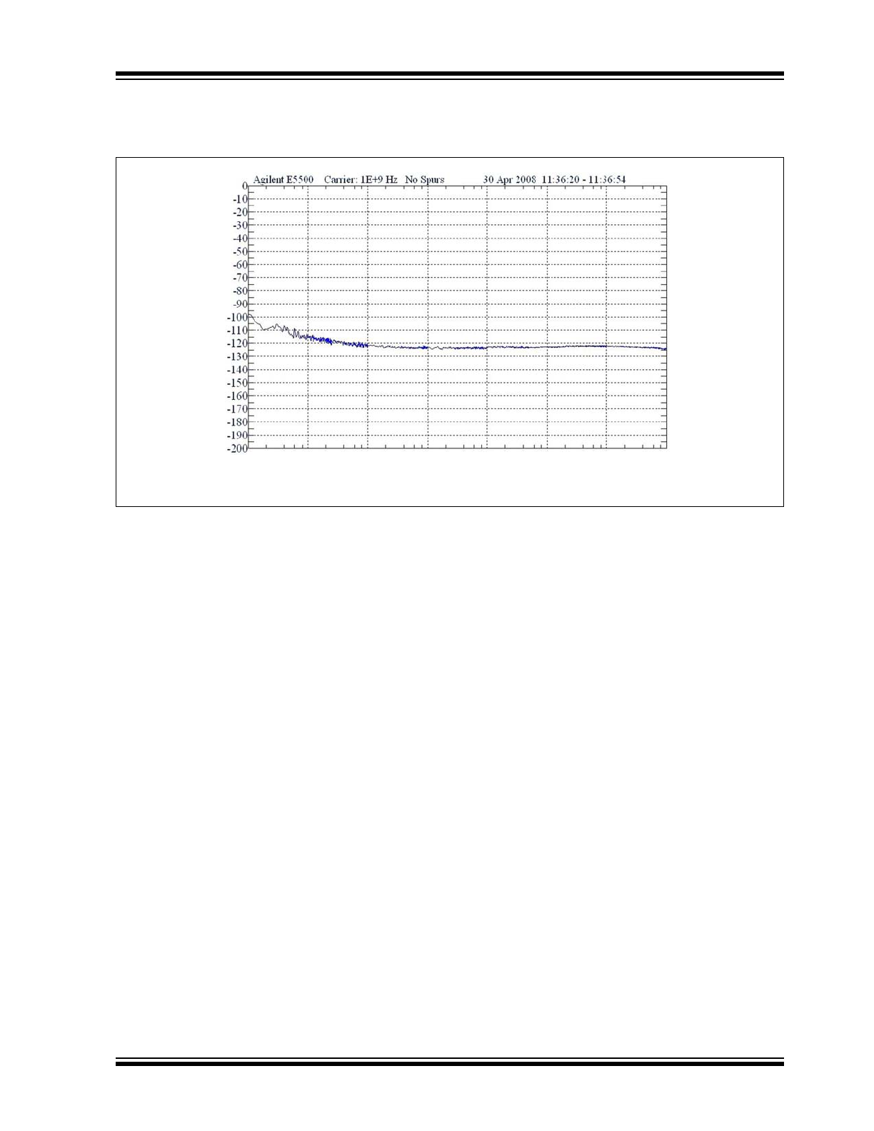
2.1
Phase Noise Chart
V
CC
= +2.5V, GND = 0V, V
IN
= 100 mV, R
L
= 100Ω across the outputs, T
A
= +25°C.
FIGURE 2-6:
f
C
: 1 GHz. Delay Setting: 00001 00110 (2 ns).
L(f) [dBc/Hz] vs. f[Hz]
10
100
1K
10K
100K
1M
10M
100M
SY89297U
DS20005835A-page 10
2018 Microchip Technology Inc.
3.0
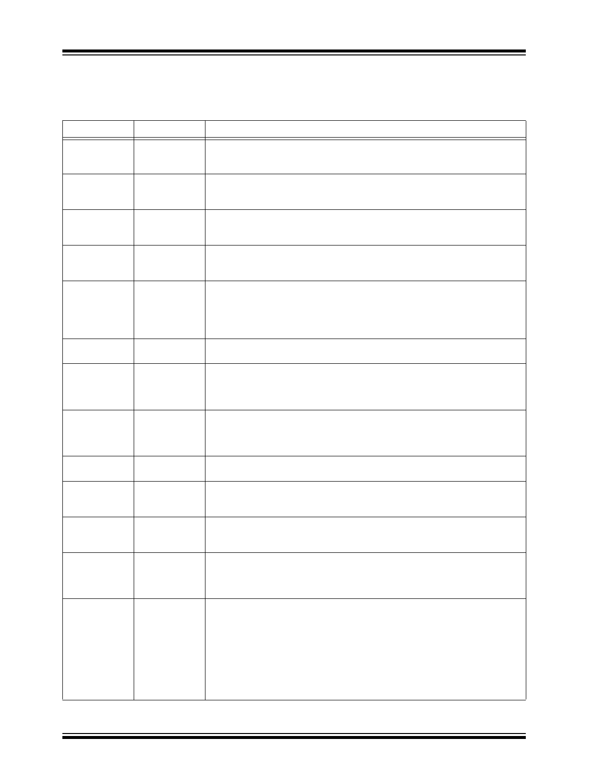
PIN DESCRIPTIONS
The descriptions of the pins are listed in
Table 3-1
.
TABLE 3-1:
PIN FUNCTION TABLE
Pin Number
Pin Name
Description
1, 2
INA, /INA
Channel A Differential Input: INA and /INA pins receive the Channel A data. QA
and /QA are the delayed product of INA and /INA. Each input is internally
terminated to VTA through a 50Ω resistor (100Ω across INA and /INA).
3
VTA
Input A Termination Center-Tap: Each side of the differential input pair
terminates to this pin. This pin provides a center-tap to a termination network for
maximum interface flexibility. See the
Input Interface Applications
section.
4
VTB
Input B Termination Center-Tap: Each side of the differential input pair
terminates to this pin. This pin provides a center-tap to a termination network for
maximum interface flexibility. See the
Input Interface Applications
section.
5, 6
INB, /INB
Channel B Differential Input: INB and /INB pins receive the Channel B data. QB
and /QB are the delayed product of INB and /INB. Each input is internally
terminated to VTB through a 50Ω resistor (100Ω across INB and /INB).
7
VREF-AC
Reference Voltage Output: For AC-coupled input signals, this pin can bias the
inputs IN and /IN. Connect VREF-AC directly to the VT input pin for each
channel. De-couple to V
CC
using a 0.01 µF capacitor. Maximum sink/source
current is ±0.5 mA. For DC-coupled input applications, leave VREF-AC pin
floating.
8, 11, 20
GND,
Exposed Pad
Negative Supply: Exposed pad must be connected to a ground plane that is the
same potential as the ground pins.
9
/ENA
CMOS/TTL-Compatible Enable Input: When the /ENA pin is pulled HIGH, QA is
held LOW and /QA goes HIGH after the programmed delay propagates through
the part. /ENA contains a 67 kΩ pull-down resistor and defaults LOW when left
floating. Logic threshold level is V
CC
/2
10
/ENB
CMOS/TTL-Compatible Enable Input: When the /ENB pin is pulled HIGH, QB is
held LOW and /QB goes HIGH after the programmed delay propagates through
the part. /ENB contains a 67 kΩ pull-down resistor and defaults LOW when left
floating. Logic threshold level is V
CC
/2
12, 15, 16, 19
VCC
Power Supply: Bypass each supply pin with 0.1 µF//0.01 µF low-ESR
capacitors. See
Table 1-1
for more details. 2.5V ±5% or 3.3V ±10%.
13, 14
/QB, QB
CML Differential Output: QB and /QB are the delayed product of INB, /INB. CML
outputs are terminated at the destination with 100Ω across the pair. See the
CML Output Termination
section.
17, 18
/QA, QA
CML Differential Output: QA and /QA are the delayed product of INA, /INA. CML
outputs are terminated at the destination with 100Ω across the pair. See the
CML Output Termination
section.
21
SOUT
CMOS/TTL-compatible output: This pin is used to support cascading multiple
SY89297U delay lines. Serial data is clocked into the SDATA input and is
clocked out of SOUT into the next SY89297U delay line. SOUT pin includes an
internal 550Ω pull-up resistor.
22, 23
SDATA, SCLK
CMOS/TTL-compatible 3-pin serial programming control inputs: The 3-pin serial
control sets each channel’s IN to Q delay. DA(0:9) control channel A delay.
DB(0:9) control channel B. To program the two channels, insert a 20-bit word
(DA0:DA9 and DB0:DB9) into SDATA and clock in the control bits with SCLK.
Maximum input frequency to SCLK is 40 MHz. Data is loaded into the serial
registers on the L-H transition of SCLK. After all 20-bits are clocked in, SLOAD
latches the new delay bits. These pins have internal pull-downs at the inputs.
See
Table 1-4
for delay values. Logic threshold level is V
CC
/2. SCLK and SDATA
contain a 67 kΩ pull-down resistor and default LOW when left floating.