

© 2011 Microchip Technology Inc.
DS25006A-page 1
MCP14E6/7/8
Features
• High Peak Output Current: 2.0A (typical)
• Independent Enable Function for Each Driver
Output
• Wide Input Supply Voltage Operating Range:
- 4.5V to 18V
• Low Shoot-Through/Cross-Conduction Current in
Output Stage
• High Capacitive Load Drive Capability:
- t
R
: 12 ns with 1000 pF load (typical)
- t
F
: 15 ns with 1000 pF load (typical)
• Short Delay Times: 45 ns (typical)
• Low Supply Current:
- With Logic ‘1’ Input/Enable – 1 mA (typical)
- With Logic ‘0’ Input/Enable – 300 µA (typical)
• Latch-up Protected: Passed JEDEC JESD78A
• Logic Input will Withstand Negative Swing,
up to 5V
• Space-Saving Packages:
- 8-Lead SOIC, PDIP, 6x5 DFN
Applications
• Switch Mode Power Supplies
• Pulse Transformer Drive
• Line Drivers
• Motor and Solenoid Drive
General Description
The MCP14E6/7/8 devices are high-speed MOSFET
drivers, capable of providing 2.0A of peak current. The
dual inverting, dual non-inverting and complementary
outputs are directly controlled from either TTL or
CMOS (3V to 18V). These devices also feature low
shoot-through current, fast rise/fall times and
propagation delays, which make them ideal for high
switching frequency applications.
The MCP14E6/7/8 devices operate from a 4.5V to 18V
single power supply and can easily charge and
discharge 1000 pF of MOSFET gate capacitance. They
provide low enough impedances, in both the ON and
OFF states, to ensure the MOSFETs’ intended state
will not be affected, even by large transients.
The additional control of the MCP14E6/7/8 outputs is
allowed by the use of separate enable functions. The
ENB_A and ENB_B pins are active-high and are
internally pulled up to V
DD
. The pins may be left floating
for standard operation.
The MCP14E6/7/8 dual output, 2.0A driver family is
offered in both surface-mount and pin-through-hole
packages with a -40
o
C to +125
o
C temperature rating.
The low thermal resistance of the thermally enhanced
DFN package allows greater power dissipation
capability for driving heavier capacitive or resistive
loads.
These devices are highly latch-up resistant under any
conditions within their power and voltage ratings. They
are not subject to damage when up to 5V of noise
spiking (of either polarity) occurs on the ground pin.
The devices are fully latch-up protected when tested
according to JEDEC JESD78A. All terminals are fully
protected against Electrostatic Discharge (ESD), up to
4 kV (HBM) or 400V (MM).
2.0A Dual High-Speed Power MOSFET Driver With Enable
MCP14E6/7/8
DS25006A-page 2
© 2011 Microchip Technology Inc.
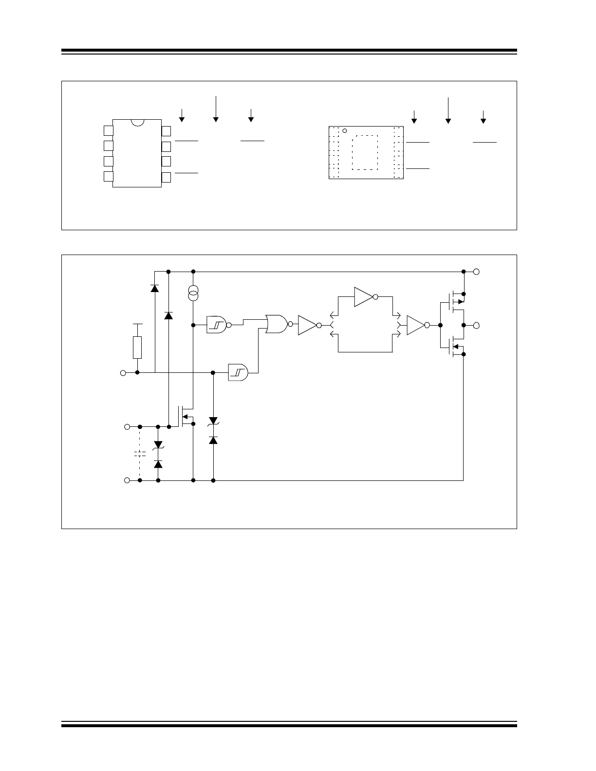
Package Types
Functional Block Diagram
(1)
ENB_A
GND
IN A
IN B
V
DD
OUT B
OUT A
ENB_B
V
DD
OUT B
OUT A
ENB_B
V
DD
OUT B
OUT A
ENB_B
6x5 DFN*
1
2
3
4
8
7
6
5
* Includes Exposed Thermal Pad (EP); see
Table 3-1
.
EP
9
1
2
3
4
5
6
7
8
ENB_A
GND
IN A
V
DD
OUT B
IN B
OUT A
ENB_B
V
DD
OUT B
OUT A
ENB_B
V
DD
OUT B
OUT A
ENB_B
PDIP, SOIC
MCP14E6
MCP14E8
MCP14E7
MCP14E6
MCP14E8
MCP14E7
Effective
Input C = 20 pF
(Each Input)
Output
Input
GND
V
DD
4.7 V
Inverting
Non-Inverting
Note 1:
Unused inputs should be grounded.
Enable
V
DD
Internal
Pull-up
4.7 V
MCP14E6 Dual Inverting
MCP14E7 Dual Non-Inverting
MCP14E8 One Inverting, One Non-Inverting
© 2011 Microchip Technology Inc.
DS25006A-page 3
MCP14E6/7/8
1.0
ELECTRICAL
CHARACTERISTICS
Absolute Maximum Ratings †
Supply Voltage ................................................................+20V
Input Voltage ............................... (V
DD
+ 0.3V) to (GND – 5V)
Enable Voltage .............................(V
DD
+ 0.3V) to (GND - 5V)
Input Current (V
IN
>V
DD
)................................................50 mA
Package Power Dissipation (T
A
= +50
o
C)
8L-DFN ........................................................................
Note 3
8L-PDIP ........................................................................1.12W
8L-SOIC .....................................................................669 mW
† Notice:
Stresses above those listed under "Maximum
Ratings" may cause permanent damage to the device.
This is a stress rating only and functional operation of
the device at those or any other conditions above those
indicated in the operational sections of this specifica-
tion is not intended. Exposure to maximum rating
conditions for extended periods may affect device
reliability.
DC CHARACTERISTICS
(2)
Electrical Specifications:
Unless otherwise indicated, T
A
= +25°C, with 4.5V
≤ V
DD
≤ 18V.
Parameters
Sym
Min
Typ
Max
Units
Conditions
Input
Logic ‘1’, High Input Voltage
V
IH
2.4
1.5
—
V
Logic ‘0’, Low Input Voltage
V
IL
—
1.3
0.8
V
Input Current
I
IN
-1
—
1
µA
0V
≤ V
IN
≤ V
DD
Input Voltage
V
IN
-5
—
V
DD
+ 0.3
V
Output
High Output Voltage
V
OH
V
DD
– 0.025
—
—
V
DC Test
Low Output Voltage
V
OL
—
—
0.025
V
DC Test
Output Resistance, High
R
OH
—
5
8
Ω
I
OUT
= 10 mA, V
DD
= 18V
Output Resistance, Low
R
OL
—
5
8
Ω
I
OUT
= 10 mA, V
DD
= 18V
Peak Output Current
I
PK
—
2
—
A
V
DD
= 18V
(2)
Switching Time
(1)
Rise Time
t
R
—
12
30
ns
Figure 4-1
,
Figure 4-2
,
C
L
= 1000 pF
Fall Time
t
F
—
15
35
ns
Figure 4-1
,
Figure 4-2
,
C
L
= 1000 pF
Propagation Delay Time
t
D1
—
45
55
ns
Figure 4-1
,
Figure 4-2
Propagation Delay Time
t
D2
—
45
55
ns
Figure 4-1
,
Figure 4-2
Enable Function (ENB_A, ENB_B)
High-Level Input Voltage
V
EN_H
2.4
1.6
—
V
V
DD
= 12V, Low-to-High Transition
Low-Level Input Voltage
V
EN_L
—
1.2
0.8
V
V
DD
= 12V, High-to-Low Transition
Hysteresis
V
HYST
—
400
—
mV
Enable Pull-up Impedance
R
ENBL
0.7
1.6
3.0
M
Ω
V
DD
= 14V, ENBL = GND
Enable Pin Leakage Current
I
ENBL
—
10
—
µA
V
DD
= 12V,
ENB_A = ENB_B = GND
Propagation Delay Time
t
D3
—
35
65
ns
V
DD
= 12V,
Figure 4-3
Propagation Delay Time
t
D4
—
35
65
ns
V
DD
= 12V,
Figure 4-3
Note 1:
Switching times are ensured by design.
2:
Tested during characterization, not production tested.
3:
Package power dissipation is dependent on the copper pad area of the PCB.
MCP14E6/7/8
DS25006A-page 4
© 2011 Microchip Technology Inc.
Power Supply
Supply Voltage
V
DD
4.5
—
18.0
V
Supply Current
I
DD
—
1000
1800
µA
V
IN_A
= 3V, V
IN_B
= 3V,
ENB_A = ENB_B = High
I
DD
—
600
900
µA
V
IN_A
= 0V, V
IN_B
= 0V,
ENB_A = ENB_B = High
I
DD
—
800
1600
µA
V
IN_A
= 3V, V
IN_B
= 0V,
ENB_A = ENB_B = High
I
DD
—
800
1600
µA
V
IN_A
= 0V, V
IN_B
= 3V,
ENB_A = ENB_B = High
I
DD
—
600
1000
µA
V
IN_A
= 3V, V
IN_B
= 3V,
ENB_A = ENB_B = Low
I
DD
—
300
450
µA
V
IN_A
= 0V, V
IN_B
= 0V,
ENB_A = ENB_B = Low
I
DD
—
500
800
µA
V
IN_A
= 3V, V
IN_B
= 0V,
ENB_A = ENB_B = Low
I
DD
—
500
800
µA
V
IN_A
= 0V, V
IN_B
= 3V,
ENB_A = ENB_B = Low
DC CHARACTERISTICS (OVER OPERATING TEMP. RANGE)
(2)
Electrical Specifications:
Unless otherwise indicated, operating temperature range with 4.5V
≤ V
DD
≤ 18V.
Parameters
Sym
Min
Typ
Max
Units
Conditions
Input
Logic ‘1’, High Input Voltage
V
IH
2.4
—
—
V
Logic ‘0’, Low Input Voltage
V
IL
—
—
0.8
V
Input Current
I
IN
-10
—
+10
µA
0V
≤ V
IN
≤ V
DD
Output
High Output Voltage
V
OH
V
DD
– 0.025
—
—
V
DC Test
Low Output Voltage
V
OL
—
—
0.025
V
DC Test
Output Resistance, High
R
OH
—
8
11
Ω
I
OUT
= 10 mA, V
DD
= 18V
Output Resistance, Low
R
OL
—
8
11
Ω
I
OUT
= 10 mA, V
DD
= 18V
Switching Time
(1)
Rise Time
t
R
—
23
35
ns
Figure 4-1
,
Figure 4-2
,
C
L
= 1000 pF
Fall Time
t
F
—
23
40
ns
Figure 4-1
,
Figure 4-2
,
C
L
= 1000 pF
Propagation Delay Time
t
D1
—
50
65
ns
Figure 4-1
,
Figure 4-2
Propagation Delay Time
t
D2
—
50
65
ns
Figure 4-1
,
Figure 4-2
Note 1:
Switching times are ensured by design.
2:
Tested during characterization, not production tested.
DC CHARACTERISTICS
(2)
(CONTINUED)
Electrical Specifications:
Unless otherwise indicated, T
A
= +25°C, with 4.5V
≤ V
DD
≤ 18V.
Parameters
Sym
Min
Typ
Max
Units
Conditions
Note 1:
Switching times are ensured by design.
2:
Tested during characterization, not production tested.
3:
Package power dissipation is dependent on the copper pad area of the PCB.
© 2011 Microchip Technology Inc.
DS25006A-page 5
MCP14E6/7/8
Enable Function (ENB_A, ENB_B)
High-Level Input Voltage
V
EN_H
2.4
—
—
V
V
DD
= 12V, Low-to-High Transition
Low-Level Input Voltage
V
EN_L
—
—
0.8
V
V
DD
= 12V, High-to-Low Transition
Hysteresis
V
HYST
—
0.4
—
V
Enable Pull-up Impedance
R
ENBL
0.7
1.6
3.0
M
Ω
V
DD
= 14V,
ENB_A = ENB_B = GND
Propagation Delay Time
t
D3
—
60
80
ns
V
DD
= 12V,
Figure 4-3
Propagation Delay Time
t
D4
—
70
85
ns
V
DD
= 12V,
Figure 4-3
Power Supply
Supply Voltage
V
DD
4.5
—
18.0
V
Supply Current
I
DD
—
1400
2200
µA
V
IN_A
= 3V, V
IN_B
= 3V,
ENB_A = ENB_B = High
I
DD
—
800
1100
µA
V
IN_A
= 0V, V
IN_B
= 0V,
ENB_A = ENB_B = High
I
DD
—
1300
2000
µA
V
IN_A
= 3V, V
IN_B
= 0V,
ENB_A = ENB_B = High
I
DD
—
1300
2000
µA
V
IN_A
= 0V, V
IN_B
= 3V,
ENB_A = ENB_B = High
I
DD
—
800
1200
µA
V
IN_A
= 3V, V
IN_B
= 3V,
ENB_A = ENB_B = Low
I
DD
—
500
600
µA
V
IN_A
= 0V, V
IN_B
= 0V,
ENB_A = ENB_B = Low
I
DD
—
600
900
µA
V
IN_A
= 3V, V
IN_B
= 0V,
ENB_A = ENB_B = Low
I
DD
—
600
900
µA
V
IN_A
= 0V, V
IN_B
= 3V,
ENB_A = ENB_B = Low
TEMPERATURE CHARACTERISTICS
Electrical Specifications:
Unless otherwise noted, all parameters apply with 4.5V
≤ V
DD
≤ 18V.
Parameters
Sym
Min
Typ
Max
Units
Conditions
Temperature Ranges
Specified Temperature Range
T
A
-40
—
+125
°C
Maximum Junction Temperature
T
J
—
—
+150
°C
Storage Temperature Range
T
A
-65
—
+150
°C
Package Thermal Resistances
Thermal Resistance, 8L-6x5 DFN
θ
JA
—
35.7
—
°C/W
Typical four-layer board with
vias to ground plane
Thermal Resistance, 8L-PDIP
θ
JA
—
89.3
—
°C/W
Thermal Resistance, 8L-SOIC
θ
JA
—
149.5
—
°C/W
DC CHARACTERISTICS (OVER OPERATING TEMP. RANGE)
(2)
(CONTINUED)
Electrical Specifications:
Unless otherwise indicated, operating temperature range with 4.5V
≤ V
DD
≤ 18V.
Parameters
Sym
Min
Typ
Max
Units
Conditions
Note 1:
Switching times are ensured by design.
2:
Tested during characterization, not production tested.

MCP14E6/7/8
DS25006A-page 6
© 2011 Microchip Technology Inc.
NOTES:
© 2011 Microchip Technology Inc.
DS25006A-page 7
MCP14E6/7/8
2.0
TYPICAL PERFORMANCE CURVES
Note:
Unless otherwise indicated, T
A
= +25°C with 4.5V
≤ V
DD
≤ 18V.
FIGURE 2-1:
Rise Time vs. Supply
Voltage.
FIGURE 2-2:
Rise Time vs. Capacitive
Load.
FIGURE 2-3:
Rise and Fall Times vs.
Temperature.
FIGURE 2-4:
Fall Time vs. Supply
Voltage.
FIGURE 2-5:
Fall Time vs. Capacitive
Load.
FIGURE 2-6:
Propagation Delay vs. Input
Amplitude.
Note:
The graphs and tables provided following this note are a statistical summary based on a limited number of
samples and are provided for informational purposes only. The performance characteristics listed herein
are not tested or guaranteed. In some graphs or tables, the data presented may be outside the specified
operating range (e.g., outside specified power supply range) and therefore outside the warranted range.
0
20
40
60
80
100
120
140
160
4
6
8
10
12
14
16
18
R
is
e
T
im
e
(
n
s
)
Supply Voltage (V)
6,800 pF
3,300 pF
2,200 pF
1,000 pF
470 pF
Ri
se T
ime
(n
s)
0
20
40
60
80
100
120
140
160
1000
10000
Capacitive Load (pF)
Rise Time (ns)
12V
18V
5V
10
15
20
25
30
35
-40 -25 -10
5
20
35
50
65
80
95 110 125
Temperature (°C)
Time (ns)
t
FALL
t
RISE
V
DD
= 18V
C
LOAD
= 1,000pF
0
20
40
60
80
100
120
140
160
180
4
6
8
10
12
14
16
18
F
a
ll
T
im
e
(
n
s
)
Supply Voltage (V)
6,800 pF
3,300 pF
2,200 pF
1,000 pF
470 pF
F
a
ll
Tim
e
(
n
s
)
0
20
40
60
80
100
120
140
160
180
1000
10000
Capacitive Load (pF)
Fall Time (ns)
12V
18V
5V
40
45
50
55
60
4
5
6
7
8
9
10
11
12
Input Amplitude (V)
Propagation Delay (ns)
t
D2
V
DD
= 12V
t
D1
MCP14E6/7/8
DS25006A-page 8
© 2011 Microchip Technology Inc.
Note:
Unless otherwise indicated, T
A
= +25°C with 4.5V
≤ V
DD
≤ 18V.
FIGURE 2-7:
Propagation Delay Time vs.
Supply Voltage.
FIGURE 2-8:
Quiescent Current vs.
Supply Voltage.
FIGURE 2-9:
Output Resistance (Output
High) vs. Supply Voltage.
FIGURE 2-10:
Propagation Delay Time vs.
Temperature.
FIGURE 2-11:
Quiescent Current vs.
Temperature.
FIGURE 2-12:
Output Resistance (Output
Low) vs. Supply Voltage.
30
40
50
60
70
80
90
100
4
6
8
10
12
14
16
18
Supply Voltage (V)
Propagation Delay (ns)
t
D1
t
D2
0.00
0.10
0.20
0.30
0.40
0.50
0.60
0.70
0.80
4
6
8
10
12
14
16
18
Supply Voltage (V)
Quiescent Current (mA)
Input/Enable = 1
Input/Enable = 0
1
3
5
7
9
11
13
4
6
8
10
12
14
16
18
Supply Voltage (V)
R
OUT-HI
()
T
A
= +125°C
T
A
= +25°C
V
IN
= 0V (MCP14E6)
V
IN
= 5V (MCP14E7)
35
40
45
50
55
60
65
70
75
-40 -25 -10
5
20
35
50
65
80
95 110 125
Temperature (°C)
Propagation Delay (ns)
t
D2
t
D1
t
D2
t
D1
V
DD
= 12V
0.0
0.2
0.4
0.6
0.8
1.0
1.2
1.4
-40 -25 -10
5
20
35
50
65
80
95 110 125
Temperature (°C)
Quiescent Current (mA)
Input/Enable = 1
Input/Enable = 0
V
DD
= 18V
2
4
6
8
10
12
14
16
4
6
8
10
12
14
16
18
Supply Voltage (V)
R
OUT-LO
()
T
A
= +125°C
T
A
= +25°C
V
IN
= 5V (MCP14E6)
V
IN
= 0V (MCP14E7)
© 2011 Microchip Technology Inc.
DS25006A-page 9
MCP14E6/7/8
Note:
Unless otherwise indicated, T
A
= +25°C with 4.5V
≤ V
DD
≤ 18V.
FIGURE 2-13:
Supply Current vs.
Capacitive Load.
FIGURE 2-14:
Supply Current vs.
Capacitive Load.
FIGURE 2-15:
Supply Current vs.
Capacitive Load.
FIGURE 2-16:
Supply Current vs.
Frequency.
FIGURE 2-17:
Supply Current vs.
Frequency.
FIGURE 2-18:
Supply Current vs.
Frequency.
0
20
40
60
80
100
120
140
160
1000
10000
Capacitive Load (pF)
Supply Current (mA)
1000 kHz
500 kHz
100 kHz
50 kHz
200 kHz
V
DD
= 18V
0
20
40
60
80
100
1000
10000
Capacitive Load (pF)
Supply Current (mA)
1000 kHz
500 kHz
100 kHz
50 kHz
200 kHz
V
DD
= 12V
0
5
10
15
20
25
30
35
40
45
50
1000
10000
Capacitive Load (pF)
Supply Current (mA)
1000 kHz
500 kHz
100 kHz
50 kHz
200 kHz
V
DD
= 6V
0
10
20
30
40
50
60
70
80
90
100
10
100
1000
Frequency (kHz)
Supply Current (mA)
6,800 pF
470 pF
3,300 pF
2,200 pF
1,000 pF
V
DD
= 18V
0
10
20
30
40
50
60
70
80
10
100
1000
Frequency (kHz)
Supply Current (mA)
6,800 pF
470 pF
2,200 pF
3,300 pF
1,000 pF
V
DD
= 12V
0
5
10
15
20
25
30
35
40
10
100
1000
Frequency (kHz)
Supply Current (mA)
6,800 pF
470 pF
2,200 pF
3,300 pF
1,000 pF
V
DD
= 6V
MCP14E6/7/8
DS25006A-page 10
© 2011 Microchip Technology Inc.
Note:
Unless otherwise indicated, T
A
= +25°C with 4.5V
≤ V
DD
≤ 18V.
FIGURE 2-19:
Input Threshold vs.
Temperature.
FIGURE 2-20:
Input Threshold vs. Supply
Voltage.
FIGURE 2-21:
Enable Threshold vs.
Temeprature.
FIGURE 2-22:
Enable Hysteresis vs.
Temperature.
FIGURE 2-23:
Crossover Energy vs.
Supply Voltage.
1.0
1.1
1.2
1.3
1.4
1.5
1.6
1.7
1.8
1.9
2.0
-40 -25 -10
5
20
35
50
65
80
95 110 125
Temperature (°C)
Input Threshold (V)
V
HI
V
LO
V
DD
= 18V
1.0
1.1
1.2
1.3
1.4
1.5
1.6
1.7
1.8
4
6
8
10
12
14
16
18
Supply Voltage (V)
Input Threshold (V)
V
HI
V
LO
1.0
1.1
1.2
1.3
1.4
1.5
1.6
1.7
1.8
-40 -25 -10
5
20
35
50
65
80
95 110 125
Temperature (°C)
Enable Threshold (V)
V
EN_L
V
EN_H
V
DD
= 12V
0.30
0.35
0.40
0.45
0.50
0.55
0.60
0.65
-40 -25 -10
5
20 35 50 65 80 95 110 125
Temperature (°C)
Enable Threshold (V)
V
DD
= 12V
H
y
st
er
es
is
(
V
)
1.E-09
1.E-08
1.E-07
4
6
8
10
12
14
16
18
Supply Voltage(V)
Crossover Energy (A*sec)
Note:
The values in this graph represent the
loss seen by both drivers in a package
during a complete cycle.
For a single driver, divide the stated
value by 2.
For a single transition of a single driver,
divide the stated value by 4.