
2017 Microchip Technology Inc.
DS20005834A-page 1
MIC39100/1/2
Features
• Fixed and Adjustable Output Voltages to 1.24V
• 410 mV Typical Dropout at 1A Load
- Best Recommended for 3.0V to 2.5V Conver-
sion
- Best Recommended for 2.5V to 1.8V Conver-
sion
• 1A Minimum Guaranteed Output Current
• 1% Initial Accuracy
• Low Ground Current
• Current-Limiting and Thermal-Shutdown
Protection
• Reversed-Battery and Reversed-Leakage
Protection
• Fast Transient Response
• Low Profile SOT-223 Package
• Power SO-8 Package
Applications
• LDO Linear Regulator for PC Add-In Cards
• High-Efficiency Linear Power Supplies
• SMPS Post Regulator
• Multimedia and PC Processor Supplies
• Battery Chargers
• Low Voltage Microcontrollers and Digital Logic
General Description
The MIC39100, MIC39101, and MIC39102 are 1A low
dropout linear voltage regulators that provide low
voltage, high current output from an extremely small
package. The MIC39100/1/2 offers extremely low
dropout (typically 410 mV at 1A) and low ground
current (typically 11 mA at 1A).
The MIC39100 is a fixed output regulator offered in the
SOT-223 package. The MIC39101 and MIC39102 are
fixed and adjustable regulators, respectively, in a
thermally enhanced 8-lead SOIC package.
The MIC39100/1/2 is ideal for PC add-in cards that
need to convert from standard 5V to 3.3V, 3.3V to 2.5V,
or 2.5V to 1.8V. A guaranteed maximum dropout
voltage of 630 mV over all operating conditions allows
the MIC39100/1/2 to provide 2.5V from a supply as low
as 3.13V and 1.8V from a supply as low as 2.43V.
The MIC39100/1/2 is fully protected with overcurrent
limiting, thermal-shutdown, and reverse-battery
protection. Fixed voltages of 5.0V, 3.3V, 2.5V, and 1.8V
are available on MIC39100/1 with adjustable output
voltages to 1.24V on MIC39102.
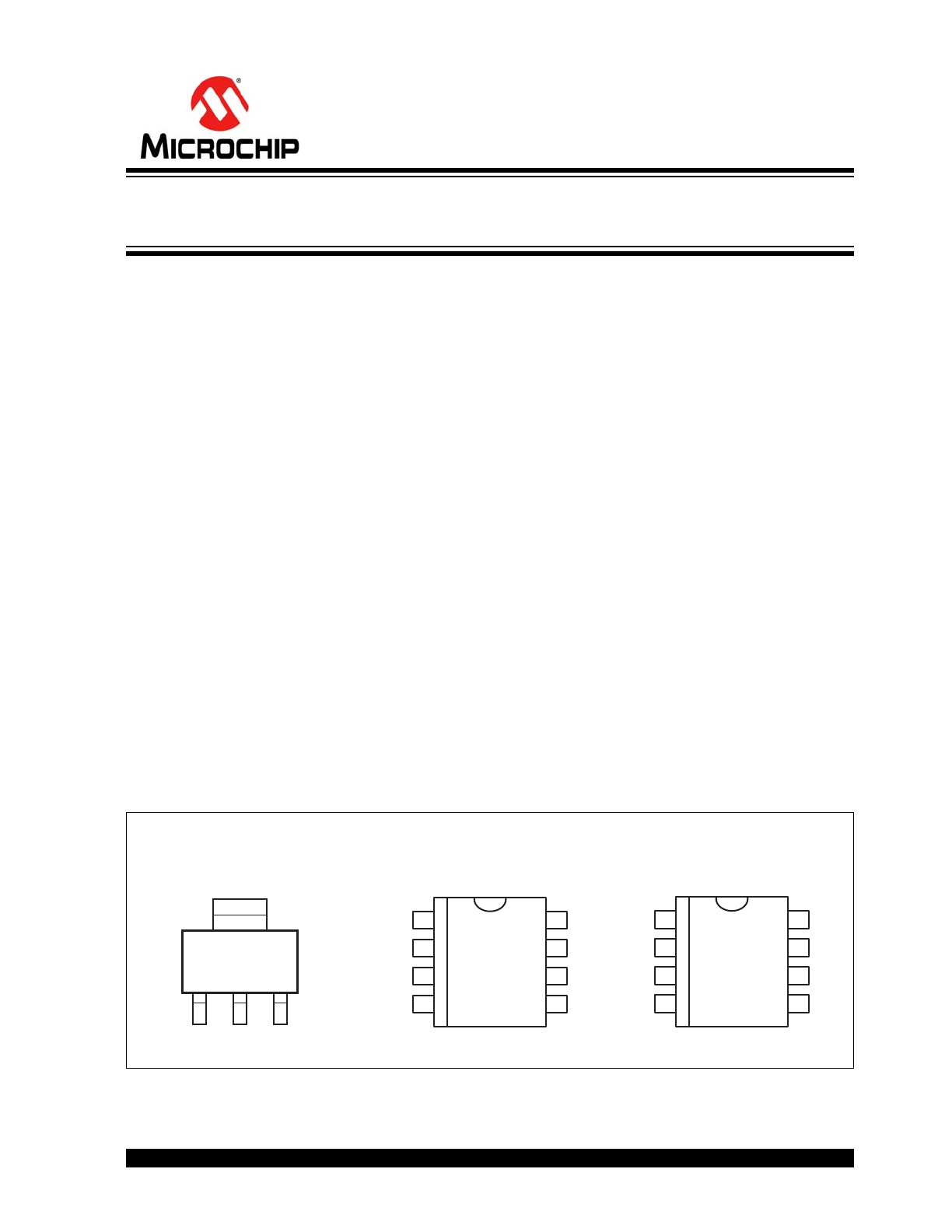
Package Types
MIC39100-
XX
(F
IXED
)
SOT-223 (S)
(Top View)
1
2
3
IN
GND OUT
GND
TAB
MIC39101-
XX
(F
IXED
)
SOIC-8 (M)
(Top View)
MIC39102 (A
DJ
.)
SOIC-8 (M)
(Top View)
1
EN
IN
OUT
FLG
8 GND
GND
GND
GND
7
6
5
2
3
4
1
EN
IN
OUT
ADJ
8 GND
GND
GND
GND
7
6
5
2
3
4
1A, Low Voltage, Low Dropout Regulator
with Reversed-Battery Protection
MIC39100/1/2
DS20005834A-page 2
2017 Microchip Technology Inc.
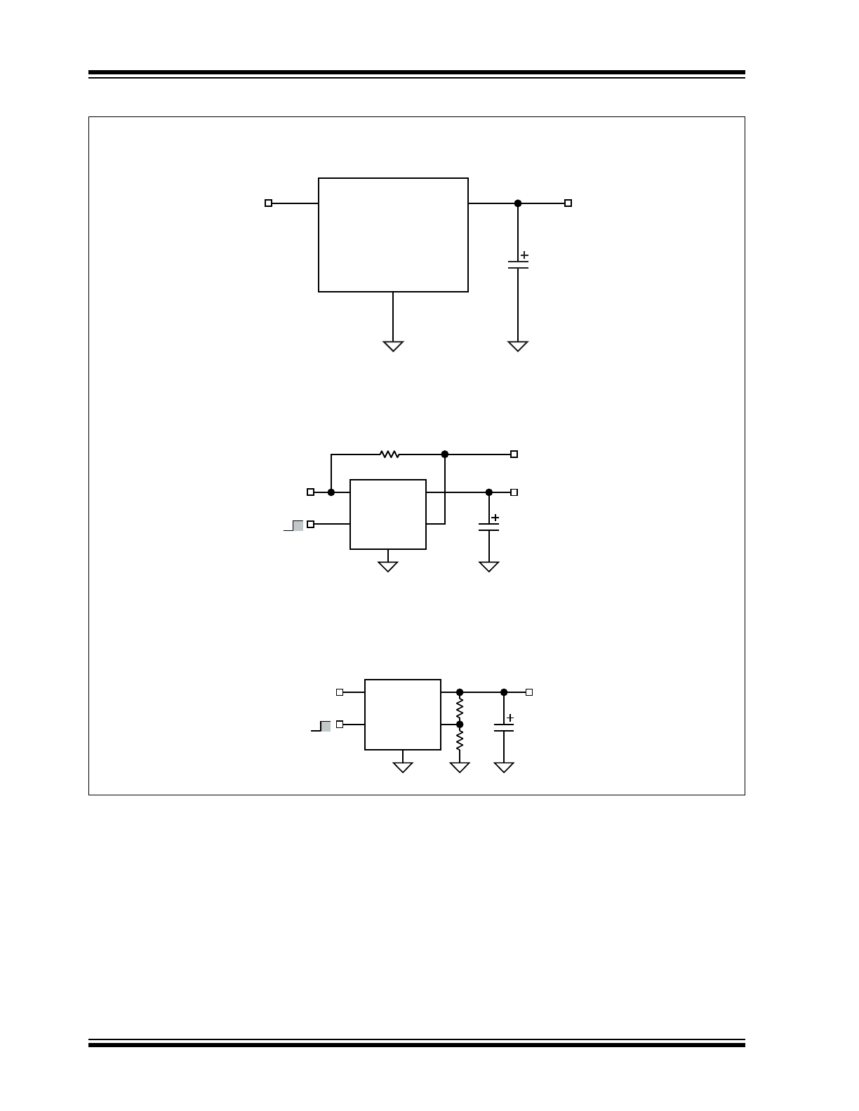
Typical Application Circuits
2.5V/1A Regulator
IN
2.5V
V
IN
3.3V
10μF
TANTALUM
OUT
GND
MIC39100
2.5V/1A Regulator with Error Flag
IN
R1
100k
2.5V
ERROR FLAG
OUTPUT
V
IN
3.3V
10μF
TANTALUM
EN
OUT
FLG
GND
MIC39101
ENABLE
SHUTDOWN
1.5V/1A Adjustable Regulator
IN
R1
1.5V
R2
EN
OUT
ADJ
GND
MIC39102
ENABLE
SHUTDOWN
V
IN
2.5V
10μF
TANTALUM
2017 Microchip Technology Inc.
DS20005834A-page 3
MIC39100/1/2
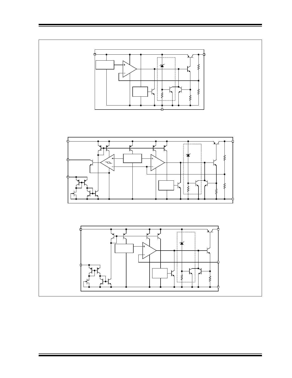
Functional Block Diagrams
18V
O.V. I
LIMIT
1.240V
IN
OUT
GND
MIC39100
REFERENCE
THERMAL
SHUTDOWN
MIC39100 Fixed Regulator
18V
1.240V
1.180V
E N
IN
FL G
GND
OUT
MIC39101
O.V. I
LIMIT
THERMAL
SHUTDOWN
REFERENCE
18V
1.240V
E N
IN
GND
OUT
ADJ
MIC39102
O.V. I
LIMIT
THERMAL
SHUTDOWN
REFERENCE
MIC39101 Fixed Regulator
with Flag and Enable
MIC39102 Adjustable Regulator
MIC39100/1/2
DS20005834A-page 4
2017 Microchip Technology Inc.
1.0
ELECTRICAL CHARACTERISTICS
Absolute Maximum Ratings †
Supply Voltage (V
IN
).................................................................................................................................... –20V to +20V
Enable Voltage (V
EN
) ................................................................................................................................................+20V
ESD Rating ............................................................................................................................................................
Note 1
Maximum Power Dissipation (P
D(MAX)
) ..................................................................................................................
Note 2
Operating Ratings ‡
Supply Voltage (V
IN
)................................................................................................................................. +2.25V to +16V
Enable Voltage (V
EN
) ................................................................................................................................................+16V
†
Notice: Stresses above those listed under “Absolute Maximum Ratings” may cause permanent damage to the device.
This is a stress rating only and functional operation of the device at those or any other conditions above those indicated
in the operational sections of this specification is not intended. Exposure to maximum rating conditions for extended
periods may affect device reliability.
‡ Notice:
The device is not guaranteed to function outside its operating ratings.
Note 1:
Devices are ESD sensitive. Handling precautions are recommended. Human body model, 1.5 kΩ in series
with 100 pF.
2:
P
D(MAX)
= (T
J(MAX)
– T
A
) ÷ θ
JA
, where θ
JA
depends upon the printed circuit layout (see
Application Informa-
tion
).
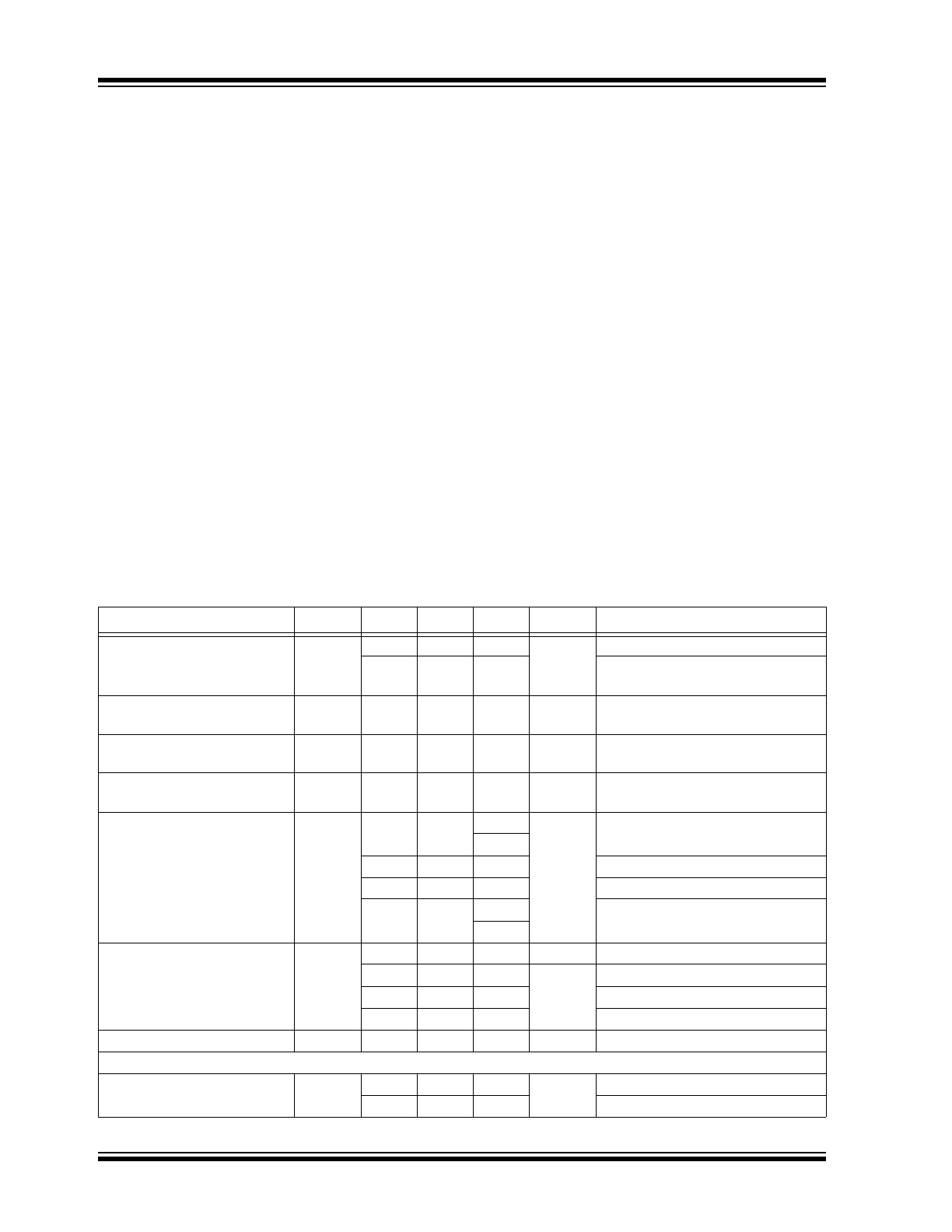
TABLE 1-1:
ELECTRICAL CHARACTERISTICS
Electrical Characteristics:
V
IN
= V
OUT
+ 1V; V
EN
= 2.25V; T
J
= +25°C, bold values indicate –40°C ≤ T
J
≤ +125°C,
unless noted.
Note 1
Parameter
Symbol
Min.
Typ.
Max.
Units
Conditions
Output Voltage
V
OUT
–1
—
1
%
I
OUT
= 10 mA
–2
—
2
10 mA ≤ I
OUT
≤ 1A,
V
OUT
+1V ≤ V
IN
≤ 8V
Line Regulation
—
—
0.06
0.5
%
I
OUT
= 10 mA,
V
OUT
+ 1V ≤ V
IN
≤ 16V
Load Regulation
—
—
0.2
1
%
V
IN
= V
OUT
+ 1V,
10 mA ≤ I
OUT
≤ 1A
Output Voltage Temperature
Coefficient
∆V
OUT
/
∆T
—
40
100
ppm/°C
Note 2
Dropout Voltage,
Note 3
V
DO
—
140
200
mV
I
OUT
= 100 mA, ∆V
OUT
= –1%
250
—
275
—
I
OUT
= 500 mA, ∆V
OUT
= –1%
—
300
500
I
OUT
= 750 mA, ∆V
OUT
= –1%
—
410
550
I
OUT
= 1A, ∆V
OUT
= –1%
630
Ground Current,
Note 4
I
GND
—
400
—
µA
I
OUT
= 100 mA, V
IN
= V
OUT
+ 1V
—
4
—
mA
I
OUT
= 500 mA, V
IN
= V
OUT
+ 1V
—
6.5
—
I
OUT
= 750 mA, V
IN
= V
OUT
+ 1V
—
11
20
I
OUT
= 1A, V
IN
= V
OUT
+ 1V
Current Limit
I
OUT(LIM)
—
1.8
2.5
A
V
OUT
= 0V, V
IN
= V
OUT
+ 1V
Enable Input
Enable Input Voltage
V
EN
—
—
0.8
V
Logic LOW (Off)
2.25
—
—
Logic HIGH (On)
2017 Microchip Technology Inc.
DS20005834A-page 5
MIC39100/1/2
Enable Input Current
I
EN
1
15
30
µA
V
EN
= 2.25V
—
—
75
—
—
2
V
EN
= 0.8V
—
—
4
Flag Output
Output Leakage Voltage
I
FLG(LEAK)
—
0.01
1
µA
V
OH
= 16V
2
Output Low Voltage
V
FLG(DO)
—
210
300
mV
V
IN
= 2.250V, I
OL
= 250 µA,
Note 5
400
Low Threshold
V
FLG
93
—
—
%
% of V
OUT
High Threshold
—
—
99.2
% of V
OUT
Hysteresis
—
1
—
—
MIC39102 Only
Reference Voltage
—
1.228
1.240
1.252
V
I
OUT
= 10 mA
1.215
1.265
1.203
—
1.277
Note 6
Adjust Pin Bias Current
—
—
40
80
nA
—
120
Reference Voltage
Temperature Coefficient
—
—
20
—
ppm/°C —
Adjust Pin Bias Current
Temperature Coefficient
—
—
0.1
—
nA/°C
—
Note 1:
Specification for packaged product only.
2:
Output voltage temperature coefficient is ∆V
OUT(WORST CASE)
÷ (T
J(MAX)
– T
J(MIN)
), where T
J(MAX)
=
+125°C and T
J(MIN)
= –40°C.
3:
V
DO
= V
IN
– V
OUT
when V
OUT
decreases to 99% of its nominal output voltage with V
IN
= V
OUT
+ 1V. For
output voltages below 2.25V, dropout voltage is the input-to-output voltage differential with the minimum
input voltage being 2.25V. Minimum input operating voltage is 2.25V.
4:
I
GND
is the quiescent current (I
IN
= I
GND
+ I
OUT
).
5:
For a 2.5V device, V
IN
= 2.250V (device is in dropout).
6:
V
REF
≤ V
OUT
≤ (V
IN
– 1V), 2.25V ≤ V
IN
≤ 16V, 10 mA ≤ I
L
≤ 1A, T
J
= T
MAX
.
TABLE 1-1:
ELECTRICAL CHARACTERISTICS (CONTINUED)
Electrical Characteristics:
V
IN
= V
OUT
+ 1V; V
EN
= 2.25V; T
J
= +25°C, bold values indicate –40°C ≤ T
J
≤ +125°C,
unless noted.
Note 1
Parameter
Symbol
Min.
Typ.
Max.
Units
Conditions
MIC39100/1/2
DS20005834A-page 6
2017 Microchip Technology Inc.
TEMPERATURE SPECIFICATIONS (
Note 1
)
Parameters
Sym.
Min.
Typ.
Max.
Units
Conditions
Temperature Ranges
Junction Operating Temperature
Range
T
J
–40
—
+125
°C
—
Storage Temperature Range
T
S
–65
—
+150
°C
—
Lead Temperature
—
—
—
+260
°C
Soldering, 5s
Package Thermal Resistances
Thermal Resistance SOT-223
JC
—
15
—
°C/W
—
Thermal Resistance SOIC-8
JC
—
20
—
°C/W
—
Note 1:
The maximum allowable power dissipation is a function of ambient temperature, the maximum allowable
junction temperature and the thermal resistance from junction to air (i.e., T
A
, T
J
,
JA
). Exceeding the
maximum allowable power dissipation will cause the device operating junction temperature to exceed the
maximum +125°C rating. Sustained junction temperatures above +125°C can impact the device reliability.
2017 Microchip Technology Inc.
DS20005834A-page 7
MIC39100/1/2
2.0
TYPICAL PERFORMANCE CURVES
FIGURE 2-1:
Power Supply Rejection
Ratio.
FIGURE 2-2:
Power Supply Rejection
Ratio.
FIGURE 2-3:
Power Supply Rejection
Ratio.
FIGURE 2-4:
Power Supply Rejection
Ratio.
FIGURE 2-5:
Dropout Voltage vs. Output
Current.
FIGURE 2-6:
Dropout Voltage vs.
Temperature.
Note:
The graphs and tables provided following this note are a statistical summary based on a limited number of
samples and are provided for informational purposes only. The performance characteristics listed herein
are not tested or guaranteed. In some graphs or tables, the data presented may be outside the specified
operating range (e.g., outside specified power supply range) and therefore outside the warranted range.
PSRR (dB)
80
60
40
20
0
10
100
1K
10K
100K
1M
V
IN
= 5V
V
OUT
= 3.3V
I
OUT
= 1A
C
OUT
= 10μF
C
IN
= 0μF
FREQUENCY (Hz)
0
20
40
60
80
1E+1 1E+2 1E+3
1E+4
1E+5 1E+6
PSRR (dB)
FREQUENCY (Hz)
V
IN
= 5V
V
OUT
= 3.3V
I
OUT
= 1A
C
OUT
= 47μF
C
IN
= 0μF
10
100
1K
10K
100K
1M
0
20
40
60
80
1E+1 1E+2 1E+3
1E+4
1E+5 1E+6
PSRR (dB)
FREQUENCY (Hz)
V
IN
= 3.3V
V
OUT
= 2.5V
I
OUT
= 1A
C
OUT
= 10μF
C
IN
= 0μF
10
100
1K
10K
100K
1M
0
20
40
60
80
1E+1 1E+2 1E+3
1E+4
1E+5 1E+6
PSRR (dB)
FREQUENCY (Hz)
V
IN
= 3.3V
V
OUT
= 2.5V
I
OUT
= 1A
C
OUT
= 47μF
C
IN
= 0μF
10
100
1K
10K
100K
1M
2.5V
200
300
400
500
1E+2 1E+3
1E+4
1E+5 1E+6
DROPOUT VOLTAGE (mV)
OUTPUT CURRENT (mA)
T
A
= 25°C
0
250
500
750
1000 1250
150
250
350
450
50
0
100
3.3V
1.8V
2.5V
450
500
550
600
DROPOUT VOLTAGE (mV)
TEMPERATURE (°C)
I
LOAD
= 1A
350
300
400
3.3V
1.8V
1E+2 1E+3
1E+4
1E+5
–40 –20 0
20 40 60 80 100 120
MIC39100/1/2
DS20005834A-page 8
2017 Microchip Technology Inc.
FIGURE 2-7:
Dropout Characteristics
(2.5V).
FIGURE 2-8:
Dropout Characteristics
(3.3V).
FIGURE 2-9:
Ground Current vs. Output
Current.
FIGURE 2-10:
Ground Current vs. Supply
Voltage (2.5V).
FIGURE 2-11:
Ground Current vs. Supply
Voltage (2.5V).
FIGURE 2-12:
Ground Current vs. Supply
Voltage (3.3V).
2.2
2.4
2.6
2.8
OUTPUT VOLTAGE (V)
SUPPLY VOLTAGE (V)
I
LOAD
= 100mA
1.8
1.6
2.0
1E+2 1E+3
1E+4
2
2.3
2.6
2.9
3.5
I
LOAD
= 750mA
I
LOAD
= 1A
3.2
1.4
OUTPUT VOLTAGE (V)
SUPPLY VOLTAGE (V)
I
LOAD
= 100mA
I
LOAD
= 750mA
I
LOAD
= 1A
3.2
3.4
3.6
2.8
2.6
3.0
1E+2 1E+3
1E+4
2.8
3.2
3.6
4.0
4.4
2.4
GROUND CURRENT (mA)
OUTPUT CURRENT (mA)
1.8V
3.3V
2.5V
8
10
12
4
2
6
0
200
400
600
800
0
1000
14
GROUND CURRENT (mA)
SUPPLY VOLTAGE (V)
I
LOAD
= 100mA
I
LOAD
= 10mA
0.8
1.0
1.2
0.4
0.2
0.6
0
2
4
6
8
0
2.0
1.4
1.6
1.8
GROUND CURRENT (mA)
SUPPLY VOLTAGE (V)
I
LOAD
= 1A
10
15
5
0
2
4
6
8
0
35
20
25
30
GROUND CURRENT (mA)
SUPPLY VOLTAGE (V)
I
LOAD
= 100mA
I
LOAD
= 10mA
0.8
1.0
1.2
0.4
0.2
0.6
0
2
4
6
8
0
1.4
2017 Microchip Technology Inc.
DS20005834A-page 9
MIC39100/1/2
FIGURE 2-13:
Ground Current vs. Supply
Voltage (3.3V).
FIGURE 2-14:
Ground Current vs.
Temperature.
FIGURE 2-15:
Ground Current vs.
Temperature.
FIGURE 2-16:
Ground Current vs.
Temperature.
FIGURE 2-17:
Output Voltage vs.
Temperature
.
FIGURE 2-18:
Short-Circuit vs.
Temperature
.
GROUND CURRENT (mA)
SUPPLY VOLTAGE (V)
I
LOAD
= 1A
40
50
20
10
30
0
2
4
6
8
0
GROUND CURRENT (mA)
TEMPERATURE (°C)
I
LOAD
= 10mA
0.8
1.0
0.4
0.2
0.6
–40 –20
0
20 40
0
60 80 100 120
3.3V
2.5V
1.8V
GROUND CURRENT (mA)
TEMPERATURE (°C)
I
LOAD
= 500mA
4.5
5.0
3.5
3.0
4.0
–40 –20
0
20 40
2.5
60 80 100 120
3.3V
2.5V
1.8V
1.5
2.0
0.5
1.0
0
GROUND CURRENT (mA)
TEMPERATURE (°C)
I
LOAD
= 1A
15
20
10
–40 –20
0
20 40
60 80 100 120
3.3V
2.5V
1.8V
5
0
OUTPUT VOLTAGE (V)
TEMPERATURE (°C)
3.40
3.30
3.35
–40 –20
0
20 40
60 80 100 120
TYPICAL 3.3V DEVICE
3.25
3.20
SHORT-CIRCUIT CURRENT (A)
TEMPERATURE (°C)
2.5
2.0
–40 –20
0
20 40
1.5
60 80 100 120
3.3V
2.5V
1.8V
0.5
1.0
0
MIC39100/1/2
DS20005834A-page 10
2017 Microchip Technology Inc.
FIGURE 2-19:
Error Flag Voltage vs.
Pull-Up Resistor Value.
FIGURE 2-20:
Enable Current vs.
Temperature.
FIGURE 2-21:
Flag-Low Voltage vs.
Temperature.
FIGURE 2-22:
Load Transient Response.
FIGURE 2-23:
Load Transient Response.
FIGURE 2-24:
Line Transient Response.
FLAG VOLTAGE (V)
RESISTANCE ()
6
5
10
100
1K 10K 100K
4
1M 10M
V
IN
= 5V
FLAG HIGH (OK)
FLAG LOW (FAULT)
2
3
0
1
ENABLE CURRENT (μA)
V
IN
= V
OUT
+ 1V
V
EN
= 2.4V
TEMPERATURE (°C)
12
8
10
–40 –20 0 20 40 60 80 100 120
6
4
140
2
0
FLAG VOLTAGE (mV)
V
IN
= 2.25V
R
PULL-UP
= 22k
TEMPERATURE (°C)
250
150
200
–40 –20 0 20 40 60 80 100 120
100
50
140
0
FLAG-LOW
VOLTAGE
V
OUT
= 2.5V
C
OUT
= 10μF
OUTPUT
VOLTAGE
(200mV/div)
LOAD
CURRENT
(500mA/div)
TIME (250μs/div)
100mA
1A
V
OUT
= 2.5V
C
OUT
= 47μF
OUTPUT
VOLTAGE
(200mV/div)
LOAD
CURRENT
(500mA/div)
TIME (500μs/div)
10mA
1A
V
OUT
= 2.5V
C
OUT
= 10μF
OUTPUT
VOLTAGE
(50mV/div)
INPUT
VOLTAGE
(2V/div)
TIME (25μs/div)