

© 2009 Microchip Technology Inc.
DS22088C-page 1
MCP3422/3/4
Features
• 18-bit
ΔΣ
ADC with Differential Inputs:
- 2 channels: MCP3422 and MCP3423
- 4 channels: MCP3424
• Differential Input Full Scale Range: -V
REF
to
+V
REF
• Self Calibration of Internal Offset and Gain per
Each Conversion
• On-Board Voltage Reference (V
REF
):
- Accuracy: 2.048V ± 0.05%
- Drift: 15 ppm/°C
• On-Board Programmable Gain Amplifier (PGA):
- Gains of 1, 2, 4 or 8
• INL: 10 ppm of Full Scale Range
• Programmable Data Rate Options:
- 3.75 SPS (18 bits)
- 15 SPS (16 bits)
- 60 SPS (14 bits)
- 240 SPS (12 bits)
• One-Shot or Continuous Conversion Options
• Low Current Consumption:
- 135 µA typical
(V
DD
= 3V, Continuous Conversion)
- 36 µA typical
(V
DD
= 3V, One-Shot Conversion with 1 SPS)
• On-Board Oscillator
• I
2
C
™
Interface:
- Standard, Fast and High Speed Modes
- User configurable two external address pins
for MCP3423 and MCP3424
• Single Supply Operation: 2.7V to 5.5V
• Extended Temperature Range: -40°C to +125°C
Typical Applications
• Portable Instrumentation and Consumer Goods
• Temperature Sensing with RTD, Thermistor, and
Thermocouple
• Bridge Sensing for Pressure, Strain, and Force
• Weigh Scales
• Battery Fuel Gauges
• Factory Automation Equipment
Description
The MCP3422, MCP3423 and MCP3424 devices
(MCP3422/3/4) are the low noise and high accuracy
18-Bit delta-sigma analog-to-digital (
ΔΣ A/D) converter
family members of the MCP342X series from Microchip
Technology Inc. These devices can convert analog
inputs to digital codes with up to 18 bits of resolution.
The on-board 2.048V reference voltage enables an
input range of
±
2.048V differentially (full scale
range = 4.096V/PGA).
These devices can output analog-to-digital conversion
results at rates of 3.75, 15, 60, or 240 samples per
second depending on the user controllable
configuration bit settings using the two-wire I
2
C serial
interface. During each conversion, the device
calibrates offset and gain errors automatically. This
provides accurate conversion results from conversion
to conversion over variations in temperature and power
supply fluctuation.
The user can select the PGA gain of x1, x2, x4, or x8
before the analog-to-digital conversion takes place.
This allows the MCP3422/3/4 devices to convert a very
weak input signal with high resolution.
The MCP3422/3/4 devices have two conversion
modes: (a) One-Shot Conversion mode and (b)
Continuous Conversion mode. In One-Shot conversion
mode, the device performs a single conversion and
enters a low current standby mode automatically until it
receives another conversion command. This reduces
current consumption greatly during idle periods. In
Continuous conversion mode, the conversion takes
place continuously at the set conversion speed. The
device updates its output buffer with the most recent
conversion data.
The devices operate from a single 2.7V to 5.5V power
supply and have a two-wire I
2
C compatible serial
interface for a standard (100 kHz), fast (400 kHz), or
high-speed (3.4 MHz) mode.
The I
2
C address bits for the MCP3423 and MCP3424
are selected by using two external I
2
C address
selection pins (Adr0 and Adr1). The user can configure
the device to one of eight available addresses by
connecting these two address selection pins to V
DD
,
V
SS
or float. The I
2
C address bits of the MCP3422 are
programmed at the factory during production.
18-Bit, Multi-Channel
ΔΣ Analog-to-Digital Converter with
I
2
C™ Interface and On-Board Reference
MCP3422/3/4
DS22088C-page 2
© 2009 Microchip Technology Inc.
The MCP3422 and MCP3423 devices have two
differential input channels and the MCP3424 has four-
differential input channels. All electrical properties of
these three devices are the same except the
differences in the number of input channels and I
2
C
address bit selection options.
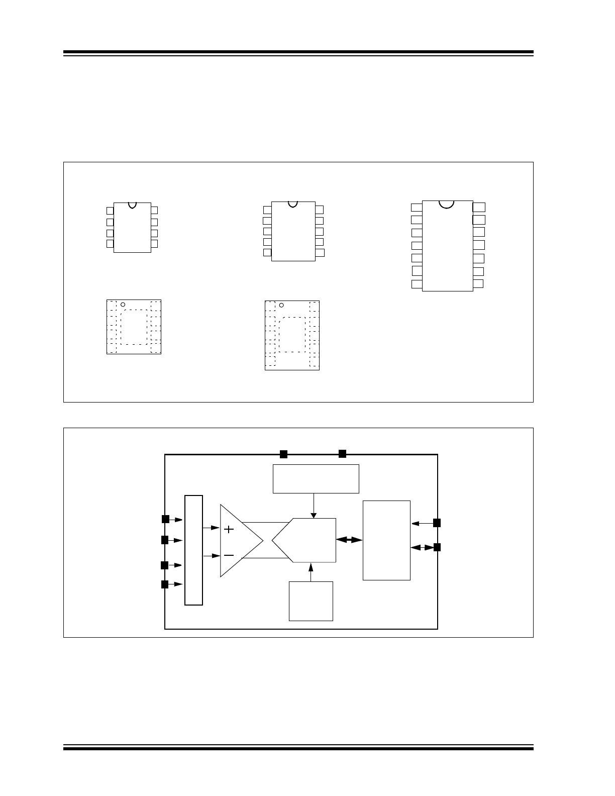
The MCP3422 is available in 8-pin SOIC, DFN, and
MSOP packages. The MCP3423 is available in 10-pin
DFN, and MSOP packages. The MCP3424 is available
in 14-pin SOIC and TSSOP packages.
Package Types
Functional Block Diagram
4
5
6
9
CH2-
V
SS
CH3+
Adr1
Adr0
3
12
CH2+
CH3-
2
13
CH1-
CH4+
1
14
CH1+
CH4-
7
8
SDA
SCL
V
DD
11
10
2
3
4
7
8
9
CH1-
V
DD
SDA
Adr0
V
SS
SCL
1
10
CH1+
Adr1
5
6
CH2-
CH2+
2
3
4
5
6
7
CH1-
V
DD
SDA
CH2+
V
SS
SCL
1
8
CH1+
CH2-
MCP3422
2x3 DFN*
V
DD
CH1-
SDA
CH2+
V
SS
1
2
3
4
8
7
6
5 SCL
CH2-
CH1+
* Includes Exposed Thermal Pad (EP); see
Table 3-1
.
EP
9
MCP3423
3x3 DFN*
V
SS
CH1-
CH2+
Adr0
SCL
1
2
3
4
10
9
8
7 SDA
Adr1
CH1+
EP
11
CH2-
5
6 V
DD
MCP3422
MCP3422
MSOP, SOIC
MC
P
3
423
MC
P
3
424
MCP3423
MSOP
MCP3424
SOIC, TSSOP
V
SS
V
DD
PGA
SCL
SDA
MUX
I
2
C
Interface
Gain = 1,2,4, or 8
Voltage Reference
Clock
(2.048V)
V
REF
ΔΣ ADC
Converter
Oscillator
CH1+
CH1-
CH2+
CH2-
MCP3422
© 2009 Microchip Technology Inc.
DS22088C-page 3
MCP3422/3/4
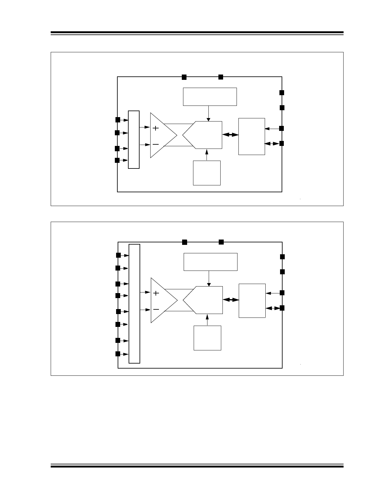
Functional Block Diagram
Functional Block Diagram
V
SS
V
DD
CH1+
CH1-
PGA
SCL
SDA
MUX
I
2
C
Interface
Gain = 1,2,4, or 8
Adr1
Adr0
CH2+
CH2-
Voltage Reference
Clock
(2.048V)
V
REF
ΔΣ ADC
Converter
Oscillator
MCP3423
V
SS
V
DD
CH1+
CH1-
PGA
SCL
SDA
MUX
I
2
C
Interface
Gain = 1,2,4, or 8
Adr1
Adr0
CH2+
CH2-
CH3+
CH3-
CH4+
CH4-
Voltage Reference
Clock
(2.048V)
V
REF
ΔΣ ADC
Converter
Oscillator
MCP3424

MCP3422/3/4
DS22088C-page 4
© 2009 Microchip Technology Inc.
NOTES:
© 2009 Microchip Technology Inc.
DS22088C-page 5
MCP3422/3/4
1.0
ELECTRICAL
CHARACTERISTICS
Absolute Maximum Ratings†
V
DD
...................................................................................7.0V
All inputs and outputs ............. ..........V
SS
–0.4V to V
DD
+0.4V
Differential Input Voltage ...................................... |V
DD
- V
SS
|
Output Short Circuit Current ................................ Continuous
Current at Input Pins ....................................................±2 mA
Current at Output and Supply Pins ............................±10 mA
Storage Temperature ....................................-65°C to +150°C
Ambient Temp. with power applied ...............-55°C to +125°C
ESD protection on all pins
................ ≥ 6 kV HBM, ≥ 400V MM
Maximum Junction Temperature (T
J
) . .........................+150°C
†Notice: Stresses above those listed under “Maximum Rat-
ings” may cause permanent damage to the device. This is a
stress rating only and functional operation of the device at
those or any other conditions above those indicated in the
operational listings of this specification is not implied.
Exposure to maximum rating conditions for extended periods
may affect device reliability
.
ELECTRICAL CHARACTERISTICS
Electrical Specifications: Unless otherwise specified, all parameters apply for T
A
= -40°C to +85°C, V
DD
= +5.0V, V
SS
= 0V,
CHn+ = CHn- = V
REF
/2, V
INCOM
= V
REF
/2. All ppm units use 2*V
REF
as differential full scale range.
Parameters
Sym
Min
Typ
Max
Units
Conditions
Analog Inputs
Differential Full Scale Input
Voltage Range
FSR
—
±2.048/PGA
—
V
V
IN
= [CHn+ - CHn-]
Maximum Input Voltage Range
V
SS
-0.3
—
V
DD
+0.3
V
(Note 1)
Differential Input Impedance
Z
IND
(f)
—
2.25/PGA
—
M
Ω
During normal mode operation
(Note 2)
Common Mode input
Impedance
Z
INC
(f)
—
25
—
M
Ω
PGA = 1, 2, 4, 8
System Performance
Resolution and No Missing
Codes
(Effective Number of Bits)
(Note 3)
12
—
—
Bits
DR = 240 SPS
14
—
—
Bits
DR = 60 SPS
16
—
—
Bits
DR = 15 SPS
18
—
—
Bits
DR = 3.75 SPS
Data Rate
(Note 4)
DR
176
240
328
SPS
12 bits mode
44
60
82
SPS
14 bits mode
11
15
20.5
SPS
16 bits mode
2.75
3.75
5.1
SPS
18 bits mode
Output Noise
—
1.5
—
µV
RMS
T
A
= +25°C, DR = 3.75 SPS,
PGA = 1, V
IN
+ = V
IN
- = GND
Integral Non-Linearity
INL
—
10
35
ppm of
FSR
DR = 3.75 SPS, FSR = Full
Scale Range (Note 5)
Internal Reference Voltage
V
REF
—
2.048
—
V
Gain Error (Note 6)
—
0.05
0.35
%
PGA = 1, DR = 3.75 SPS
Note
1:
Any input voltage below or greater than this voltage causes leakage current through the ESD diodes at the input pins.
This parameter is ensured by characterization and not 100% tested.
2:
This input impedance is due to 3.2 pF internal input sampling capacitor.
3:
This parameter is ensured by design and not 100% tested.
4:
The total conversion speed includes auto-calibration of offset and gain.
5:
INL is the difference between the endpoints line and the measured code at the center of the quantization band.
6:
Includes all errors from on-board PGA and V
REF
.
7:
This parameter is ensured by characterization and not 100% tested.
8:
MCP3423 and MCP3424 only.
9:
Addr_Float voltage is applied at address pin.
10: No voltage is applied at address pin (left “floating”).
MCP3422/3/4
DS22088C-page 6
© 2009 Microchip Technology Inc.
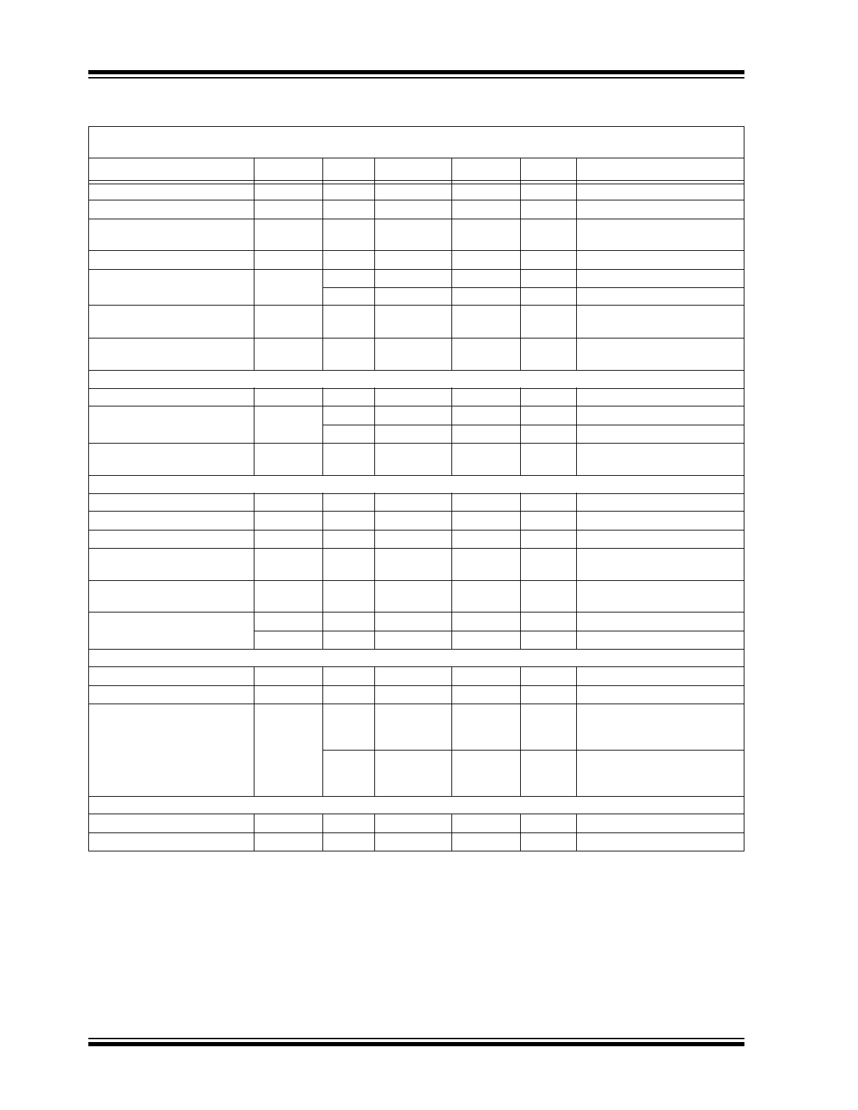
PGA Gain Error Match (Note 6)
—
0.1
—
%
Between any 2 PGA settings
Gain Error Drift (Note 6)
—
15
—
ppm/°C
PGA=1, DR=3.75 SPS
Offset Error
V
OS
—
15
55
µV
Tested at PGA = 1
DR = 3.75 SPS
Offset Drift vs. Temperature
—
50
—
nV/°C
Common-Mode Rejection
—
105
—
dB
at DC and PGA =1,
—
110
—
dB
at DC and PGA =8, T
A
= +25°C
Gain vs. V
DD
—
5
—
ppm/V
T
A
= +25°C, V
DD
= 2.7V to 5.5V,
PGA = 1
Power Supply Rejection at DC
Input
—
100
—
dB
T
A
= +25°C, V
DD
= 2.7V to 5.5V,
PGA = 1
Power Requirements
Voltage Range
V
DD
2.7
—
5.5
V
Supply Current during
Conversion
I
DDA
—
145
180
µA
V
DD
= 5.0V
—
135
—
µA
V
DD
= 3.0V
Supply Current during Standby
Mode
I
DDS
—
0.3
1
µA
V
DD
= 5.0V
I
2
C Digital Inputs and Digital Outputs
High level input voltage
V
IH
0.7V
DD
—
V
DD
V
at SDA and SCL pins
Low level input voltage
V
IL
—
—
0.3V
DD
V
at SDA and SCL pins
Low level output voltage
V
OL
—
—
0.4
V
I
OL
= 3 mA
Hysteresis of Schmidt Trigger
for inputs (Note 7)
V
HYST
0.05V
DD
—
—
V
f
SCL
= 100 kHz
Supply Current when I
2
C bus
line is active
I
DDB
—
—
10
µA
Device is in standby mode while
I
2
C bus is active
Input Leakage Current
I
ILH
—
—
1
µA
V
IH
= 5.5V
I
ILL
-1
—
—
µA
V
IL
= GND
Logic Status of I
2
C Address Pins (Note 8)
Adr0 and Adr1 Pins
Addr_Low
V
SS
—
0.2V
DD
V
The device reads logic low.
Adr0 and Adr1 Pins
Addr_High
0.75V
DD
—
V
DD
V
The device reads logic high.
Adr0 and Adr1 Pins
Addr_Float
0.35V
DD
—
0.6V
DD
V
Read pin voltage if voltage is
applied to the address pin.
(Note 9)
—
V
DD
/2
—
Device outputs float output
voltage (V
DD
/2) on the address
pin, if left “floating”. (Note 10)
Pin Capacitance and I
2
C Bus Capacitance
Pin capacitance
C
PIN
—
4
10
pF
I
2
C Bus Capacitance
C
b
—
—
400
pF
ELECTRICAL CHARACTERISTICS (CONTINUED)
Electrical Specifications: Unless otherwise specified, all parameters apply for T
A
= -40°C to +85°C, V
DD
= +5.0V, V
SS
= 0V,
CHn+ = CHn- = V
REF
/2, V
INCOM
= V
REF
/2. All ppm units use 2*V
REF
as differential full scale range.
Parameters
Sym
Min
Typ
Max
Units
Conditions
Note
1:
Any input voltage below or greater than this voltage causes leakage current through the ESD diodes at the input pins.
This parameter is ensured by characterization and not 100% tested.
2:
This input impedance is due to 3.2 pF internal input sampling capacitor.
3:
This parameter is ensured by design and not 100% tested.
4:
The total conversion speed includes auto-calibration of offset and gain.
5:
INL is the difference between the endpoints line and the measured code at the center of the quantization band.
6:
Includes all errors from on-board PGA and V
REF
.
7:
This parameter is ensured by characterization and not 100% tested.
8:
MCP3423 and MCP3424 only.
9:
Addr_Float voltage is applied at address pin.
10: No voltage is applied at address pin (left “floating”).
© 2009 Microchip Technology Inc.
DS22088C-page 7
MCP3422/3/4
TEMPERATURE CHARACTERISTICS
Electrical Specifications: Unless otherwise indicated,
T
A
= -40°C to +125°C, V
DD
= +5.0V, V
SS
= 0V.
Parameters
Sym
Min
Typ
Max
Units
Conditions
Temperature Ranges
Specified Temperature Range
T
A
-40
—
+85
°C
Operating Temperature Range
T
A
-40
—
+125
°C
Storage Temperature Range
T
A
-65
—
+150
°C
Thermal Package Resistances
Thermal Resistance, 8L-DFN (2x3)
θ
JA
—
68
—
°C/W
Thermal Resistance, 8L-MSOP
θ
JA
—
211
—
°C/W
Thermal Resistance, 8L-SOIC
θ
JA
—
149.5
—
°C/W
Thermal Resistance, 10L-DFN (3x3)
θ
JA
—
53.3
—
°C/W
Thermal Resistance, 10L-MSOP
θ
JA
—
202
—
°C/W
Thermal Resistance, 14L-SOIC
θ
JA
—
95.3
—
°C/W
Thermal Resistance, 14L-TSSOP
θ
JA
—
100
—
°C/W

MCP3422/3/4
DS22088C-page 8
© 2009 Microchip Technology Inc.
NOTES:
© 2009 Microchip Technology Inc.
DS22088C-page 9
MCP3422/3/4
2.0
TYPICAL PERFORMANCE CURVES
Note: Unless otherwise indicated, T
A
= -40°C to +85°C, V
DD
= +5.0V, V
SS
= 0V, CHn+ = CHn- = V
REF
/2,
V
INCOM
= V
REF
/2.
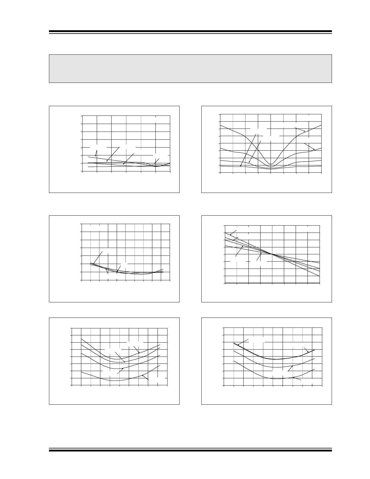
FIGURE 2-1:
INL vs. Supply Voltage
(V
DD
).
FIGURE 2-2:
INL vs. Temperature.
FIGURE 2-3:
Offset Error vs.
Temperature.
FIGURE 2-4:
Output Noise vs. Input
Voltage.
FIGURE 2-5:
Total Error vs. Input Voltage.
FIGURE 2-6:
Gain Error vs. Temperature.
Note:
The graphs and tables provided following this note are a statistical summary based on a limited number of
samples and are provided for informational purposes only. The performance characteristics listed herein
are not tested or guaranteed. In some graphs or tables, the data presented may be outside the specified
operating range (e.g., outside specified power supply range) and therefore outside the warranted range.
0
0.0005
0.001
0.0015
0.002
0.0025
0.003
0.0035
2.5
3
3.5
4
4.5
5
5.5
V
DD
(V)
In
te
gr
a
l N
on-
Li
n
e
a
ri
ty
(%
of
FS
R)
PGA = 8
PGA = 4
PGA = 1
PGA = 2
T
A
= +25°C
0
0.0005
0.001
0.0015
0.002
0.0025
0.003
0.0035
-60 -40 -20
0
20
40
60
80 100 120 140
Temperature (
o
C)
In
te
g
ra
l N
o
n-
Li
ne
a
ri
ty
(%
o
f F
S
R
)
2.7V
5V
5.5V
PGA = 1
-20
-15
-10
-5
0
5
10
15
20
-60 -40 -20
0
20
40
60
80 100 120 140
Temperature (°C)
O
ff
s
e
t E
rror (
µ
V
)
PGA = 1
PGA = 2
PGA = 4
PGA = 8
0
1
2
3
4
5
6
7
8
-100
-75
-50
-25
0
25
50
75
100
Input Signal (% of FSR)
Ou
tP
u
t N
o
is
e
(µ
V,
rm
s)
PGA = 1
PGA = 2
PGA = 4
PGA = 8
T
A
= +25°C
-2
-1.5
-1
-0.5
0
0.5
1
1.5
2
-100
-75
-50
-25
0
25
50
75
100
Input Voltage (% of Full-Scale)
T
o
ta
l E
rro
r (
m
V
)
PGA = 1
PGA = 8
PGA = 4
PGA = 2
T
A
= +25°C
-0.6
-0.5
-0.4
-0.3
-0.2
-0.1
0
0.1
0.2
-60 -40 -20
0
20
40
60
80 100 120 140
Temperature (°C)
G
a
in
E
rro
r (
%
o
f F
S
R
)
PGA = 1
PGA = 2
PGA = 4
PGA = 8
MCP3422/3/4
DS22088C-page 10
© 2009 Microchip Technology Inc.
Note: Unless otherwise indicated, T
A
= -40°C to +85°C, V
DD
= +5.0V, V
SS
= 0V, CHn+ = CHn- = V
REF
/2,
V
INCOM
= V
REF
/2.
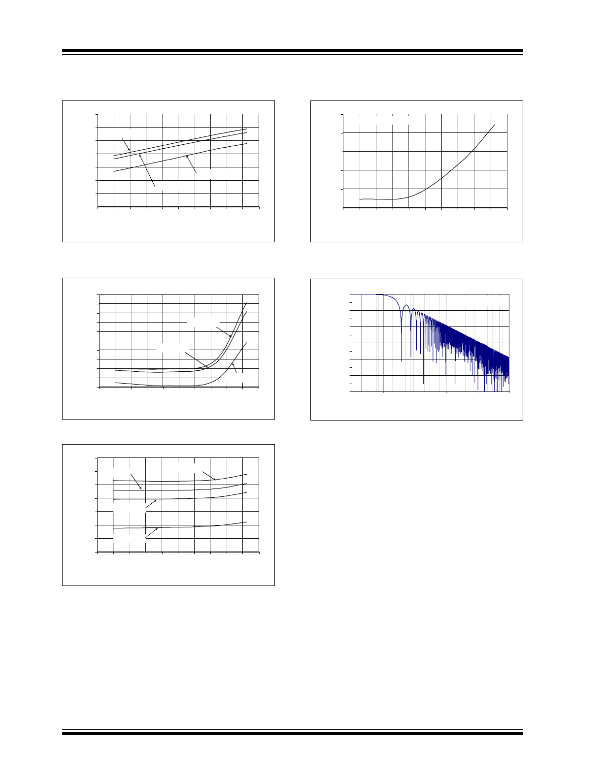
FIGURE 2-7:
I
DDA
vs. Temperature.
FIGURE 2-8:
I
DDS
vs. Temperature.
FIGURE 2-9:
I
DDB
vs. Temperature.
FIGURE 2-10:
Oscillator Drift vs.
Temperature.
FIGURE 2-11:
Frequency Response.
60
80
100
120
140
160
180
200
-60
-40
-20
0
20
40
60
80
100 120 140
Temperature (°C)
I
DD
A
(µ
A
)
V
DD
= 5.5V
V
DD
= 5.0V
V
DD
= 2.7V
0
0.1
0.2
0.3
0.4
0.5
0.6
0.7
0.8
0.9
1
-60 -40 -20
0
20
40
60
80 100 120 140
Temperature (°C)
I
DD
S
(µA
)
V
DD
= 2.7V
V
DD
= 5.0V
V
DD
= 5.5V
0
2
4
6
8
10
12
14
-60
-40
-20
0
20
40
60
80
100 120 140
Temperature (°C)
I
DD
B
(µ
A
)
V
DD
= 5.5V
V
DD
= 5.0V
V
DD
= 4.5V
V
DD
= 2.7V
-2
-1
0
1
2
3
-60
-40
-20
0
20
40
60
80
100 120 140
Temperature (°C)
O
s
c
illa
to
r Drif
t (
%
)
Data Rate = 3.75 SPS
Data Rate = 3.75 SPS
-120
-110
-100
-90
-80
-70
-60
-50
-40
-30
-20
-10
0
0.1
1
10
100
1000
10000
Input Signal Frequency (Hz)
M
a
gni
tu
de
(dB
)
0.1
1
10
100
1k
10k