
2016 Microchip Technology Inc.
DS20005428A-page 1
Features
• High-Voltage CMOS technology
• Symmetric row drive (reduces latent imaging in
ACTFEL displays)
• Output voltage up to +230V
• Low power level shifting
• Source/sink current minimum 70 mA
• Shift register speed 4.0 MHz
• Pin-programmable shift direction
Description
HV7022 is a low-voltage serial to high-voltage parallel
converter with push-pull outputs. It is especially suited
for use as a symmetric row driver in AC thin-film elec-
troluminescent (ACTFEL) displays. HV7022 offers 34
output lines, a direction (DIR) pin to give CW or CCW
shift register loading, output enable (OE), and polarity
(POL) control. After data is entered on the falling edge
of CLK, a logic high will cause the output to swing to
V
PP
if POL is high, or to GND if POL is low.
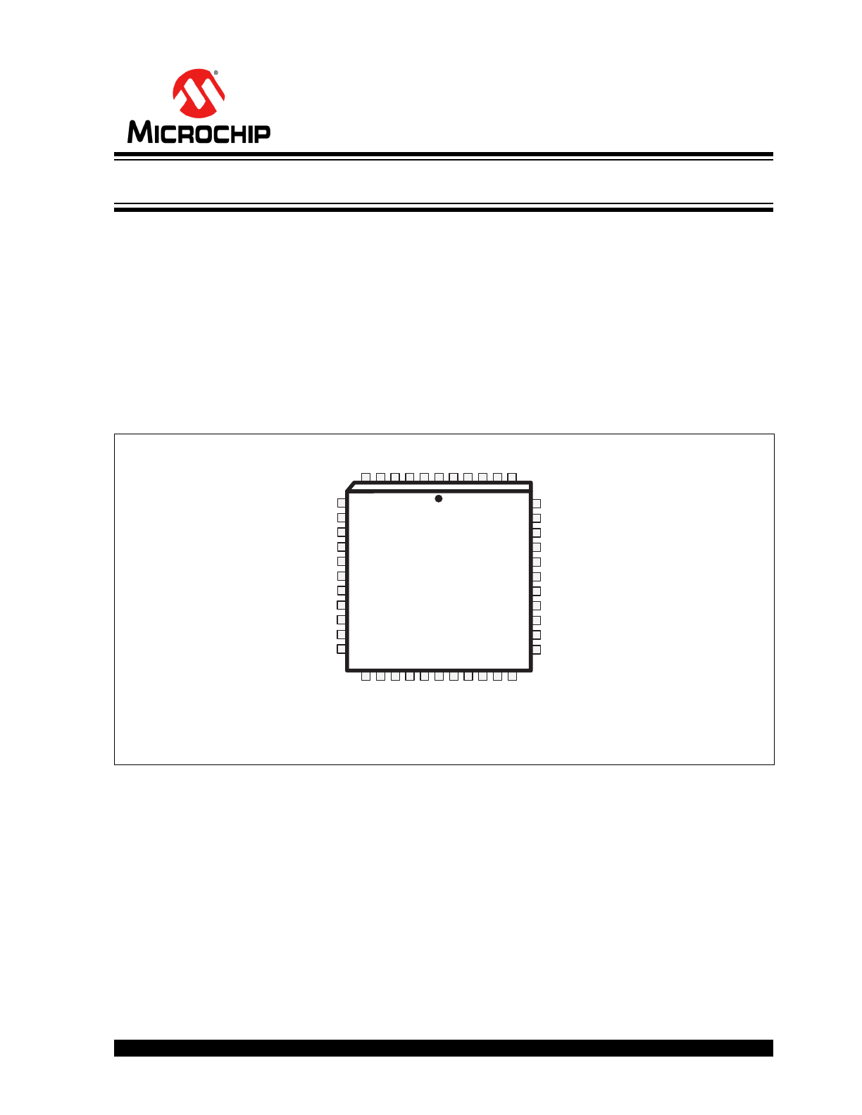
Package Type
44-Lead PLCC
See
Table 2-1
for pin information
1 44
6
40
HV7022
34-Channel Symmetric Row Driver
HV7022
DS20005428A-page 2
2016 Microchip Technology Inc.
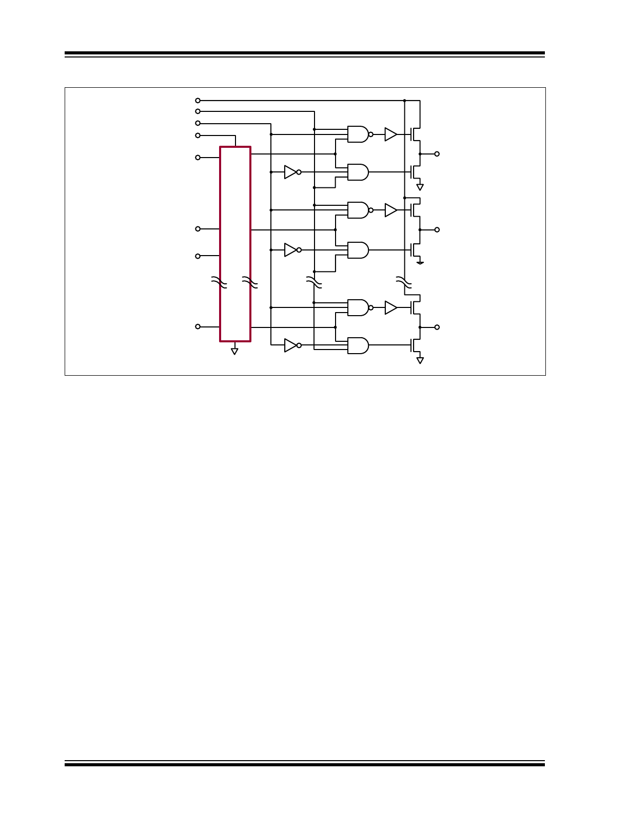
Functional Block Diagram
HV
OUT
1
OE
POL
DATA INPUT
DATA OUT
GND
S/R
CLK
VDD
VPP
DIR
HV
OUT
2
HV
OUT
34
Level
Translator
P
N
P
N
P
N
Level
Translator
Level
Translator

2016 Microchip Technology Inc.
DS20005428A-page 3
HV7022
1.0
ELECTRICAL CHARACTERISTICS
ABSOLUTE MAXIMUM RATINGS
†
Supply voltage, V
DD
...................................................................................................................................-0.3V to +15V
Supply voltage, V
PP
.................................................................................................................................-0.3V to +250V
Logic input levels ............................................................................................................................... -0.3V to V
DD
+0.3V
Ground current
1
....................................................................................................................................................... 1.5A
Continuous total power dissipation
2
.................................................................................................................. 1200mW
Operating temperature range.................................................................................................................. -40°C to +85°C
Storage temperature range ................................................................................................................... -65°C to +150°C
1: Duty cycle is limited by the total power dissipated in the package.
2: For operation above 25°C ambient derate linearly to maximum operating temperature at 25 mW/°C.
† Notice: Stresses above those listed under “Maximum Ratings” may cause permanent damage to the device. This is
a stress rating only and functional operation of the device at those or any other conditions above those indicated in the
operational listings of this specification is not implied. Exposure to maximum rating conditions for extended periods
may affect device reliability.
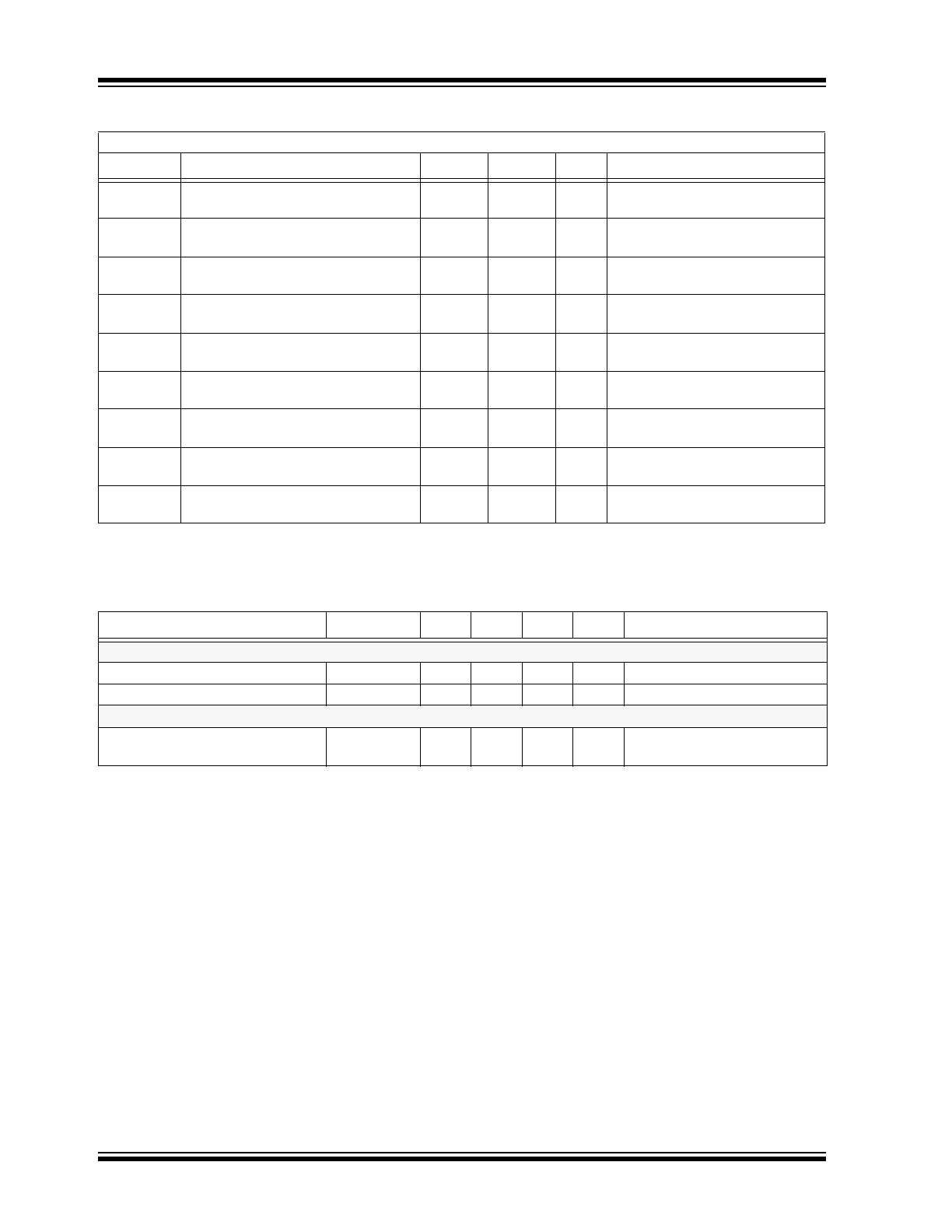
ELECTRICAL CHARACTERISTICS
Recommended Operating Conditions: V
PP
= 230V, V
DD
= 12V, T
A
= 25°C, unless otherwise noted
Symbol
Parameter
Min
Max
Units Conditions
DC Characteristics
I
DD
V
DD
supply current
-
10
mA
f
CLK
= 4.0MHz, V
DD
=13.2V
I
PP
V
PP
supply current
-
4.0
mA
One output high (
Note 1
)
-
100
µA
All outputs low or High-Z
-
750
All outputs low or High-Z (125°C)
I
DDQ
Quiescent V
DD
supply current
-
100
µA
All V
IN
= GND or V
DD
V
OH
High-level output
HV
OUT
195
-
V
I
O
= -70mA
DATA OUT
11
-
V
I
O
= -500µA
V
OL
Low-level output
HV
OUT
-
30
V
I
O
= +70mA
DATA OUT
-
1.0
V
I
O
= +500µA
I
IH
High-level logic input current
-
1.0
µA
V
IH
= 12V
I
IL
Low-level logic input current
-
-1.0
µA
V
IL
= 0V
AC Characteristics
f
CLK
Clock frequency
-
4.0
MHz
–
t
WH
,t
WL
Pulse duration clock width high or low
125
-
ns
–
t
SUD
Data set-up time before falling clock
100
-
ns
–
t
HD
Data hold time after falling clock
100
-
ns
–
t
SUC
Setup time clock low before V
PP
↑ or
GND↓
300
-
ns
–
t
SUE
Setup time enable high before V
PP
↑
or GND↓
300
-
ns
–
t
SUP
Setup time polarity high or low before
V
PP
↑ or GND↓
300
-
ns
–
t
HC
Hold time clock high after V
PP
↑ or
GND↓
500
-
ns
–
t
HE
Hold time enable high after V
PP
↑ or
GND↓
300
-
ns
–
t
HP
Hold time polarity high or low after
V
PP
↑ or GND↓
300
-
ns
–
HV7022
DS20005428A-page 4
2016 Microchip Technology Inc.
Note 1: The total number of ON outputs times the duty cycle must not exceed the allowable package power dissi-
pation.
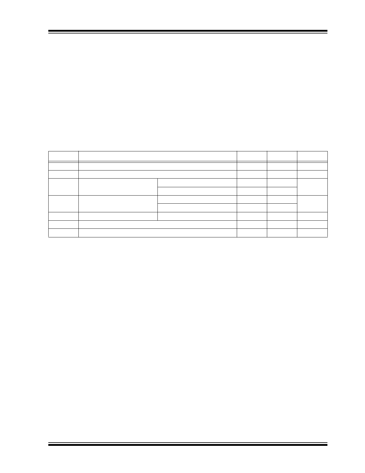
t
DHL
Delay time high to low-level output
from clock
-
150
ns
C
L
= 10pF
t
DLH
Delay time low to high-level output
from clock
-
200
ns
C
L
= 10pF
t
THL
Transition time high to low-level
serial output
-
200
ns
C
L
= 15pF
t
TLH
Transition time low to high-level
serial output
-
100
ns
C
L
= 15pF
t
ONH
High-level turn-on time HV
OUT
from
enable
-
500
ns
V
OH
= 195V, R
L
= 2.0kΩ to 95V
t
ONL
Low-level turn-on time HV
OUT
from
enable
-
500
ns
V
OH
= 130V, R
L
= 2.0kΩ to 30V
t
OFFH
High-level turn-off time HV
OUT
from
enable
-
1000
ns
V
OH
= 195V, R
L
= 2.0kΩ to 95V
t
OFFL
Low-level turn-off time HV
OUT
from
enable
-
500
ns
V
OH
= 130V, R
L
= 2.0kΩ to 30V
SR
Slew rate, V
PP
or GND
-
45
V/µs
One active output driving 4.7nF
load to V
PP
or GND
TEMPERATURE SPECIFICATIONS
Parameter
Symbol
Min
Typ
Max
Units Conditions
Temperature Ranges
Operating Temperature
–
-40
–
85
°C
–
Storage Temperature
–
-65
–
150
°C
–
Package Thermal Resistances
Thermal Resistance, 44-Lead
PLCC
θ
ja
–
37
–
°C/W
–
ELECTRICAL CHARACTERISTICS (CONTINUED)
Recommended Operating Conditions: V
PP
= 230V, V
DD
= 12V, T
A
= 25°C, unless otherwise noted
Symbol
Parameter
Min
Max
Units Conditions
2016 Microchip Technology Inc.
DS20005428A-page 5
HV7022
1.1
Power up and Recommended
Operating Conditions
To power-up HV7022, perform the following power-up
sequence:
1.
Connect ground
2.
Apply V
DD
3.
Set all inputs (Data, CLK, Enable, etc) to a
known state.
4.
Apply V
PP
(V
PP
should not drop below V
DD
or
float during operation).
To power-down the device, reverse the steps above.
RECOMMENDED OPERATING CONDITIONS
Symbol
Parameter
Min
Max
Units
V
DD
Logic supply voltage
10.8
13.2
V
V
PP
High voltage supply
–
230
V
V
IH
High-level input voltage
V
DD
= 10.8
8.1
–
V
V
DD
= 13.2
9.9
–
V
IL
Low-level input voltage
V
DD
= 10.8
-
2.7
V
V
DD
= 13.2
-
3.3
f
CLK
Clock frequency
-
4.0
MHz
T
A
Operating free-air temperature
-40
+85
°C
I
OD
Allowable pulsed current through output diode.
–
±300
mA
HV7022
DS20005428A-page 6
2016 Microchip Technology Inc.
2.0
PIN DESCRIPTION
The locations of the pins are listed in
Package Type
.
TABLE 2-1:
PIN DESCRIPTION
Pin #
HV7022
Description
1
HV
OUT
18/17
High voltage outputs.
2
HV
OUT
17/18
3
HV
OUT
16/19
4
HV
OUT
15/20
5
HV
OUT
14/21
6
HV
OUT
13/22
7
HV
OUT
12/23
8
HV
OUT
11/24
9
HV
OUT
10/25
10
HV
OUT
9/26
11
HV
OUT
8/27
12
HV
OUT
7/28
13
HV
OUT
6/29
14
HV
OUT
5/30
15
HV
OUT
4/31
16
HV
OUT
3/32
17
HV
OUT
2/33
18
HV
OUT
1/34
19
Data OUT
Serial data output.
Data output for cascading to the data input of the next device.
20
OE
Output enable input.
When OE is Low, all HV outputs are forced into a High-Z state, regardless of
data in each channel. When OE is High, all HV outputs reflect data latched.
21
CLK
Data shift register clock
Input are shifted into the shift register on the negative edge of the clock.
22
GND
Logic and high voltage ground.
23
DIR
Direction.
24
VDD
Low voltage logic power rail.
25
POL
Polarity.
26
DATA INPUT
Serial data input.
Data needs to be present before each falling edge of the clock.
27
VPP
High voltage power rail.
28
NC
No Connect.
29
HV
OUT
34/1
High voltage outputs
30
HV
OUT
33/2
31
HV
OUT
32/3
32
HV
OUT
31/4
33
HV
OUT
30/5
34
HV
OUT
29/6
2016 Microchip Technology Inc.
DS20005428A-page 7
HV7022
Note 1: Pin designation for DIR H/L
Example: for DIR = H, pin 1 is HV
OUT
18
for DIR = L, pin 1 is HV
OUT
17
35
HV
OUT
28/7
High voltage outputs.
36
HV
OUT
27/8
37
HV
OUT
26/9
38
HV
OUT
25/10
39
HV
OUT
24/11
40
HV
OUT
23/12
41
HV
OUT
22/13
42
HV
OUT
21/14
43
HV
OUT
20/15
44
HV
OUT
19/16
TABLE 2-1:
PIN DESCRIPTION
Pin #
HV7022
Description
HV7022
DS20005428A-page 8
2016 Microchip Technology Inc.
3.0
FUNCTIONAL DESCRIPTION
Table 3-1
provides functional information about HV7022.
Note 1: H = logic high level, L = logic low level, X = irrelevant, ↓ = high-to-low transition
Q1 = HV
OUT
1, Qn = HV
OUT
n, etc.
* = dependent on previous state and whether an O/P or S/R command occurred.
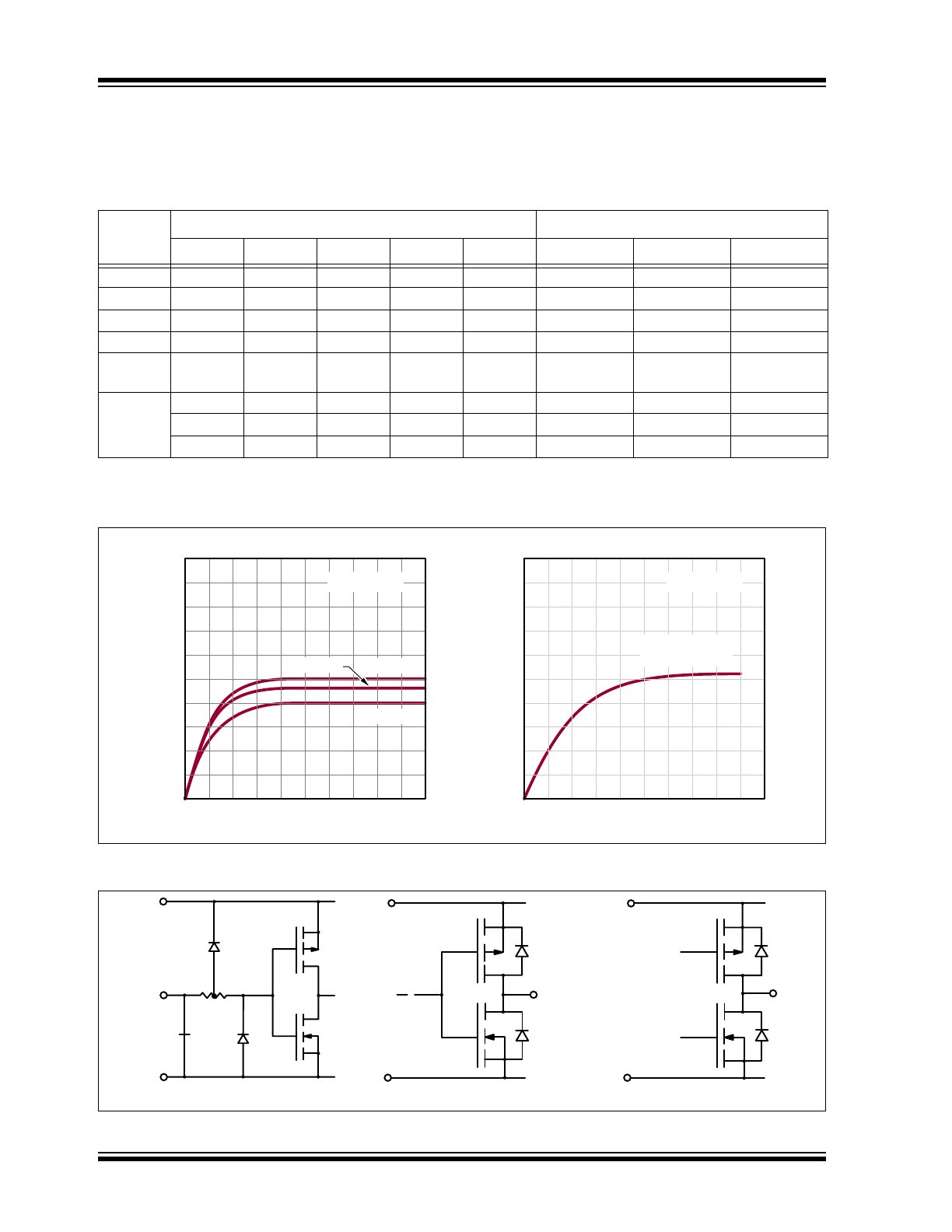
FIGURE 3-1:
HV
OUT
Characteristics
FIGURE 3-2:
Input and Output Equivalent Circuits
TABLE 3-1:
FUNCTIONAL TABLE CLK
I/O
Relations
Inputs
Outputs
CLK
DIR
DATA
POL
OE
Shift Reg
HV
OUT
DATA OUT
O/P HIGH
X
X
H
H
H
*
H
*
O/P OFF
X
X
L
H
H
*
HIGH-Z
*
O/P LOW
X
X
H
L
H
*
L
*
O/P OFF
X
X
L
L
H
*
HIGH-Z
*
O/P OFF
X
X
X
X
L
*
All O/P
HIGH-Z
*
Load S/R,
set DIR
↓
L
X
X
X
Qn→Qn+1
*
Q
34
↓
H
X
X
X
Qn→Qn-1
*
Q
1
No ↓
X
X
X
X
*
No Change
No Change
I (mA)
I (mA)
Volts
0 20 40 60 80 100
180
140
100
60
20
0 20 40 60 80 100
V
PP
> 40V
V
DD
= 12V & 14V
180
140
100
60
20
Volts (V
PP
- HV
OUT
)
Temp = 25
O
C
V
DD
= 12V
Output N-Channel Characteristics through FET Output P-Channel Characteristics through FET
Temp = 25
O
C
V
DD
= 14V
V
DD
= 10V
VDD
DATA
INPUT
GND
VPP
GND
HV
OUT
Logic Inputs
GND
DATA
OUT
Logic Data Output
High Voltage Outputs
VDD
2016 Microchip Technology Inc.
DS20005428A-page 9
HV7022
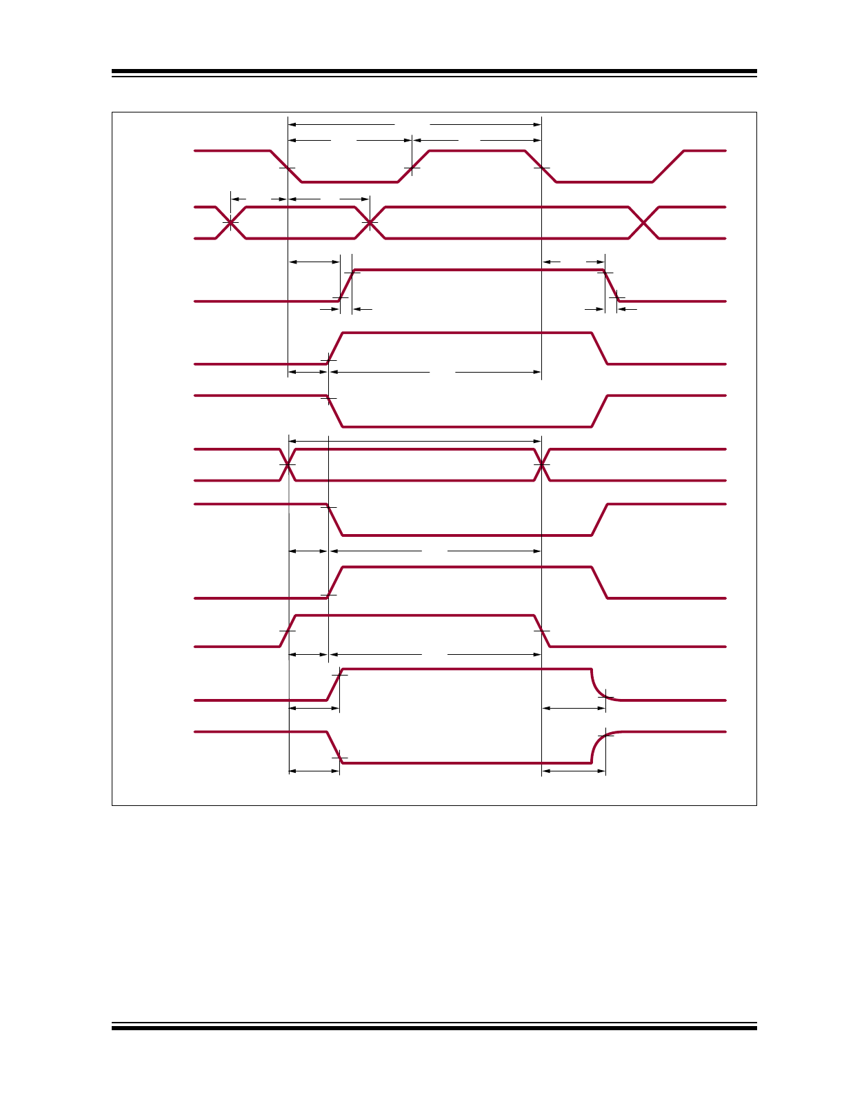
FIGURE 3-3:
Switching Waveforms
50%
50%
DATA OUT
CLK
50%
50%
50%
t
SUD
t
HD
V
IH
t
WL
t
WH
1/f
CLK
t
TLH
90%
10%
t
THL
90%
10%
t
DLH
t
DHL
DATA INPUT
V
IH
V
IL
V
OH
V
OL
t
SUC
10%
90%
t
HC
50%
50%
V
IH
V
IL
90%
POL
10%
t
SUP
SUP
t
HP
50%
50%
t
SUE
t
HE
10%
90%
10%
90%
t
ONL
t
ONH
t
OFFL
t
OFFH
V
IH
V
IL
OE
HV
OUT
HV
OUT
High Impedence
High Impedence
V
IL
V
OH
V
OL
V
OH
V
OL
V
OH
V
OL
V
OH
V
OL
V
OH
V
OL
V
OH
V
OL
HV
OUT
P-CH
HV
OUT
N-CH
HV
OUT
P-CH
HV
OUT
N-CH
HV7022
DS20005428A-page 10
2016 Microchip Technology Inc.
4.0
PACKAGING INFORMATION
4.1
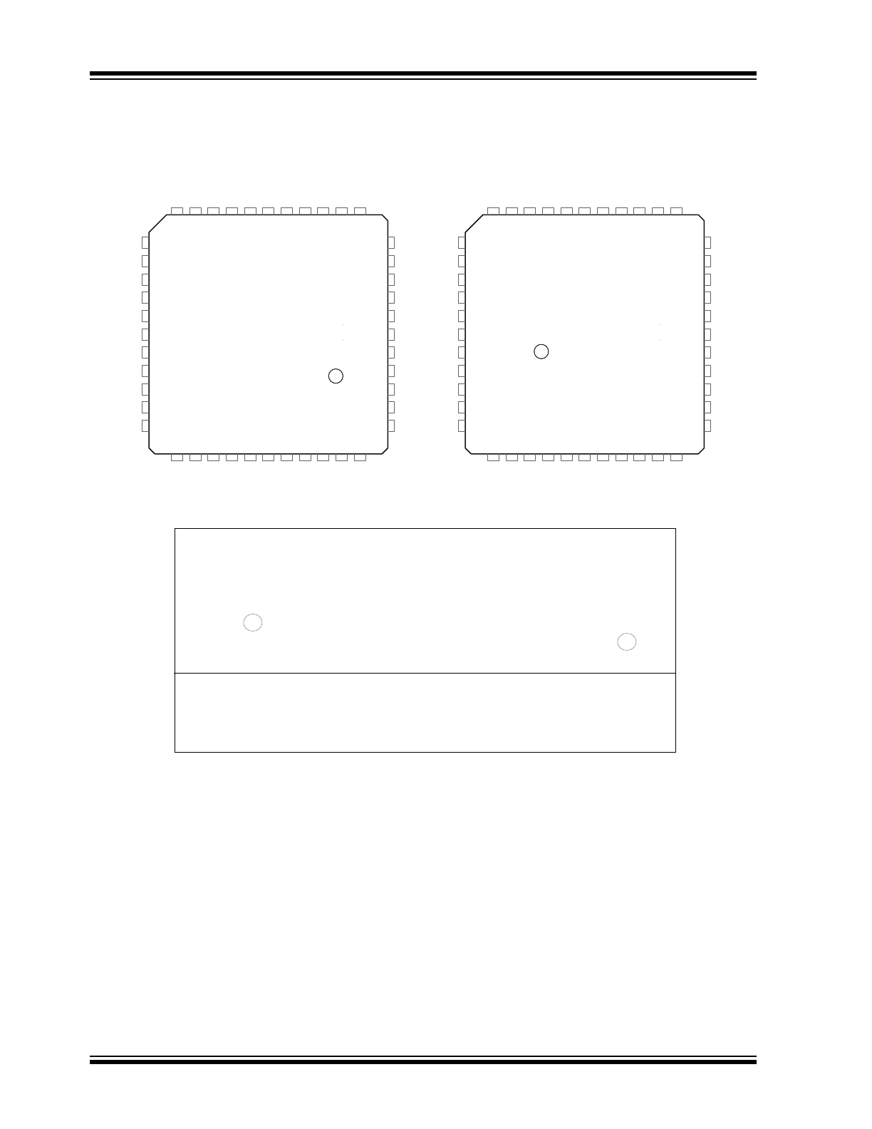
Package Marking Information
Legend: XX...X
Product Code or Customer-specific information
Y
Year code (last digit of calendar year)
YY
Year code (last 2 digits of calendar year)
WW
Week code (week of January 1 is week ‘01’)
NNN
Alphanumeric traceability code
Pb-free JEDEC
®
designator for Matte Tin (Sn)
*
This package is Pb-free. The Pb-free JEDEC designator ( )
can be found on the outer packaging for this package.
Note:
In the event the full Microchip part number cannot be marked on one line, it will
be carried over to the next line, thus limiting the number of available
characters for product code or customer-specific information. Package may or
not include the corporate logo.
3
e
3
e
44-lead PLCC
Example
XXXXXXXXX
XXXXXXXXXXX
YYWWNNN
XXXXXXXXXXX
e3
HV7022PJ-C
1526343
e3