
2015 Microchip Technology Inc.
DS20005425A-page 1
Features
• Processed with High-Voltage CMOS technology
• Low power-level shifting
• Source/sink current minimum 20mA
• Shift register speed 8.0 MHz
• Latched data outputs
• CMOS compatible inputs
• Forward and reverse shifting options
• Diode to V
PP
allows efficient power recovery
Description
HV5308 and HV5408 are low-voltage serial to high-
voltage parallel converters with push-pull outputs.
These devices have been designed for use as a driver
for AC-electroluminescent displays. HV5308 / HV5408
can also be used in any application requiring multiple
output high-voltage, current sourcing, and sinking
capabilities such as driving plasma panels, vacuum flu-
orescent, or large matrix LCD displays.
These devices consist of a 32-bit shift register,
32 latches, and control logic to enable outputs. Data is
shifted through the shift register on the low-to-high tran-
sition of the clock. HV5308 shifts in the clockwise
direction, when viewed from the top of the package,
and HV5408 shifts in the counter-clockwise direction.
A data output buffer is provided for cascading devices.
This output reflects the current status of the last bit of
the shift register (32). Operation of the shift register is
not affected by the LE (latch enable) or the OE (output
enable) inputs. Transfer of data from the shift register
to the latch occurs when the LE input is high. The data
in the latch is retained when LE is low.
HV5308 / HV5408
32-Channel, Serial-to-Parallel Converter
with High-Voltage Push-Pull Outputs
HV5308 / HV5408
DS20005425A-page 2
2015 Microchip Technology Inc.
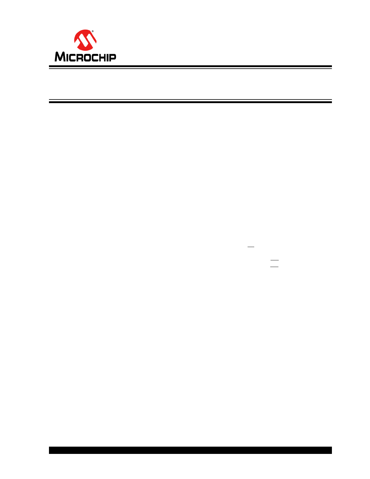
Package Type
Functional Block Diagram
44-Lead PLCC
See
Table 2-1
for pin information
44-Lead PQFP
1
44
1 44
6
40
VPP
LE
OE
HV
OUT
2
•
•
•
28 Additional
Outputs
•
•
•
HV
OUT
31
HV
OUT
1
HV
OUT
32
DATA
INPUT
CLK
DATA
OUT
32 bit
Shift
Register
32 bit
Latches
2015 Microchip Technology Inc.
DS20005425A-page 3
HV5308 / HV5408
Typical Application Circuit
DATA
INPUT
CLK
LE
OE
HV
OUT
1
Micro
Processor
Display
Panel
Columns
Row
Driver
HV
OUT
32
Data Input
for cascading
DATA
OUT
Low Voltage
High Voltage
Shift Register
Latches
Output Contr.
Level
Translators
&
Push-Pull
Output
Buffers
VPP
VDD
HV5308 / HV5408
DS20005425A-page 4
2015 Microchip Technology Inc.
1.0
ELECTRICAL CHARACTERISTICS
ABSOLUTE MAXIMUM RATINGS
†
Supply voltage, V
DD
.................................................................................................................................. -0.5V to +16V
Supply voltage, V
PP
................................................................................................................................... -0.5V to +90V
Logic input levels................................................................................................................................ -0.5V to V
DD
+0.5V
Ground current
1
....................................................................................................................................................... 1.5A
Continuous total power dissipation
2
.................................................................................................................. 1200mW
Operating temperature range.................................................................................................................. -40°C to +85°C
Storage temperature range ................................................................................................................... -65°C to +150°C
1: Duty cycle is limited by the total power dissipated in the package.
2: For operation above 25°C ambient derate linearly to maximum operating temperature at 20mW/°C.
Note 1: L to H = Low to High; H to L = High to Low.
† Notice: Stresses above those listed under “Maximum Ratings” may cause permanent damage to the device. This is
a stress rating only and functional operation of the device at those or any other conditions above those indicated in the
operational listings of this specification is not implied. Exposure to maximum rating conditions for extended periods
may affect device reliability.
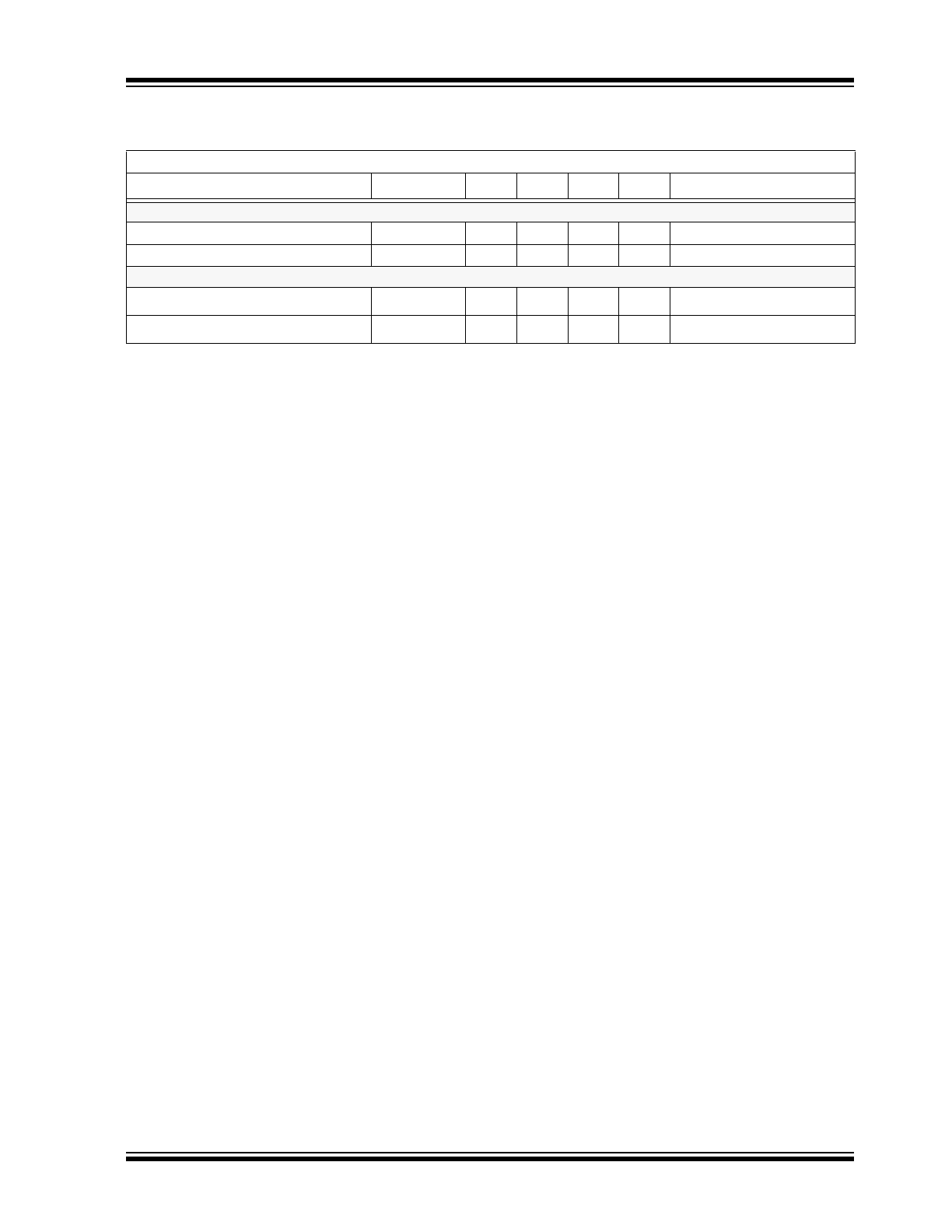
ELECTRICAL CHARACTERISTICS
Electrical Specifications: V
PP
= 60V, V
DD
= 12V, T
A
= 25°C
Parameter
Symbol
Min
Max
Units Conditions
DC Characteristics
V
PP
supply current
I
PP
-
0.5
mA
HV
OUTPUTS
high to low
I
DD
supply current (quiescent)
I
DDQ
-
100
µA
All inputs = V
DD
or GND
I
DD
supply current (operating)
I
DD
-
15
mA
V
DD
= V
DD
max, f
CLK
= 8.0MHz
High level logic input current
I
IH
-
1.0
µA
V
IN
= V
DD
Low level logic input current
I
IL
-
-1.0
µA
V
IN
= 0
High level output voltage
HV
OUT
V
OH
52
-
V
I
OH
= -20mA, -40 to 85°C
I
OH
= -15mA, -55 to 125°C
Data out
10.5
-
V
I
O
= -100µA
Low level output voltage
HV
OUT
V
OL
-
8.0
V
I
OL
= 20mA, -40 to 85°C
I
OL
= 15mA, -55 to 125°C
Data out
-
1.0
V
I
O
= 100µA
HV output clamp diode voltage
V
OC
-
-1.5
V
I
OL
= -100mA
AC Characteristics
Clock frequency
f
CLK
-
8.0
MHz
---
Clock width, High or Low
t
WL
or t
WH
62
-
ns
---
Setup time before CLK rises
t
SU
25
-
ns
---
Hold time after CLK rises
t
H
10
-
ns
---
Data output delay after L to H CLK
t
DLH
(Data)
-
110
ns
C
L
= 15pF, (
Note 1
)
Data output delay after H to L CLK
t
DHL
(Data)
-
110
ns
C
L
= 15pF, (
Note 1
)
LE delay after L to H CLK
t
DLE
50
-
ns
(
Note 1
)
Width of LE pulse
t
WLE
50
-
ns
---
LE setup time before L to H CLK
t
SLE
50
-
ns
(
Note 1
)
Delay from LE to HV
OUT
, L to H
t
ON
-
500
ns
(
Note 1
)
Delay from LE to HV
OUT
, H to L
t
OFF
-
500
ns
(
Note 1
)
2015 Microchip Technology Inc.
DS20005425A-page 5
HV5308 / HV5408
TEMPERATURE SPECIFICATIONS
Electrical Specifications: Unless otherwise specified, for all specifications T
A
=T
J
= +25°C
Parameter
Symbol
Min
Typ
Max
Units Conditions
Temperature Ranges
Operating Temperature
-40
–
85
°C
Storage Temperature
-65
–
150
°C
Package Thermal Resistances
Thermal Resistance, 44-Lead PQFP
θ
ja
–
51
–
°C/W
Thermal Resistance, 44-Lead PLCC
θ
ja
–
37
–
°C/W
HV5308 / HV5408
DS20005425A-page 6
2015 Microchip Technology Inc.
2.0
PIN DESCRIPTION
The locations of the pins are listed in
Package Type
.
TABLE 2-1:
PIN DESCRIPTION PQFP
Pin #
HV5308
HV5408
Description
1
HV
OUT
22
HV
OUT
11
High voltage outputs.
High voltage push-pull outputs, which, depending on controlling
low voltage data, can drive loads either to GND, or to V
PP
rail lev-
els.
2
HV
OUT
21
HV
OUT
12
3
HV
OUT
20
HV
OUT
13
4
HV
OUT
19
HV
OUT
14
5
HV
OUT
18
HV
OUT
15
6
HV
OUT
17
HV
OUT
16
7
HV
OUT
16
HV
OUT
17
8
HV
OUT
15
HV
OUT
18
9
HV
OUT
14
HV
OUT
19
10
HV
OUT
13
HV
OUT
20
11
HV
OUT
12
HV
OUT
21
12
HV
OUT
11
HV
OUT
22
13
HV
OUT
10
HV
OUT
23
14
HV
OUT
9
HV
OUT
24
15
HV
OUT
8
HV
OUT
25
16
HV
OUT
7
HV
OUT
26
17
HV
OUT
6
HV
OUT
27
18
HV
OUT
5
HV
OUT
28
19
HV
OUT
4
HV
OUT
29
20
HV
OUT
3
HV
OUT
30
21
HV
OUT
2
HV
OUT
31
22
HV
OUT
1
HV
OUT
32
23
DATA OUT
DATA OUT
Serial data output.
Data output for cascading to the data input of the next device.
24
N/C
N/C
No connect.
25
26
27
CLK
CLK
Data shift register clock
Input are shifted into the shift register on the positive edge of the
clock.
28
GND
GND
Logic and high voltage ground
29
VPP
VPP
High voltage power rail.
30
VDD
VDD
Low voltage logic power rail.
31
LE
LE
Latch enable input.
When LE is High, shift register data is transferred into a data
latch. When LE is Low, data is latched, and new data can be
clocked into the shift register.
32
DATA IN
DATA IN
Serial data input.
Data needs to be present before each rising edge of the clock.
33
OE
OE
Output enable input.
When OE is Low, all HV outputs are forced into a Low state,
regardless of data in each channel. When OE is High, all HV out-
puts reflect data latched.
34
N/C
N/C
No connect.
2015 Microchip Technology Inc.
DS20005425A-page 7
HV5308 / HV5408
35
HV
OUT
32
HV
OUT
1
High voltage outputs.
High voltage push-pull outputs, which, depending on controlling
low voltage data, can drive loads either to GND, or to V
PP
rail lev-
els.
36
HV
OUT
31
HV
OUT
2
37
HV
OUT
30
HV
OUT
3
38
HV
OUT
29
HV
OUT
4
39
HV
OUT
28
HV
OUT
5
40
HV
OUT
27
HV
OUT
6
41
HV
OUT
26
HV
OUT
7
42
HV
OUT
25
HV
OUT
8
43
HV
OUT
24
HV
OUT
9
44
HV
OUT
23
HV
OUT
10
TABLE 2-1:
PIN DESCRIPTION PQFP (CONTINUED)
Pin #
HV5308
HV5408
Description
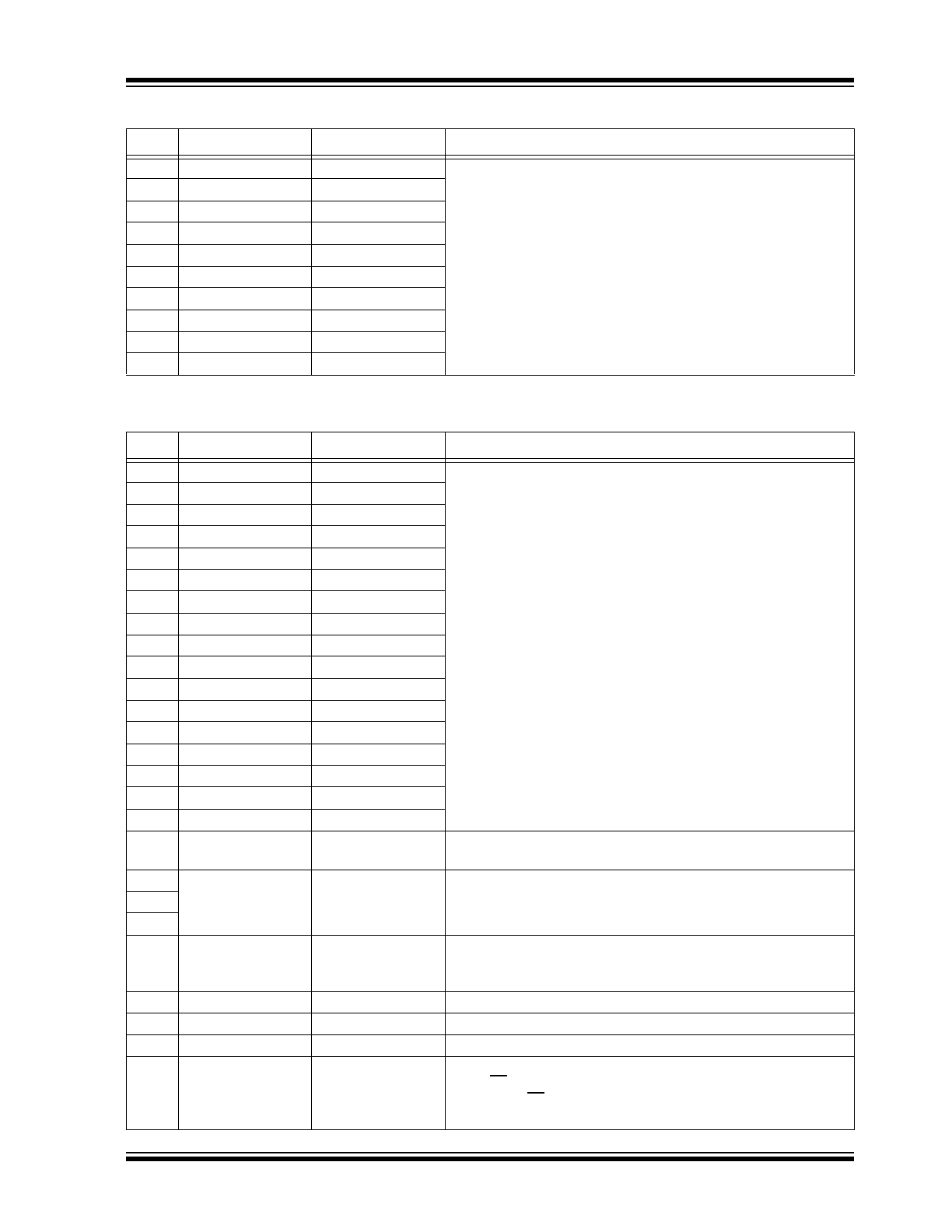
TABLE 2-2:
PIN DESCRIPTION PLCC
Pin #
HV5308
HV5408
Description
1
HV
OUT
17
HV
OUT
16
High voltage outputs.
High voltage push-pull outputs, which, depending on controlling
low voltage data, can drive loads either to GND, or to V
PP
rail lev-
els.
2
HV
OUT
16
HV
OUT
17
3
HV
OUT
15
HV
OUT
18
4
HV
OUT
14
HV
OUT
19
5
HV
OUT
13
HV
OUT
20
6
HV
OUT
12
HV
OUT
21
7
HV
OUT
11
HV
OUT
22
8
HV
OUT
10
HV
OUT
23
9
HV
OUT
9
HV
OUT
24
10
HV
OUT
8
HV
OUT
25
11
HV
OUT
7
HV
OUT
26
12
HV
OUT
6
HV
OUT
27
13
HV
OUT
5
HV
OUT
28
14
HV
OUT
4
HV
OUT
29
15
HV
OUT
3
HV
OUT
30
16
HV
OUT
2
HV
OUT
31
17
HV
OUT
1
HV
OUT
32
18
DATA OUT
DATA OUT
Serial data output.
Data output for cascading to the data input of the next device.
19
N/C
N/C
No connect.
20
21
22
CLK
CLK
Data shift register clock
Input are shifted into the shift register on the positive edge of the
clock.
23
GND
GND
Logic and high voltage ground
24
VPP
VPP
High voltage power rail.
25
VDD
VDD
Low voltage logic power rail.
26
LE
LE
Latch enable input.
When LE is High, shift register data is transferred into a data
latch. When LE is Low, data is latched, and new data can be
clocked into the shift register.
HV5308 / HV5408
DS20005425A-page 8
2015 Microchip Technology Inc.
27
DATA IN
DATA IN
Serial data input.
Data needs to be present before each rising edge of the clock.
28
OE
OE
Output enable input.
When OE is Low, all HV outputs are forced into a LOW state,
regardless of data in each channel. When OE is High, all HV out-
puts reflect data latched.
29
N/C
N/C
No connect.
30
HVOUT32
HV
OUT
1
High voltage outputs.
High voltage push-pull outputs, which, depending on controlling
low voltage data, can drive loads either to GND, or to V
PP
rail lev-
els.
31
HVOUT31
HV
OUT
2
32
HVOUT30
HV
OUT
3
33
HVOUT29
HV
OUT
4
34
HVOUT28
HV
OUT
5
35
HVOUT27
HV
OUT
6
36
HVOUT26
HV
OUT
7
37
HVOUT25
HV
OUT
8
38
HVOUT24
HV
OUT
9
39
HVOUT23
HV
OUT
10
40
HVOUT22
HV
OUT
11
41
HVOUT21
HV
OUT
12
42
HVOUT20
HV
OUT
13
43
HVOUT19
HV
OUT
14
44
HVOUT18
HV
OUT
15
TABLE 2-2:
PIN DESCRIPTION PLCC (CONTINUED)
Pin #
HV5308
HV5408
Description
2015 Microchip Technology Inc.
DS20005425A-page 9
HV5308 / HV5408
3.0
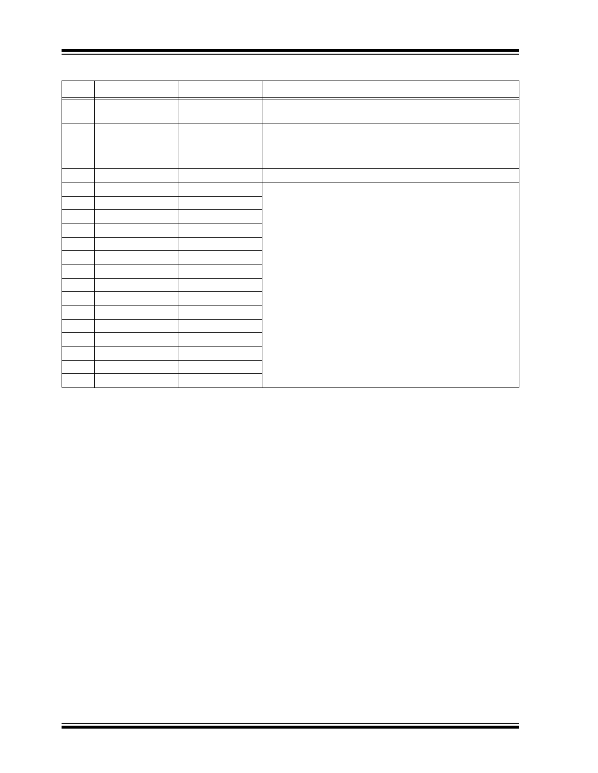
FUNCTIONAL DESCRIPTION
Table 3-1
provides functional information about
HV5308 / HV5408.
Note:
H = High level, L = Low level, ↑ = Low-to-
High transition
Note:
H = High level, L = Low level, X= Don’t Care
3.1
Power-Up and Recommended
Operating Conditions
To power-up HV5308 / HV5408, perform the following
power-up sequence:
1.
Connect ground
2.
Apply V
DD
3.
Set all inputs (Data, CLK, LE, etc.) to a known
state
4.
Apply V
PP
5.
The V
PP
should not fall below V
DD
or float during
operation.
To power-down the device, reverse the steps above.
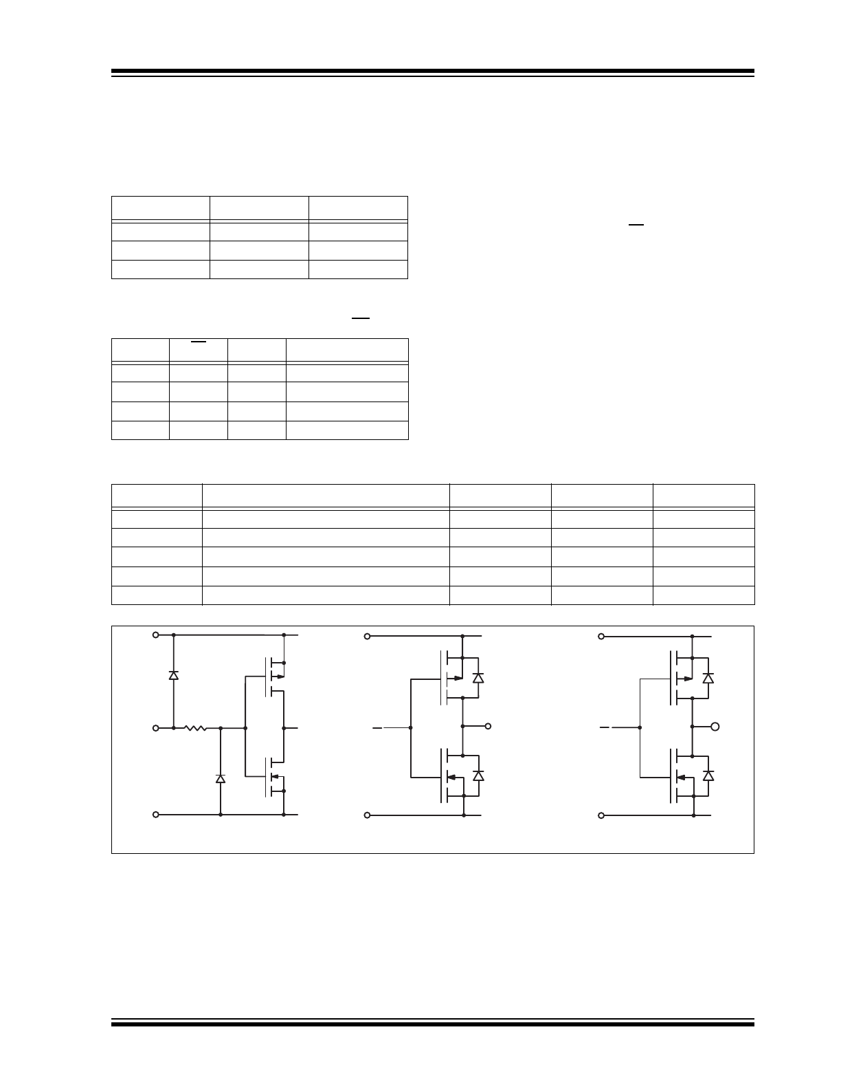
FIGURE 3-1:
Input and Output Equivalent Circuits
TABLE 3-1:
FUNCTIONAL TABLE CLK
DATA IN
CLK
DATA OUT
H
↑
H
L
↑
L
X
No ↑
No change
TABLE 3-2:
FUNCTIONAL TABLE LE, OE
DATA IN
LE
OE
HV
OUT
X
X
L
All HV
OUT
= Low
X
L
H
Previous latched data
H
H
H
H
L
H
H
L
TABLE 3-3:
RECOMMENDED OPERATING CONDITIONS
(-40°C to 85°C)
Symbol
Parameter
Min
Max
Units
V
DD
Logic voltage supply
10.8
13.2
V
V
PP
High voltage supply
8.0
80
V
V
IH
Input high voltage
V
DD
- 2.0
V
DD
V
V
IL
Input low voltage
0
2.0
V
f
CLK
Clock frequency
0
8.0
MHz
VDD
DATA
INPUT
GND
VPP
GND
HV
OUT
Logic Inputs
GND
DATA OUT
Logic Data Output
High Voltage Outputs
VDD
HV5308 / HV5408
DS20005425A-page 10
2015 Microchip Technology Inc.
FIGURE 3-2:
Switching Waveforms
LE
HV
OUT
w/ S/R LOW
Data Valid
50%
DATA
IN
CLK
DATA
OUT
t
SU
t
H
t
WL
t
WH
50%
50%
t
DLH
t
DHL
50%
t
WLE
t
DLE
t
SLE
50%
50%
t
ON
10%
90%
90%
10%
t
OFF
V
IH
V
IL
V
IH
V
IL
V
OH
V
OL
V
OH
V
OL
V
IH
V
IL
V
OH
V
OL
V
OH
V
OL
50%
50%
50%
50%
HV
OUT
w/ S/R HIGH