

2015 Microchip Technology Inc.
DS20005418B-page 1
HV5122 / HV5222
Features
• Processed with High Voltage CMOS technology
• Output voltages to 225V using a ramped supply
voltage
• SINK current minimum 100mA
• Shift register speed 8.0MHz
• Strobe and enable inputs
• CMOS compatible inputs
• Forward and reverse shifting options
Description
HV5122 / HV5222 are low-voltage serial to high-volt-
age parallel converters with open-drain outputs. These
devices are primarily designed for use as a driver for
AC electroluminescent displays. HV5122 / HV5222 can
also be used in any application requiring multiple high-
voltage, current-sinking output capabilities such as
driving inkjet and electrostatic print heads, plasma pan-
els, vacuum fluorescent, or large matrix LCD displays.
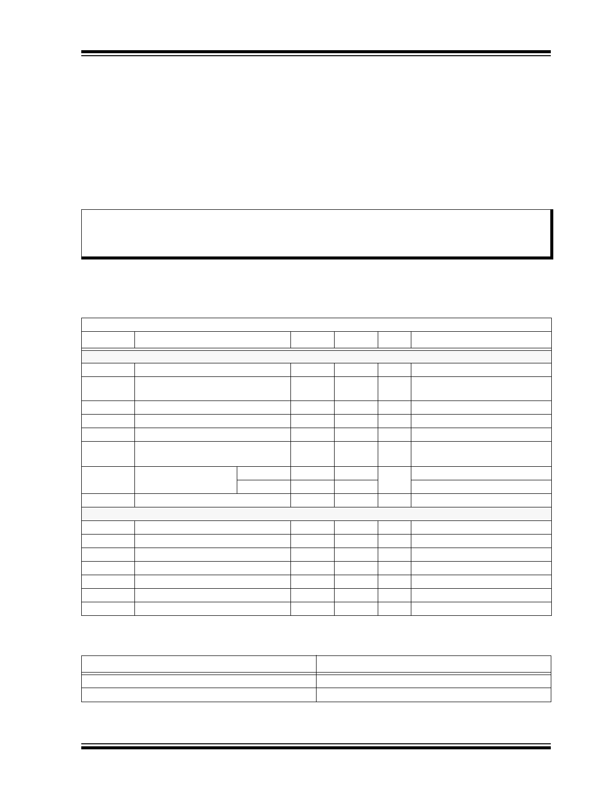
These devices consist of a 32-bit shift register and con-
trol logic to perform the Output Enable and all-on func-
tions. Data is shifted through the shift register on the
high-to-low transition of the clock. HV5122 shifts in the
counter-clockwise direction when viewed from the top
of the package and HV5222 shifts in the clockwise
direction.
For cascading devices, HV5122 / HV5222 provides a
data output buffer that reflects he current status of the
last bit of the shift register. Operation of the shift regis-
ter is not affected by the OE (Output Enable) or the
STR (Strobe) inputs.
HV5122 / HV5222 are designed to be used in systems
which either switch off the high voltage supply before
changing the state of the high voltage outputs or which
limit the current through each output.
32-Channel, Serial-to-Parallel Converter
with Open-Drain Outputs
HV5122 / HV5222
DS20005418B-page 2
2015 Microchip Technology Inc.
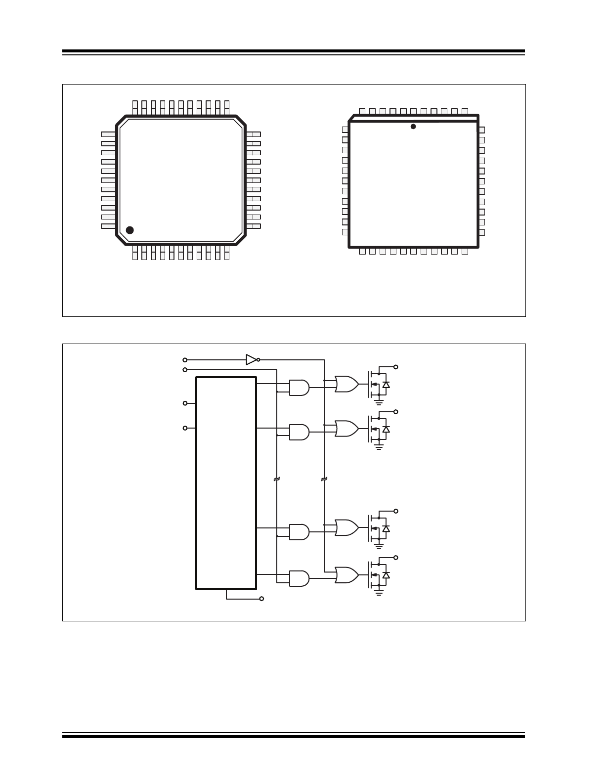
Package Type
Functional Block Diagram
44-Lead PLCC
See
Table 2-1
for pin information
44-Lead PQFP
1
44
1 44
6
40
HV
OUT
2
•
•
•
28 Additional
Outputs
•
•
•
HV
OUT
31
OE
DATA
INPUT
CLK
Data Out
STR
HV
OUT
1
HV
OUT
32
32 bit
Static Shift
Register
2015 Microchip Technology Inc.
DS20005418B-page 3
HV5122 / HV5222
1.0
ELECTRICAL CHARACTERISTICS
ABSOLUTE MAXIMUM RATINGS
†
Supply voltage, V
DD
...................................................................................................................................-0.5V to +15V
Supply voltage, V
PP
.................................................................................................................................-0.5V to +250V
Logic input levels ............................................................................................................................... -0.5V to V
DD
+0.5V
Ground current
1
....................................................................................................................................................... 1.5A
Continuous total power dissipation
2
.................................................................................................................. 1200mW
Operating temperature range.................................................................................................................. -40°C to +85°C
Storage temperature range ................................................................................................................... -65°C to +150°C
1: Duty cycle is limited by the total power dissipated in the package.
2: For operation above 25°C ambient derate linearly to maximum operating temperature at 20mW/°C.
† Notice: Stresses above those listed under “Maximum Ratings” may cause permanent damage to the device. This is
a stress rating only and functional operation of the device at those or any other conditions above those indicated in the
operational listings of this specification is not implied. Exposure to maximum rating conditions for extended periods
may affect device reliability.
TABLE 1-1:
ELECTRICAL CHARACTERISTICS
Electrical Specifications: Over recommended conditions unless otherwise specified
Symbol
Parameter
Min
Max
Units Conditions
DC Characteristics
I
DD
V
DD
supply current
-
15
mA
f
CLK
= 8.0MHz, f
DATA
= 4.0MHz
I
DDQ
Quiescent V
DD
supply current
-
100
µA
D
IN
= 0V, all input logic pins = 0V,
all outputs off
I
O(OFF)
Off-state output current
-
10
µA
All outputs high, all switches parallel
I
IH
High level logic input current
-
1.0
µA
V
IN
= V
DD
I
IL
Low level logic input current
-
-1.0
µA
V
IL
= 0
V
OH
High level output data out
V
DD
-
1.0V
-
V
I
DOUT
= -100µA
V
OL
Low level output voltage
HV
OUT
-
15
V
I
HVOUT
= +100mA
Data out
-
1.0
I
DOUT
= +100µA
V
OC
HV
OUT
clamp voltage
-
-1.5
V
I
OL
= -100mA
AC Characteristics (V
DD
= 12V, T
A
=25°C)
f
CLK
Clock frequency
-
8.0
MHz
t
W
Clock width, high or low
62
-
ns
t
SU
Data setup time before CLK falls
25
-
ns
t
H
Data hold time after CLK falls
10
-
ns
t
ON
Turn-on time, HV
OUT
from strobe
-
500
ns
R
L
= 2.0kΩ to 200V
t
DHL
Data output delay after H to L CLK
-
100
ns
C
L
= 15pF
t
DLH
Data output delay after L to H CLK
-
100
ns
C
L
= 15pF
TABLE 1-2:
TYPICAL THERMAL RESISTANCE
Package
θ
ja
44-Lead PQFP
51°C/W
44-Lead PLCC
37°C/W
HV5122 / HV5222
DS20005418B-page 4
2015 Microchip Technology Inc.
2.0
PIN DESCRIPTION
The locations of the pins are listed in
Package Type
.
TABLE 2-1:
PIN DESCRIPTION PQFP
Pin #
HV5122
HV5222
Description
1
HV
OUT
11
HV
OUT
22
High voltage outputs.
2
HV
OUT
12
HV
OUT
21
3
HV
OUT
13
HV
OUT
20
4
HV
OUT
14
HV
OUT
19
5
HV
OUT
15
HV
OUT
18
6
HV
OUT
16
HV
OUT
17
7
HV
OUT
17
HV
OUT
16
8
HV
OUT
18
HV
OUT
15
9
HV
OUT
19
HV
OUT
14
10
HV
OUT
20
HV
OUT
13
11
HV
OUT
21
HV
OUT
12
12
HV
OUT
22
HV
OUT
11
13
HV
OUT
23
HV
OUT
10
14
HV
OUT
24
HV
OUT
9
15
HV
OUT
25
HV
OUT
8
16
HV
OUT
26
HV
OUT
7
17
HV
OUT
27
HV
OUT
6
18
HV
OUT
28
HV
OUT
5
19
HV
OUT
29
HV
OUT
4
20
HV
OUT
30
HV
OUT
3
21
HV
OUT
31
HV
OUT
2
22
HV
OUT
32
HV
OUT
1
23
DATA OUT
DATA OUT
Data output for cascading to the data input of the next device.
24
N/C
N/C
No connect.
25
26
27
28
OE
OE
Output enable input.
When OE is LOW, all HV outputs are forced into a LOW state,
regardless of data in each channel. When OE is HIGH, all HV
outputs reflect data latched.
29
CLK
CLK
Data shift register clock. Input are shifted into the shift register on
the positive edge of the clock.
30
GND
GND
Logic and high voltage ground.
31
VDD
VDD
Low voltage logic power rail.
32
STR
STR
Strobe.
33
DATA IN
DATA IN
Serial data input. Data needs to be present before each rising
edge of the clock.
34
N/C
N/C
No connect.
2015 Microchip Technology Inc.
DS20005418B-page 5
HV5122 / HV5222
35
HV
OUT
1
HV
OUT
32
High voltage outputs.
36
HV
OUT
2
HV
OUT
31
37
HV
OUT
3
HV
OUT
30
38
HV
OUT
4
HV
OUT
29
39
HV
OUT
5
HV
OUT
28
40
HV
OUT
6
HV
OUT
27
41
HV
OUT
7
HV
OUT
26
42
HV
OUT
8
HV
OUT
25
43
HV
OUT
9
HV
OUT
24
44
HV
OUT
10
HV
OUT
23
TABLE 2-1:
PIN DESCRIPTION PQFP (CONTINUED)
Pin #
HV5122
HV5222
Description
TABLE 2-2:
PIN DESCRIPTION PLCC
Pin #
HV5122
HV5222
Description
1
HV
OUT
16
HV
OUT
17
High voltage outputs
2
HV
OUT
17
HV
OUT
16
3
HV
OUT
18
HV
OUT
15
4
HV
OUT
19
HV
OUT
14
5
HV
OUT
20
HV
OUT
13
6
HV
OUT
21
HV
OUT
12
7
HV
OUT
22
HV
OUT
11
8
HV
OUT
23
HV
OUT
10
9
HV
OUT
24
HV
OUT
9
10
HV
OUT
25
HV
OUT
8
11
HV
OUT
26
HV
OUT
7
12
HV
OUT
27
HV
OUT
6
13
HV
OUT
28
HV
OUT
5
14
HV
OUT
29
HV
OUT
4
15
HV
OUT
30
HV
OUT
3
16
HV
OUT
31
HV
OUT
2
17
HV
OUT
32
HV
OUT
1
18
DATA OUT
DATA OUT
Data output for cascading to the data input of the next device.
19
N/C
N/C
No connect.
20
21
22
23
OE
OE
Output enable input.
When OE is LOW, all HV outputs are forced into a LOW state,
regardless of data in each channel. When OE is HIGH, all HV
outputs reflect data latched.
24
CLK
CLK
Data shift register clock. Input are shifted into the shift register on
the positive edge of the clock.
25
GND
GND
Logic and high voltage ground.
26
VDD
VDD
Low voltage logic power rail.
27
STR
STR
Strobe.
HV5122 / HV5222
DS20005418B-page 6
2015 Microchip Technology Inc.
28
DATA IN
DATA IN
Serial data input. Data needs to be present before each rising
edge of the clock.
29
N/C
N/C
No connect.
30
HV
OUT
1
HV
OUT
32
High voltage outputs.
31
HV
OUT
2
HV
OUT
31
32
HV
OUT
3
HV
OUT
30
33
HV
OUT
4
HV
OUT
29
34
HV
OUT
5
HV
OUT
28
35
HV
OUT
6
HV
OUT
27
36
HV
OUT
7
HV
OUT
26
37
HV
OUT
8
HV
OUT
25
38
HV
OUT
9
HV
OUT
24
39
HV
OUT
10
HV
OUT
23
40
HV
OUT
11
HV
OUT
22
41
HV
OUT
12
HV
OUT
21
42
HV
OUT
13
HV
OUT
20
43
HV
OUT
14
HV
OUT
19
44
HV
OUT
15
HV
OUT
18
TABLE 2-2:
PIN DESCRIPTION PLCC (CONTINUED)
Pin #
HV5122
HV5222
Description
2015 Microchip Technology Inc.
DS20005418B-page 7
HV5122 / HV5222
3.0
FUNCTIONAL DESCRIPTION
Table 3-1
provides functional information about
HV5122 / HV5222.
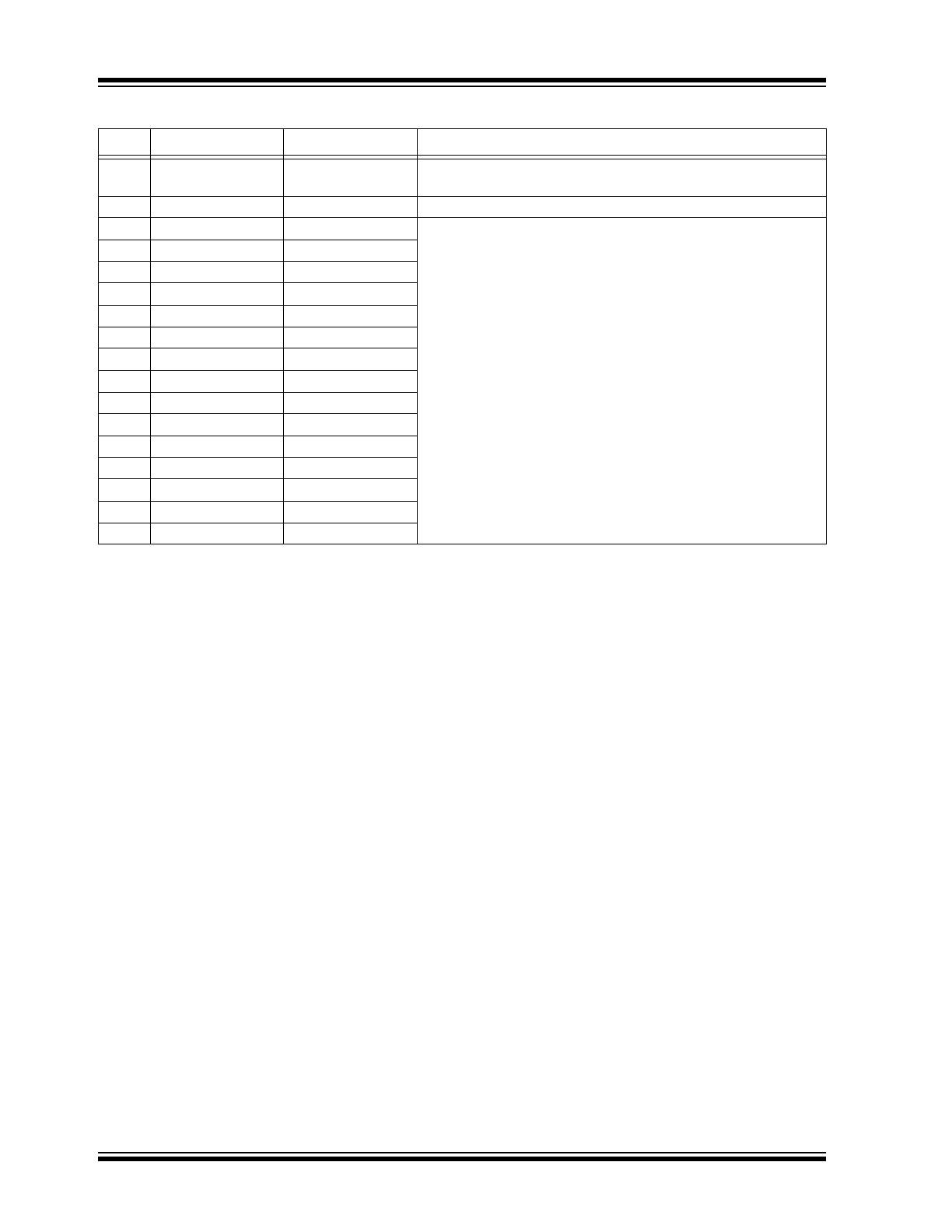
Note 1: H = high level, L = low level, X = irrelevant, ↓ = high-to-low transition
2: ●= dependent on previous stage’s state before the last CLK high-to-low transition
3.1
Power-Up and Recommended
Operating Conditions
To power-up HV5122 / HV5222, perform the following
power-up sequence:
1.
Connect ground
2.
Apply V
DD
3.
Set all inputs to a known state
To power-down the device, reverse the steps above.
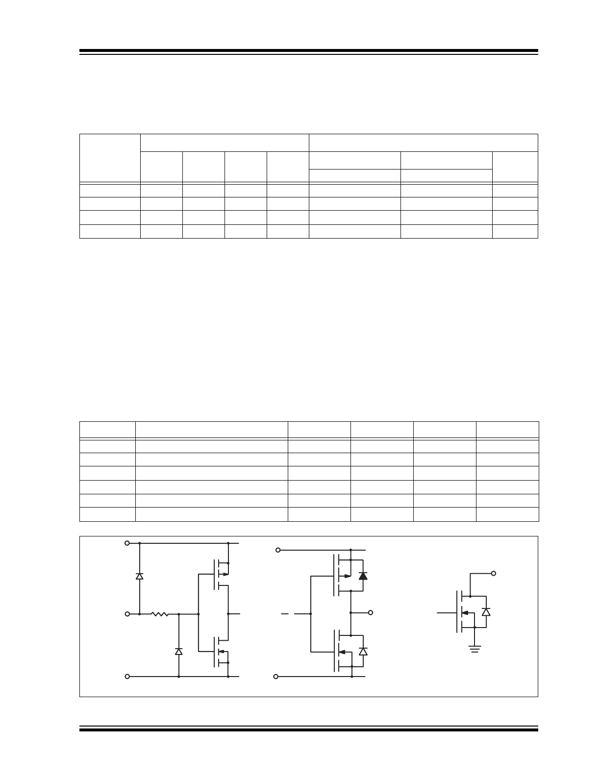
FIGURE 3-1:
Input and Output Equivalent Circuits
TABLE 3-1:
FUNCTIONAL TABLE
Function
Inputs
Outputs
Data In
CLK
OE
STR
Shift Reg
HV Outputs
Data Out
1
2...32
1
2...32
All on
X
X
X
L
●
●...●
ON
ON...ON
●
All off
X
X
L
H
●
●...●
OFF
OFF...OFF
●
Load S/R
H/L
↓
L
H
H/L
Q1...Q31
OFF
OFF...OFF
Q32
Output Enable
X
H/L
H
H
H/L
●...●
ON/OFF
●...●
●
TABLE 3-2:
RECOMMENDED OPERATING CONDITIONS
Symbol
Parameter
Min
Typ
Max
Units
V
DD
Logic voltage supply
10.8
12
13.2
V
HV
OUT
High voltage output
-0.3
-
225
V
V
IH
High-level input voltage
V
DD
-2.0
-
V
DD
V
V
IL
Low-level input voltage
0
-
2.0
V
f
CLK
Clock frequency
-
-
8.0
MHz
T
A
Operating free-air temperature
-40
-
+85
°C
VDD
INPUT
GND
HV
OUT
Logic Inputs
GND
DATA
OUT
Logic Data Output
High Voltage Outputs
VDD
HV
IN
GND
HV5122 / HV5222
DS20005418B-page 8
2015 Microchip Technology Inc.
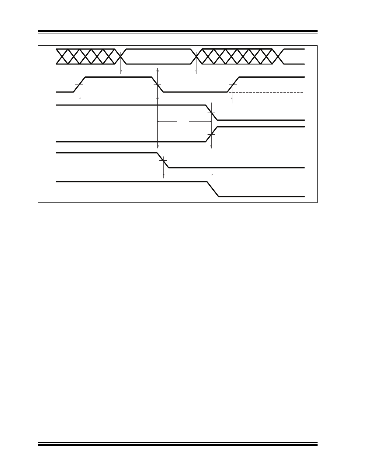
FIGURE 3-2:
Switching Waveforms
DATA
IN
Data Valid 1
CLK
DATA
OUT
DATA
OUT
STR
t
DLH
t
SU
t
H
t
WL
t
WH
t
DHL
HV
OUT
50% 50% 50%
50%
50%
15V
t
ON
12V
0V
12V
0V
2015 Microchip Technology Inc.
DS20005418B-page 9
HV5122 / HV5222
4.0
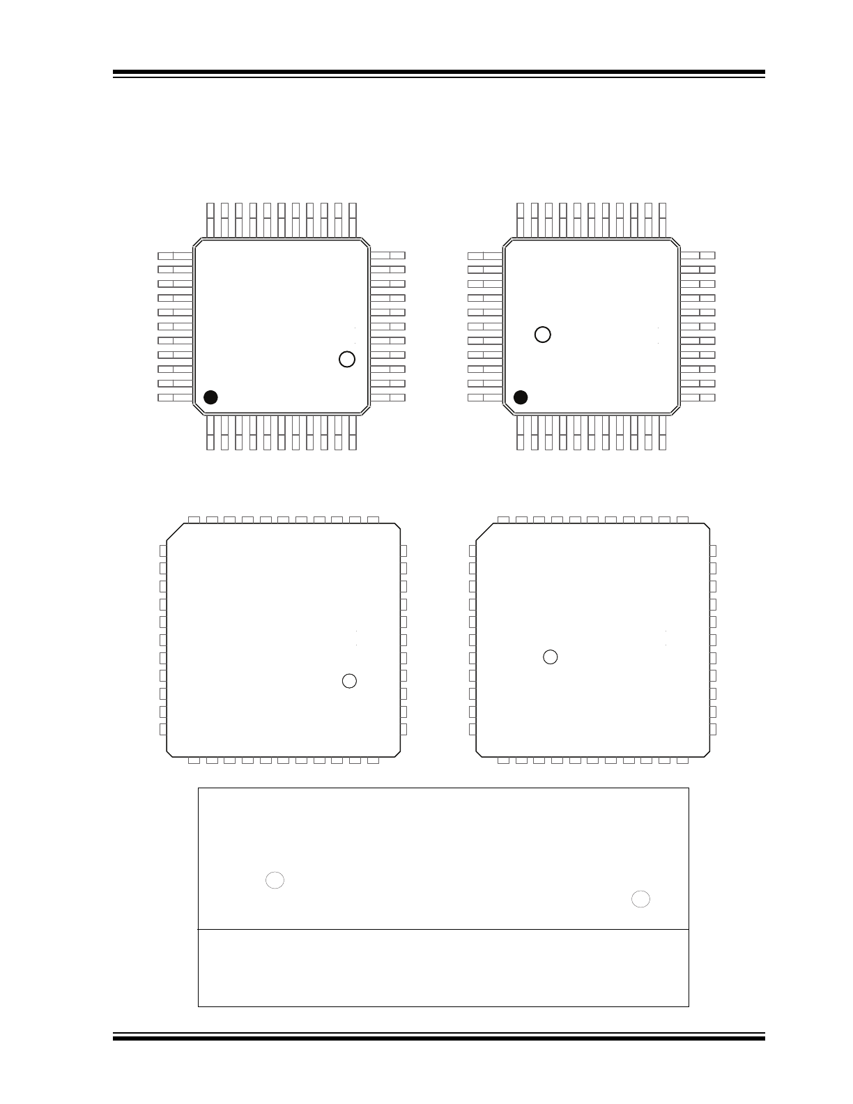
PACKAGING INFORMATION
4.1
Package Marking Information
Legend: XX...X
Product Code or Customer-specific information
Y
Year code (last digit of calendar year)
YY
Year code (last 2 digits of calendar year)
WW
Week code (week of January 1 is week ‘01’)
NNN
Alphanumeric traceability code
Pb-free JEDEC
®
designator for Matte Tin (Sn)
*
This package is Pb-free. The Pb-free JEDEC designator ( )
can be found on the outer packaging for this package.
Note:
In the event the full Microchip part number cannot be marked on one line, it will
be carried over to the next line, thus limiting the number of available
characters for product code or customer-specific information. Package may or
not include the corporate logo.
3
e
3
e
44-lead PLCC
Example
XXXXXXXXX
XXXXXXXXXXX
YYWWNNN
XXXXXXXXXXX
e3
HV5122PJ
1526343
e3
44-lead PQFP
Example
XXXXXXXX
XXXXXXXXXX
XXXXXXXXXX
YYWWNNN
e3
HV5122PG
1526343
e3
HV5122 / HV5222
DS20005418B-page 10
2015 Microchip Technology Inc.
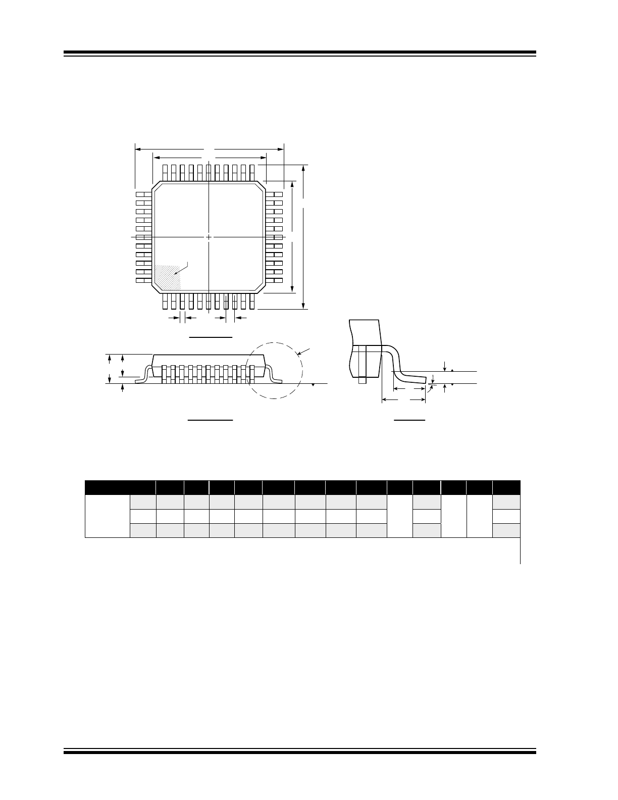
44-Lead PQFP Package Outline (PG)
10.00x10.00mm body, 2.35mm height (max), 0.80mm pitch
Symbol
A
A1
A2
b
D
D1
E
E1
e
L
L1
L2
ș
Dimension
(mm)
MIN
1.95*
0.00
1.95
0.30
13.65*
9.80*
13.65*
9.80*
0.80
BSC
0.73
1.95
REF
0.25
BSC
0
O
NOM
-
-
2.00
-
13.90
10.00
13.90
10.00
0.88
3.5
O
MAX
2.35
0.25
2.10
0.45
14.15*
10.20*
14.15*
10.20*
1.03
7
O
JEDEC Registration MO-112, Variation AA-2, Issue B, Sep.1995.
7KLVGLPHQVLRQLVQRWVSHFL¿HGLQWKH-('(&GUDZLQJ
Drawings not to scale.
S
D
# DSPD 44PQFPPG V
i
C041309
1
44
Seating
Plane
Gauge
Plane
θ
L
L1
L2
View B
View B
Seating
Plane
Top View
D
D1
E
E1
b
e
Side View
A2
A
A1
Note 1
(Index Area
D1/4 x E1/4)
Note:
1.
$3LQLGHQWL¿HUPXVWEHORFDWHGLQWKHLQGH[DUHDLQGLFDWHG7KH3LQLGHQWL¿HUFDQEHDPROGHGPDUNLGHQWL¿HUDQHPEHGGHGPHWDOPDUNHURU
a printed indicator.
Note: For the most current package drawings, see the Microchip Packaging Specification at www.microchip.com/packaging.
Note: For the most current package drawings, see the Microchip Packaging Specification at www.microchip.com/packaging.