

2015 Microchip Technology Inc.
DS20005394A-page 1
LR745
Features
• Accepts inputs from 35 to 450V
• Output current limiting
• For PWM ICs with start-up threshold voltage of
13.9 - 18.0V
• Very low power consumption after start-up
Applications
• Notebook and laptop computers
• Telecommunication power supplies
• Battery chargers
• Motor controllers
Description
LR745 is a high input voltage SMPS start-up circuit.
LR745 is ideally suited for use with industry standard
low-voltage, Pulse-Width Modulation (PWM) ICs hav-
ing start thresholds of 13.9 to 18.0V. It allows the PWM
ICs to be operated from rectified 120 or 240VAC lines,
and eliminates the use of power resistors often used for
this purpose.
The internal circuitry of the LR745 allows the PWM ICs
to operate at a V
CC
voltage below their start-threshold
voltage after start-up. The auxiliary voltage can be less
than the start-threshold voltage, which allows for
improved efficiency. Current from the high voltage line
is drawn only during the start-up period. After start-up,
the internal, high-voltage line is disconnected from the
IC, thereby reducing the continuous power dissipation
to a minimum.
High-Input Voltage SMPS Start-up
LR745
DS20005394A-page 2
2015 Microchip Technology Inc.
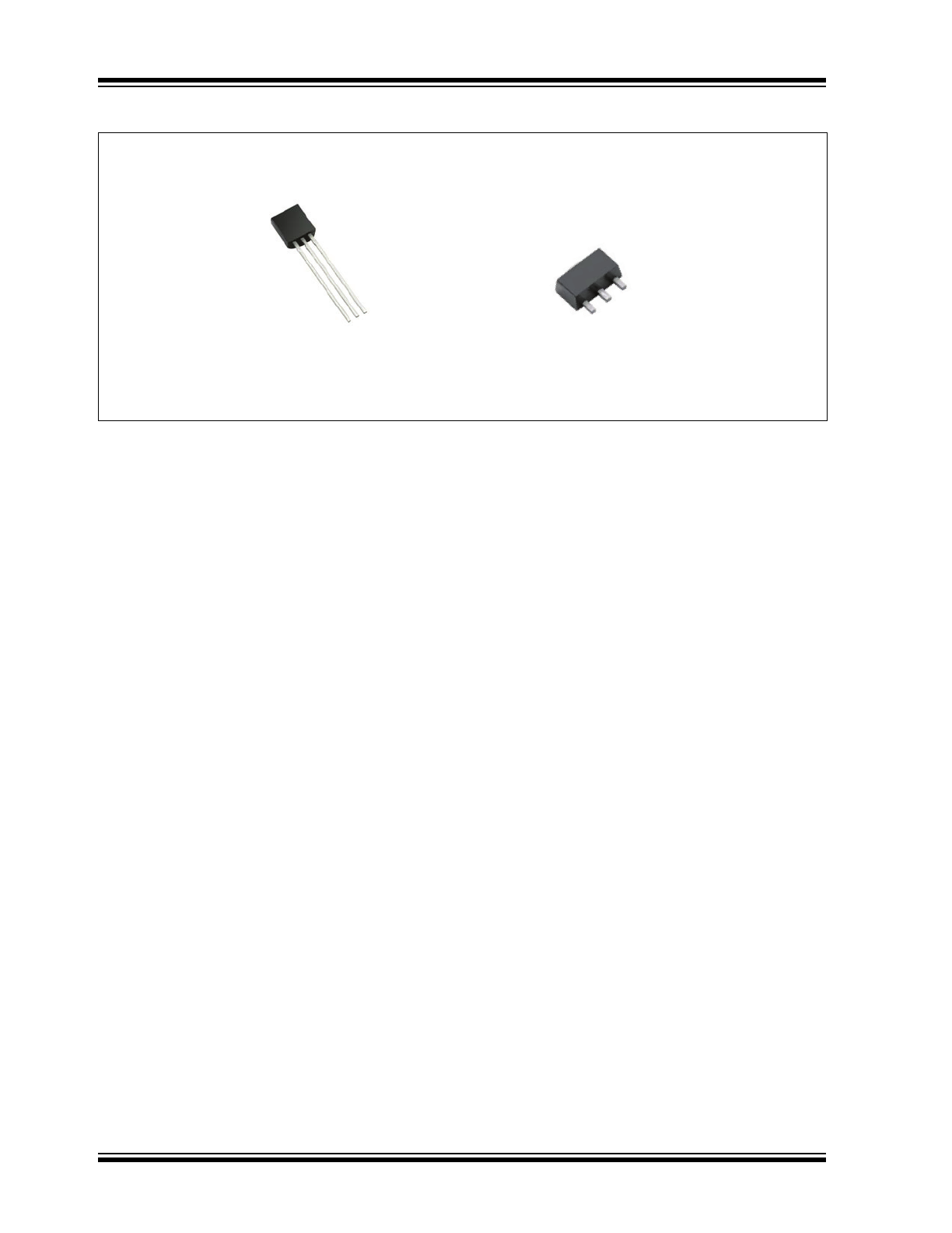
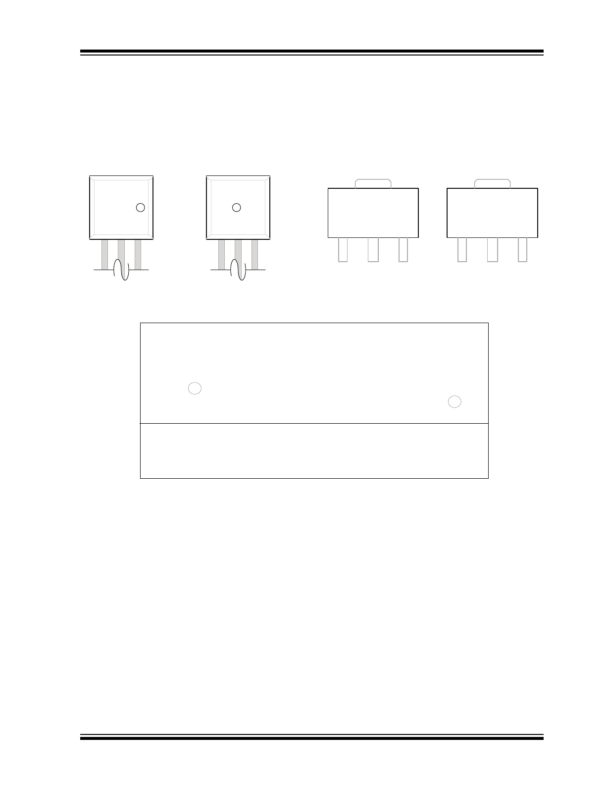
Package Type
TO-92
See
Table 2-1
for pin information
TO-243AA (SOT-89)
VIN
VOUT
GND
GND
GND
VIN
VOUT
2015 Microchip Technology Inc.
DS20005394A-page 3
LR745
1.0
ELECTRICAL CHARACTERISTICS
ABSOLUTE MAXIMUM RATINGS
Input Voltage .................................................................................................................................................................................. 450V
Output voltage.................................................................................................................................................................................. 25V
Operating and storage temperature............................................................................................................................. -55°C to +150°C
Note: Stresses above those listed under “Absolute Maximum Ratings” may cause permanent damage to the device. This is a stress
rating only and functional operation of the device at those or any other conditions, above those indicated in the operational listings of
this specification, is not implied. Exposure to maximum rating conditions for extended periods may affect device reliability.
1.1
ELECTRICAL SPECIFICATIONS
TABLE 1-1:
ELECTRICAL CHARACTERISTICS
1
1
Test Conditions unless otherwise specified: T
A
= 25°C, V
IN
= 450V
Symbol
Parameter
Min
Typ
Max
Units Conditions
V
OUT
Output voltage
18.0
24
V
I
OUT
= 0
V
OUT
over temperature
17.7
24.3
V
I
OUT
= 0, T
A
= -40°C to +85°C
I
OUT
Output current limiting
2.0
3.0
4.0
mA
V
IN
Operating input voltage range
35
450
V
I
INQ
Input quiescent current
500
µA
V
IN
= 400V, I
OUT
= 0
V
OFF
Output turn off voltage
12.6
13.25
13.9
V
V
OFF
over temperature
12.3
13.25
14.2
V
T
A
= -40°C to +85°C
V
RESET
Output reset voltage
6.3
7.0
7.7
V
V
RESET
over temperature
6.0
7.0
8.0
V
T
A
= -40°C to +85°C
I
OFF
V
IN
off-state leakage current
75
µA
V
IN
= 400V
V
AUX
External voltage applied to
V
OUT
22
V
I
AUX
Input current applied to V
OUT
500
µA
V
AUX
= 22V
TABLE 1-2:
THERMAL CHARACTERISTICS
Package
θja
TO-92
132°C/W
TO-243AA (SOT-89)
133°C/W

LR745
DS20005394A-page 4
2015 Microchip Technology Inc.
2.0
PIN DESCRIPTION
The locations of the pins are listed in
Package Type
.
TABLE 2-1:
PIN DESCRIPTION
Function
Description
VIN
Regulator input. 8 - 450V.
GND
Ground return for all internal circuitry. This pin must be electrically connected to circuit common.
VOUT
Regulator output.
2015 Microchip Technology Inc.
DS20005394A-page 5
LR745
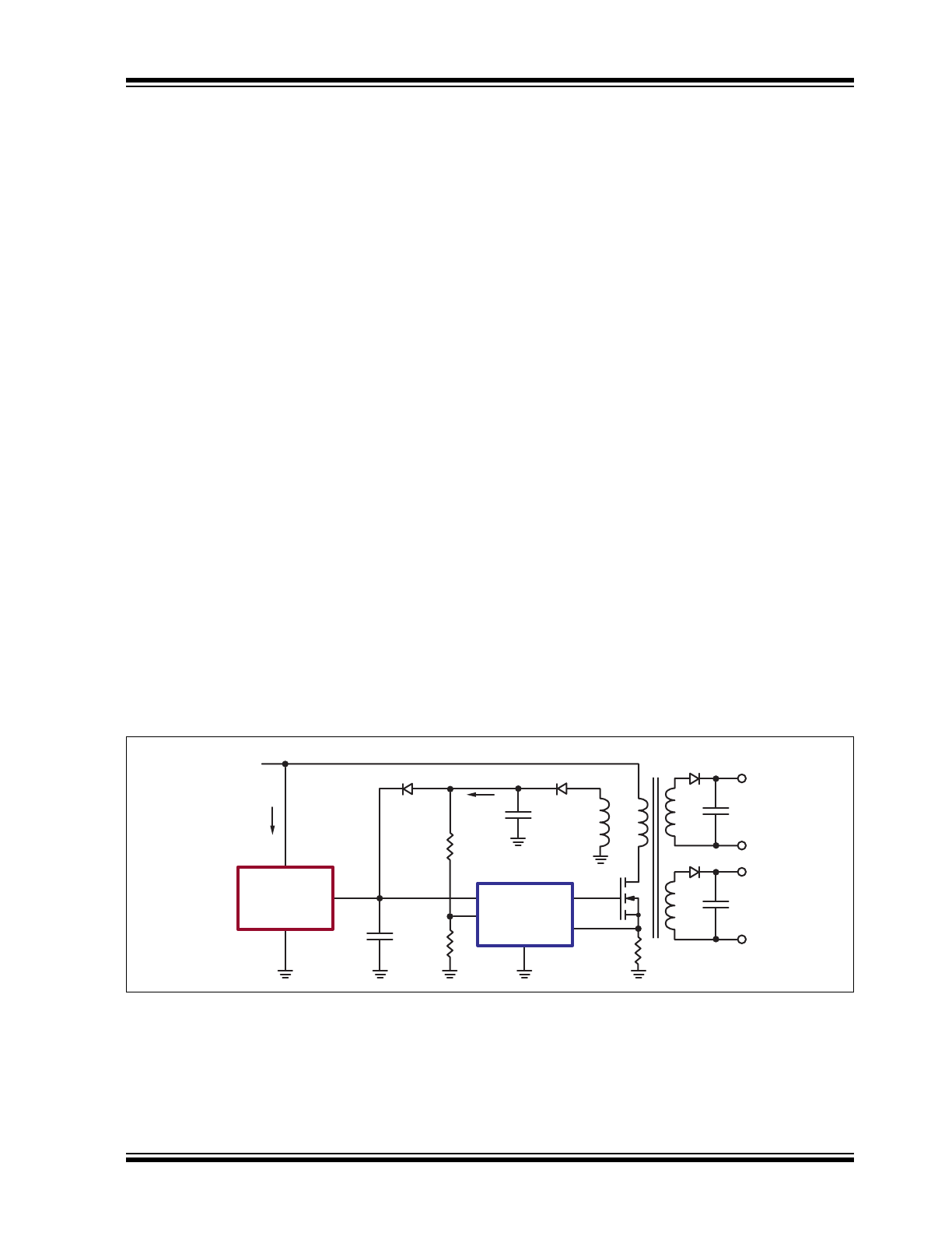
3.0
APPLICATION INFORMATION
Figure 3-1
shows a simplified typical configuration of a
switch mode power supply, SMPS, using LR745 in the
start-up circuit.
LR745’s VOUT terminal is connected to the VCC line of
a PWM IC. An auxiliary winding on the transformer
generates a V
CC
voltage to power the PWM IC after
start-up. LR745 supplies power for the PWM IC only
during start-up. After start-up, LR745 turns off and the
auxiliary winding supplies power for the PWM IC.
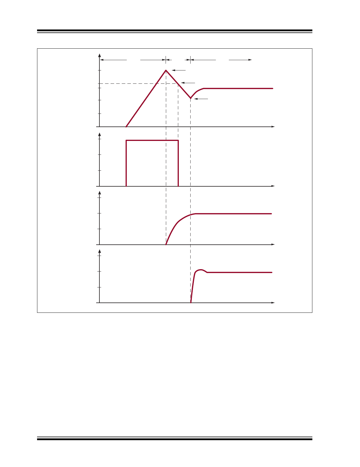
Figure 3-2
shows the typical current and voltage wave-
forms at various stages from power-up to operation
powered by the auxiliary winding.
3.1
Stage I
Once a voltage is applied on VIN, LR745 starts to
charge the V
CC
capacitor, C
1
. The V
CC
voltage starts to
increase at a rate limited by the internal current limiter
of 3.0mA. The PWM IC is in its start-up condition and
will typically draw 0.5mA from the V
CC
line. The V
CC
voltage will continue to increase until it reaches the
PWM IC’s start threshold voltage, typically 16V.
3.2
Stage II
Once V
CC
reaches 16V, the PWM IC is in its operating
condition and will typically draw 20mA, depending on
the operating frequency and size of the switching
metal–oxide–semiconductor field-effect transistor
(MOSFET). The output of LR745, V
OUT
, is internally
current limited to 3.0mA. The remaining 17mA will be
supplied by C
1
, causing the V
CC
voltage decrease.
When V
CC
decreases to 13.25V, LR745 will turn off its
output, thereby reducing its input current from 3.0mA to
10s of microamperes. At this point, all 20mA will be
supplied by C
1
. The PWM IC can now operate to a min-
imum V
CC
voltage, typically 10V.
Once the switching MOSFET starts operating, the
energy in the primary winding is transferred to the sec-
ondary outputs and the auxiliary winding, thereby build-
ing up V
AUX
. It is necessary to size the V
CC
storage
capacitor, C
1
, such that V
AUX
increases to a voltage
greater than 10V before V
CC
decreases to 10V. This
allows V
AUX
to supply the required operating current for
the PWM IC.
If for some reason the auxiliary voltage does not reach
10V, V
CC
will continue to decrease. Once V
CC
goes
below 10V, the PWM IC will return to its start-up condi-
tion. The PWM IC will now only draw 0.5mA. V
CC
will
continue to decrease but at a much slower rate. Once
V
CC
decreases below 7.0V, LR745 will turn the output,
V
OUT
, back on. V
OUT
will start charging C
1
as described
in Stage I.
3.3
Stage III
At this stage, LR745 output is turned off and the PWM
IC is operating from the V
AUX
supply. The auxiliary volt-
age, V
AUX
, can be designed to vary anywhere between
the minimum operating V
CC
voltage of the PWM IC
(10V) to the maximum auxiliary voltage rating of the
LR745 (22V).
FIGURE 3-1:
SIMPLIFIED SMPS USING LR745
High Voltage
V
IN
VOUT
V
CC
I
AUX
V
AUX
C
1
C
2
D
2
I
IN
GND
LR7
PWM IC
LR745
DS20005394A-page 6
2015 Microchip Technology Inc.
FIGURE 3-2:
START-UP WAVEFORMS
12.0
8.0
4.0
0.0
30.0
20.0
10.0
0.0
PWM IC Start Threshold Voltage
LR7 V
OFF
Trip Point
Auxiliary Supply Powers PWM IC
t
t
t
t
16.0
13.5
12.0
8.0
4.0
0.0
V
OUT
(V)
I
IN
(mA)
V
AUX
(V)
I
AUX
(mA)
V
AUX
= 12V
I
AUX
= 20mA
I
IN
≈ 0mA
3.0
2.0
1.0
0.0
Stage
I
Stage
II
Stage
III
2015 Microchip Technology Inc.
DS20005394A-page 7
LR745
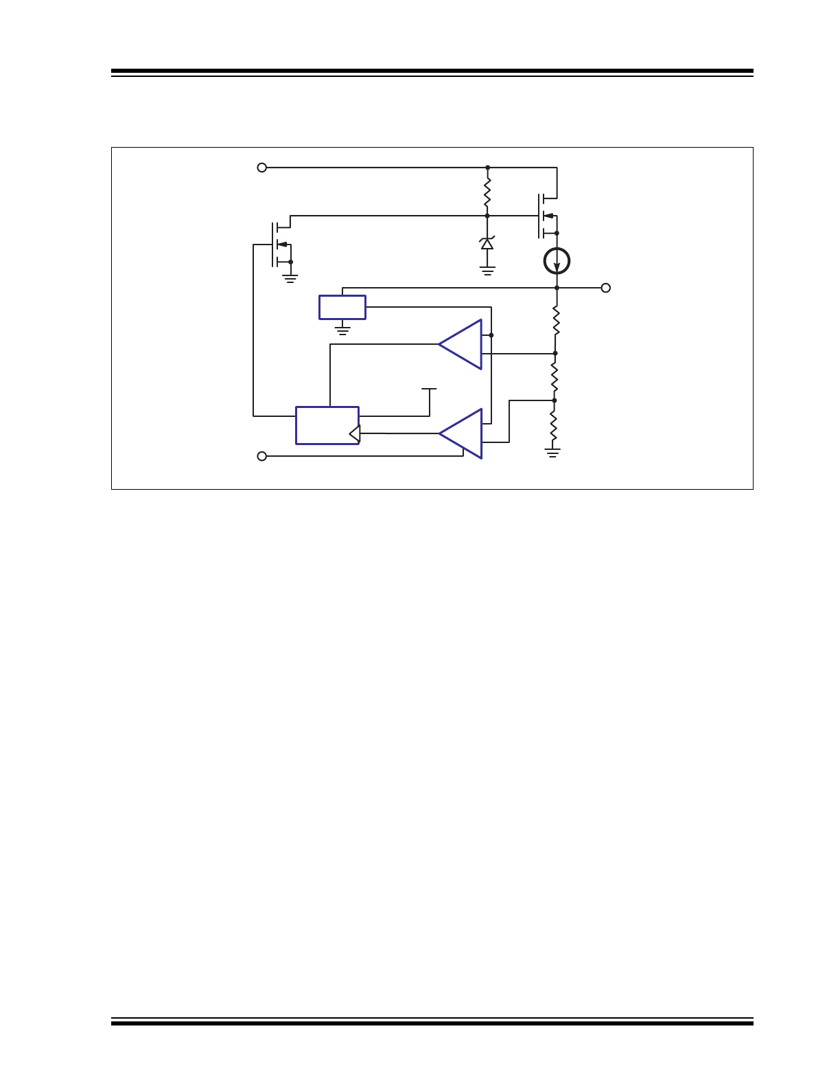
3.4
Block Diagram
FIGURE 3-3:
BLOCK DIAGRAM
LR745 is a high voltage, switch-mode power supply
start-up circuit which has 3 terminals: VIN, GND, and
VOUT. An input voltage range of 35 - 450V DC can be
applied directly at the input VIN pin. The output voltage,
V
OUT
, is monitored by the 2 comparators: comp1 and
comp2. An internal reference, V
REF
, and resistor
divider R1, R2, and R3set the nominal V
OUT
trip points
of 7.0V for comp1 and 13.25V for comp2.
When a voltage is applied on VIN, V
OUT
will start to
ramp up from 0V. When V
OUT
is less than 7.0V, the out-
put of comp1 will be at a logic high state, keeping the D
flip-flop in a reset state. The output of the D flip-flop, Q,
will be at logic low keeping transistor M
2
off. The data
input for the D flip-flop, D, is internally connected to a
logic high. As V
OUT
becomes greater than 7.0V, comp1
will change to a logic low state. V
OUT
will continue to
increase, and the constant current source, typically
3.0mA output, will charge an external storage capaci-
tor. As V
OUT
reaches above 13.25V, the output of
comp2 will then switch from a logic high to a logic low
state. The D flip-flop’s output does not change state
since its clock input is designed to trigger only on a ris-
ing edge, logic low to logic high transition. When there
is no load connected to the output, the output voltage
will continue to increase until it reaches 21.5V, which is
the Zener voltage minus the threshold voltage of tran-
sistor M
1
. The Zener voltage is typically 23V, and the
threshold voltage of M
1
is typically 1.5V. The Zener
diode is biased by resistor R
4
.
V
OUT
will start to decrease when it is connected to an
external load greater than the internal constant current
source, which is the case when the PWM IC starts up.
When V
OUT
falls below 13.25V, the output of comp2 will
switch from a logic low to a logic high. The output of
comp2 will clock in a logic 1 into the D flip-flop, causing
the D flip-flop’s output, Q, to switch from a logic low to
a logic high. Transistor M
2
will then be turned on pulling
the gate of transistor M
1
to ground, thereby turning
transistor M
1
off. Transistor M
1
will remain off as long
as VOUT is greater than 7.0V. Once V
OUT
decreases
below 7.0V, comp1 will reset the D flip-flop, thereby
turning transistor M
2
off and transistor M
1
back on.
CLK
Clock
Q
GND
R D
V
OUT
VOUT
VIN
M2
M
1
R
3
2.0 - 4.0mA
+
23V
-
V
Z
V
REF
Reset
-
comp1
+
-
comp1
+
R
2
R
1
R
4
LR745
DS20005394A-page 8
2015 Microchip Technology Inc.
4.0
DESIGN CONSIDERATIONS
To ensure the best design using LR745, evaluate the
value of C
1
and the SMPS requirements.
4.1
Calculating the value for C
1
Sizing the V
CC
capacitor, C
1
, is an important factor.
Making C
1
too large will cause the SMPS to power up
too slowly. However, if too small, C
1
will not allow the
SMPS to power up due to insufficient charge in the
capacitor to power the IC and MOSFET until the auxil-
iary supply is available. The value of C
1
can be approx-
imated by the following equation:
Definitions:
- f = switching frequency
- N = number of clock cycles required to
charge V
AUX
to V
MIN
value
- I = PWM operating current
- V
START
= PWM IC start threshold rating
- V
MIN
= PWM IC minimum V
CC
operating volt-
age
Consider for example, a PWM IC with a switching fre-
quency of 100KHz, operating current of 20mA, start
threshold of 16V, and a minimum operating voltage of
10V. If 100 clock cycles are required to charge the aux-
iliary voltage to 10V, the minimum value of C
1
is calcu-
lated as follows:
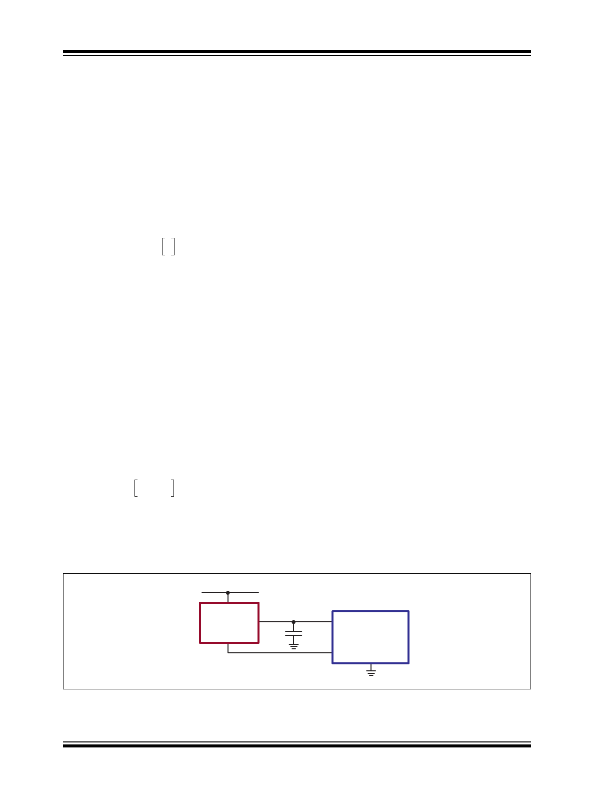
4.2
SMPS with wide minimum to
maximum load
An important point is that the LR745’s output voltage,
V
OUT
, must discharge to below the nominal V
OFF
trip
point of 13.25V in order for its output to turn off. If the
SMPS requires a wide minimum to maximum output
load variation, it will be difficult to guarantee that V
CC
will fall below 13.25V under minimum load conditions.
Consider an SMPS that is required to power small as
well as large loads and is also required to power up
quickly. Such a SMPS may power up too fast with a
small load, not allowing the V
CC
voltage to fall below
13.25V. For such conditions, the circuit in
Figure 4-1
is
recommended.
In
Figure 4-1
, the V
REF
pin of the UC3844 is used to
bias the ground pin of the LR745. The V
REF
pin on the
UC3844 is a 5.0V reference, which stays at 0V until the
V
CC
voltage reaches the start threshold voltage. Once
V
CC
reaches the start threshold voltage, V
REF
will
switch digitally from 0V to 5.0V. During start-up, the
LR745 will be on, and V
CC
will start to increase up to
16V. Once V
CC
reaches16V, the UC3844 will start to
operate and V
REF
will increase from 0V to 5.0V. The
LR745 will see an effective V
OUT
voltage of 11V (16V
minus 5.0V) because the ground of the LR745 is now
at 5.0V. The LR745 will immediately turn off its output,
VOUT, without having to wait for the V
CC
voltage to
decrease. The V
REF
switching from 0 to 5.0V during
start is a common feature in most PWM ICs.
FIGURE 4-1:
USING V
REF
FOR GROUND VOLTAGE
C
1
1
f
---
N 1
V
START
V
MIN
–
------------------------------------
=
C
1
1
100kHz
---------------------
100 20mA
16V 10V
–
-----------------------------------------------------------------
=
C
1
3.3
F
=
GND
VIN
VOUT
VCC
VREF
C
1
PWM IC
LR7
2015 Microchip Technology Inc.
DS20005394A-page 9
LR745
5.0
PACKAGING INFORMATION
5.1
Package Marking Information
Legend: XX...X
Product Code or Customer-specific information
Y
Year code (last digit of calendar year)
YY
Year code (last 2 digits of calendar year)
WW
Week code (week of January 1 is week ‘01’)
NNN
Alphanumeric traceability code
Pb-free JEDEC
®
designator for Matte Tin (Sn)
*
This package is Pb-free. The Pb-free JEDEC designator ( )
can be found on the outer packaging for this package.
Note:
In the event the full Microchip part number cannot be marked on one line, it will
be carried over to the next line, thus limiting the number of available
characters for product code or customer-specific information. Package may or
not include the corporate logo.
3
e
3
e
3-lead TO-243AA *
(SOT-89)
Example
XXXYYWW
NNN
LR7513
343
3-lead TO-92
YWWNNN
XXXXXX
XXXX
e3
Example
513343
LR745
N3
e3
LR745
DS20005394A-page 10
2015 Microchip Technology Inc.
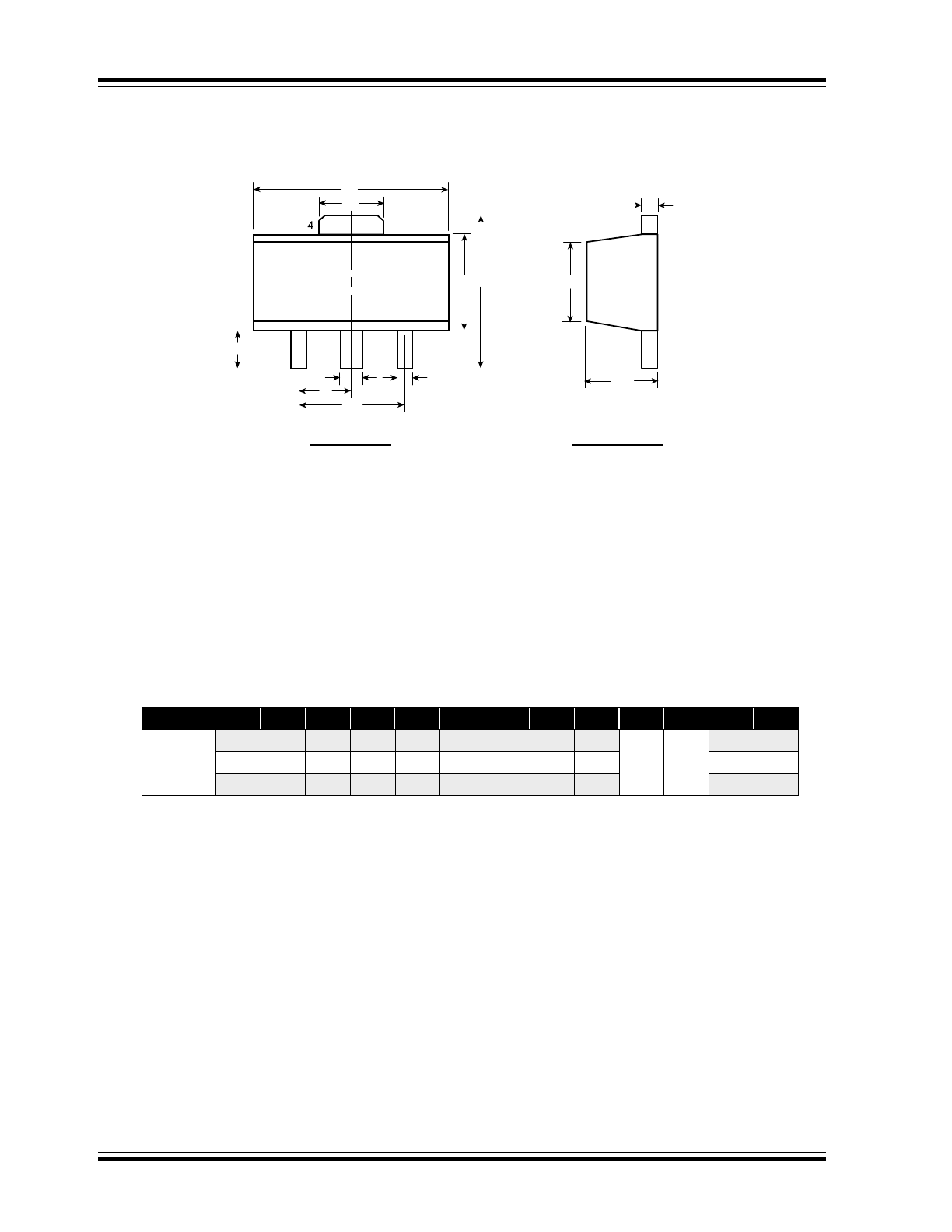
3-Lead TO-243AA (SOT-89) Package Outline (N8)
Symbol
A
b
b1
C
D
D1
E
E1
e
e1
H
L
Dimensions
(mm)
MIN
1.40
0.44
0.36
0.35
4.40
1.62
2.29
2.00
†
1.50
BSC
3.00
BSC
3.94
0.73
†
NOM
-
-
-
-
-
-
-
-
-
-
MAX
1.60
0.56
0.48
0.44
4.60
1.83
2.60
2.29
4.25
1.20
JEDEC Registration TO-243, Variation AA, Issue C, July 1986.
† This dimension differs from the JEDEC drawing
Drawings not to scale.
b
b1
D
D1
E H
E1
C
A
1
2
3
e
e1
Top View
Side View
L
Note: For the most current package drawings, see the Microchip Packaging Specification at www.microchip.com/packaging.
Note: For the most current package drawings, see the Microchip Packaging Specification at www.microchip.com/packaging.