
2015 Microchip Technology Inc.
DS20005384A-page 1
LR645
Features
• Accepts inputs from 15 to 450V
• Output currents: up to 3.0mA continuous, 30mA
peak
• Supply current typically 50µA
• Line regulation typically 0.1mV/V
• Output can be trimmed from 8.0 to 12V
• Output current can be increased to 150mA with
external FET
Applications
• Off-line SMPS startup circuits (pulse loads)
• Low power off-line regulators
• Regulators for noisy inputs
Description
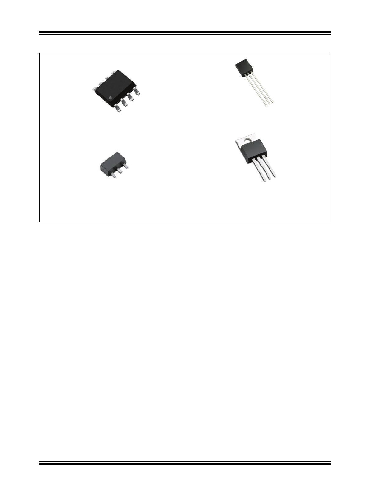
LR645 is a high-input voltage, low-output current, linear
regulator that is available in two versions. A 3-terminal,
fixed-output voltage version is available in TO-92, TO-
220 and SOT-89 packages, as well as an adjustable
voltage version available in an 8-lead SOIC package.
The 3-terminal version of LR645 functions like any
other low-voltage, 3-terminal regulator except it allows
the use of much higher-input voltages. When used in a
Switched-mode Power Supply (SMPS), start-up circuit,
LR645 eliminates the need for large power resistors. In
this application, current is drawn from the high voltage
line only during start-up. Only leakage current flows
after start-up, thereby reducing the continuous power
dissipation to a few milliwatts.
The adjustable-voltage version allows trimming of the
output voltage from 8.0 to 12V. This version can also be
connected to an external depletion mode metal–oxide–
semiconductor field-effect transistor (MOSFET) for
increased output current. When used in conjunction
with depletion mode MOSFET DN2540N5, an output
current of up to 150mA is achieved.
WARNING
The LR645 does NOT provide galvanic isolation. When operated from an AC line, potentially lethal voltages can be
present on the IC. Adequate means of protecting the end user from such voltages must be provided by the circuit
developer.
High-Input Voltage SMPS, Start-up/Linear Regulator
LR645
DS20005384A-page 2
2015 Microchip Technology Inc.
Package Type
8-Lead SOIC
TO-92
See
Table 2-1
for pin information
TO-220
TO-243AA (SOT-89)
VIN
VOUT
GND
GND
+VIN
VOUT
GND
GND
GND
VIN
VOUT
+VIN
VOUT
NC
GND
NC
TRIM
GATE
NC
2015 Microchip Technology Inc.
DS20005384A-page 3
LR645
1.0
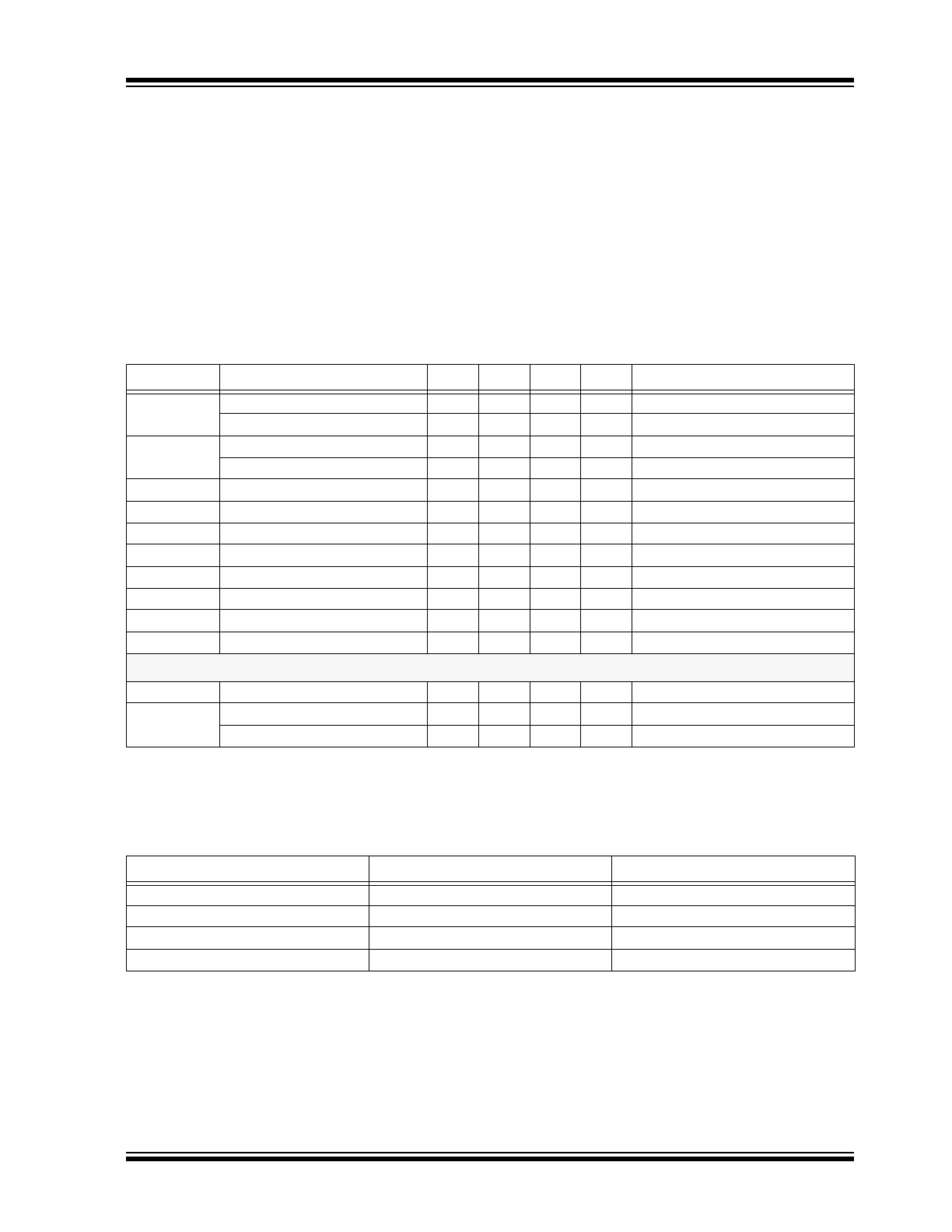
ELECTRICAL CHARACTERISTICS
ABSOLUTE MAXIMUM RATINGS
Input Voltage .................................................................................................................................................................................. 450V
Output voltage............................................................................................................................................................................... 15.5V
Operating and storage temperature............................................................................................................................. -55°C to +150°C
Note: Stresses above those listed under “Absolute Maximum Ratings” may cause permanent damage to the device. This is a stress
rating only and functional operation of the device at those or any other conditions, above those indicated in the operational listings of
this specification, is not implied. Exposure to maximum rating conditions for extended periods may affect device reliability.
1.1
ELECTRICAL SPECIFICATIONS
TABLE 1-1:
ELECTRICAL CHARACTERISTICS
1
1
Test Conditions unless otherwise specified: T
A
= 25°C, V
IN
= 15V-450V, C
OUT
= 0.01
µF
Symbol
Parameter
Min
Typ
Max
Units Conditions
V
OUT
Output voltage
9.3
10
10.7
V
No load
Output voltage over temperature
2
2
Guaranteed by design
9.0
10
11.5
V
T
J
= - 40 to +125°C, No load
∆V
OUT
Line regulation
-
40
200
mV
V
IN
= 15 to 400V, No load
Load regulation
-
150
400
mV
V
IN
= 50V, I
OUT
= 0 to 3.0mA
V
IN
Operating input voltage range
15
-
450
V
I
INQ
Input quiescent current
-
50
150
µA
No Load
I
OFF
VIN off-state leakage current
-
0.1
10
µA
V
AUX
≥ V
OUT
+1V applied to V
OUT
pin
I
AUX
Input current to V
OUT
-
-
200
µA
V
AUX
≥ V
OUT
+1V applied to V
OUT
pin
∆V
OUT
/∆V
IN
Ripple rejection ratio
2
50
60
-
dB
120 Hz, No Load
e
n
Noise voltage
2
-
25
-
µV
0.01 to 100 KHz
I
PEAK
Output peak current
3
3
Pulse test duration <1.0 msec, duty cycle <2%
-
30
-
mA
C
OUT
= 10 µF, V
IN
= 400V
V
AUX
External voltage applied to V
OUT
-
-
13.2
V
8-lead, adjustable voltage version only
V
OUT
Output regulation trim range
2
8
-
12
V
No load
∆V
OUT
Load regulation at 8V trim
2
-
200
400
mV
V
IN
= 15V, I
OUT
= 0 to 1.0 mA
Load regulation at 12V trim
2
-
100
400
mV
V
IN
= 50V, I
OUT
= 0 to 3.0 mA
TABLE 1-2:
THERMAL CHARACTERISTICS
1
Package
θja
Power Dissipation @T
A
=25°C
8-lead SOIC
101°C/W
0.31
TO-92
132°C/W
0.74
TO-220
29°C/W
1.8
TO-243AA (SOT-89)
133°C/W
1.6
1
Mounted on FR5 board; 25mm x 25mm x 1.57mm. Significant P
D
increase possible on ceramic substrate.
LR645
DS20005384A-page 4
2015 Microchip Technology Inc.
2.0
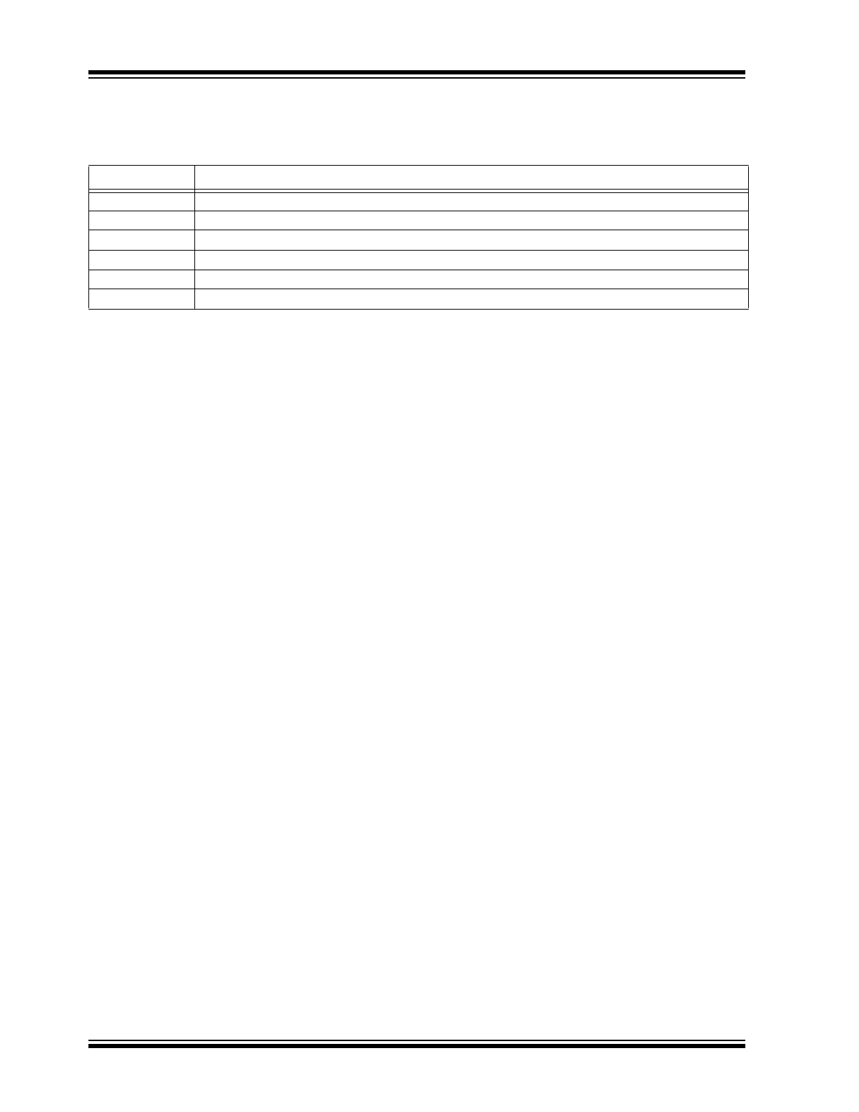
PIN DESCRIPTION
The locations of the pins are listed in
Package Type
.
TABLE 2-1:
PIN DESCRIPTION
Function
Description
VIN
Regulator input. 8 - 450V.
GND
Ground return for all internal circuitry. This pin must be electrically connected to circuit common.
GATE
Output GATE driver for an external N-channel depletion.
TRIM
A voltage divider from V
OUT
to this pin adjusts the output voltage.
VOUT
Regulator output.
NC
No connection.
2015 Microchip Technology Inc.
DS20005384A-page 5
LR645
3.0
FUNCTIONAL DESCRIPTION
3.1
SMPS Start-Up Circuit
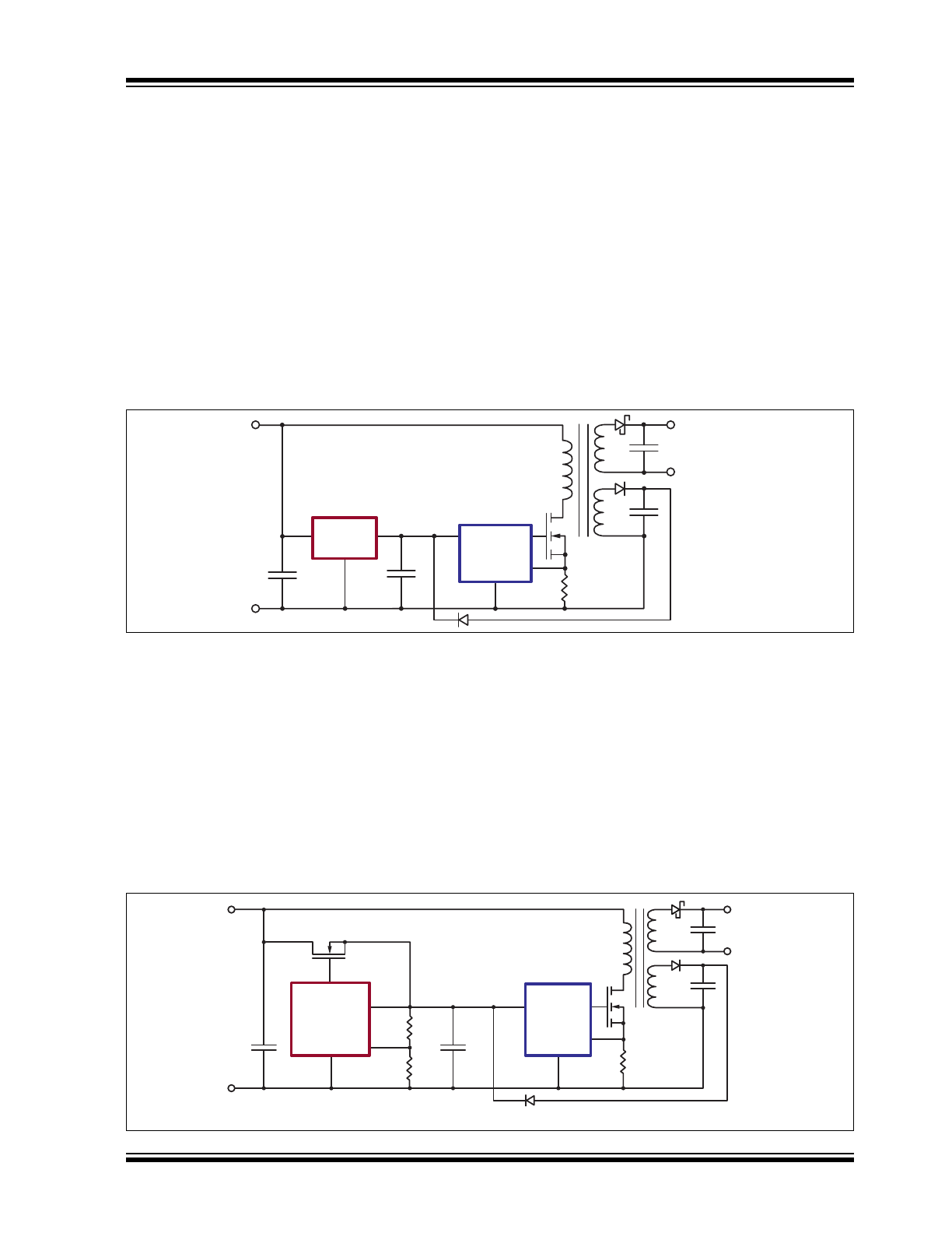
One of the main applications for LR645 is a start-up cir-
cuit for off-line, switch-mode power supplies (SMPS),
as shown in
Figure 3-1
. A minimum output capacitance
of 10 nF is recommended for stability. The wide operat-
ing, input voltage range of LR645 allows the SMPS to
operate and start-up from rectified AC, or a DC voltage
of 15 to 450V, without adjustment.
During start-up, the LR645 powers the V
CC
line of the
Pulse-Width Modulation (PWM) IC with a nominal out-
put voltage of 10V. The auxiliary voltage connected
through a diode to the V
OUT
pin of LR645 will start to
increase. When the auxiliary voltage becomes larger
than the output voltage LR645 turns OFF both its inter-
nal high voltage input line and output voltage, allowing
the auxiliary voltage to power the V
CC
line of the PWM
IC. After startup, LR645 doesn’t draw any input current
from the high-voltage line other than the leakage cur-
rent of the internal MOSFET switch, which is typically
0.1µA.
The 3-terminal version shown in
Figure 3-1
has load
regulation guaranteed from 0 to 3.0mA at a fixed nom-
inal output voltage of 10V. Applications requiring higher
output current and/or a different output voltage can use
the 8 pin adjustable version.
FIGURE 3-1:
SMPS START-UP CIRCUIT
3.2
High-Current SMPS Start-Up
Circuit
The 8-lead version of LR645 has connections for an
external depletion-mode MOSFET for higher-output
current and external resistors for adjustable-output
voltage. As shown in
Figure 3-2
, the output current is
increased to 150mA by using the DN2540, a 400V
depletion-mode MOSFET. The maximum operating
input voltage will be limited by the drain-to-source,
breakdown voltage of the external MOSFET, but can-
not exceed the 450V rating of LR645.
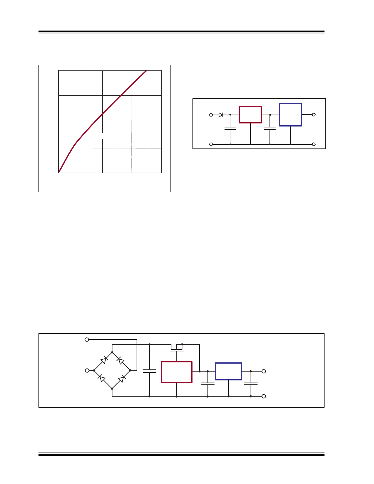
The output voltage can be adjusted from 8 to 12V with
two external resistors: R1 and R2. The ratio of R2/R1
determines the output voltage. R2 is connected
between the V
OUT
and TRIM pins; R1 is connected
between TRIM and GND pins.
Figure 3-3
is a curve
showing output voltage versus resistor ratio R2/R1.
The optimum range for R1 + R2 is 200KΩ to 300KΩ.
This minimizes loading and optimizes accuracy of the
output voltage.
Figure 3-3
uses an R1 + R2 of 250KΩ.
FIGURE 3-2:
HIGH-CURRENT SMPS START-UP CIRCUIT
+
15 - 450V
-
+
5.0V
-
V
AUX
= 12V
C
OUT
C
IN
VCC
PWM IC
LR6
GND
VIN
R2
R1
+
15V
to
400V
–
+
5.0V
–
DN2540
C
OUT
C
IN
VCC
V
AUX
= 12V
Note:
When used with the DN25, +V
IN
is not connected on the LR6.
PWM IC
LR645
VOUT
GND
GATE
TRIM
LR645
DS20005384A-page 6
2015 Microchip Technology Inc.
FIGURE 3-3:
TYPICAL OUTPUT
VOLTAGE VS RESISTOR
RATIO
3.3
Off Line Linear Regulator
Circuits that require low voltages to operate logic and
analog circuits benefit from LR645. The conventional
use of step-down transformers can be eliminated,
thereby saving space and cost. Some examples of low-
voltage applications are: proximity controlled light
switches, street lamp controls, and low-voltage power
supplies for appliances such as washing machines,
dishwashers, and refrigerators.
The wide operating-input voltage range of 15 to 450V,
as well as the ripple rejection ratio of 50dB minimum,
allows the use of a small, high-voltage input capacitor.
The input AC line can be either full-wave or half-wave
rectified. A minimum output capacitance of 0.01µF is
recommended for output stability.
Figure 3-4
shows the LR645 as a pre-regulator to a
precision regulator for high precision regulation. Higher
output current is also possible by using an external
depletion-mode MOSFET DN2540N5 as shown in
Figure 3-5
.
FIGURE 3-4:
CASCADING FOR
PRECISION
3.4
Power Dissipation Considerations
LR645 is a true linear regulator. Its power dissipation is
therefore a function of input voltage and output load
current. For example, if the LR645 provides a continu-
ous load current of 3mA at 10V, while its input voltage
is 400V, total dissipation in the LR645 will be:
The 1.23 watts is for continuous operation. This is
within the dissipation capabilities of the TO-220 and
SOT-89 packages. See
Table 1-2
on Page 3 for derat-
ings. For SMPS start-up applications, the output cur-
rent is usually required only during start-up. This
duration depends upon the auxiliary supply output
capacitor and C
OUT
, but is typically a few hundred mil-
liseconds. All package types of the LR645 have been
characterized for use with a C
OUT
of at least 10µF, and
an AC line of 277V.
FIGURE 3-5:
HIGH-CURRENT REGULATION
12
10
8
2.5 3.0 3.5 4.0
Resistor Ratio (R2/R1)
Output Voltage (V)
R1 + R2 = 250kΩ
5.000V
± 0.002V
@
0 to 3mA
AC Line
24V - 277V
C
OUT
0.1μF
C
IN
1.0μF
LR6
Max
875
ACSA
P
DISS
V
IN
V
OUT
–
I
OUT
I
MAXQuiescent
+
400V 10V
–
3.0mA 150
A
+
1.23Watts
=
=
=
AC Line
24 - 277V
5.0V
+
0 - 150mA
-
5.0V
REG
C
OUT
C
IN
V
OUT
GATE
DN2540N5
GND
LR645
2015 Microchip Technology Inc.
DS20005384A-page 7
LR645
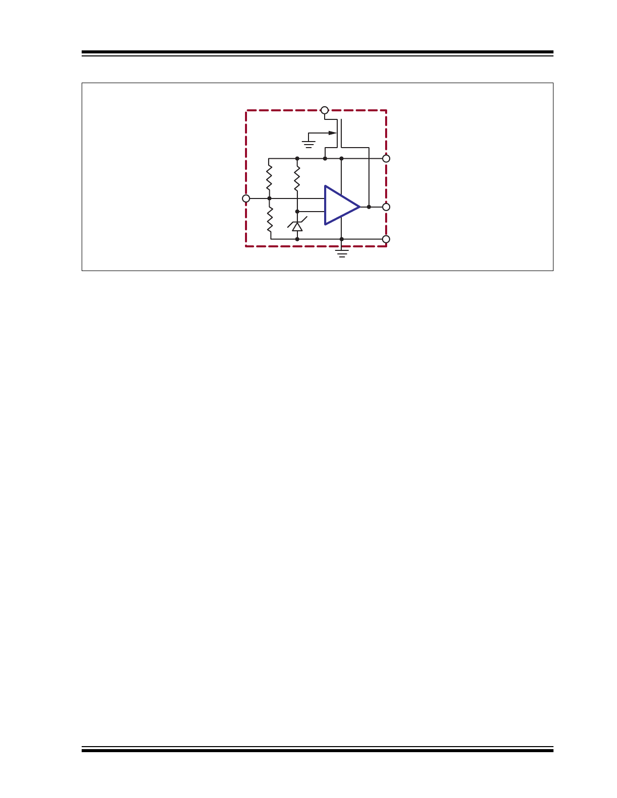
FIGURE 3-6:
BLOCK DIAGRAM
VOUT
GND
GATE
VIN
TRIM
+
–
LR645
LR645
DS20005384A-page 8
2015 Microchip Technology Inc.
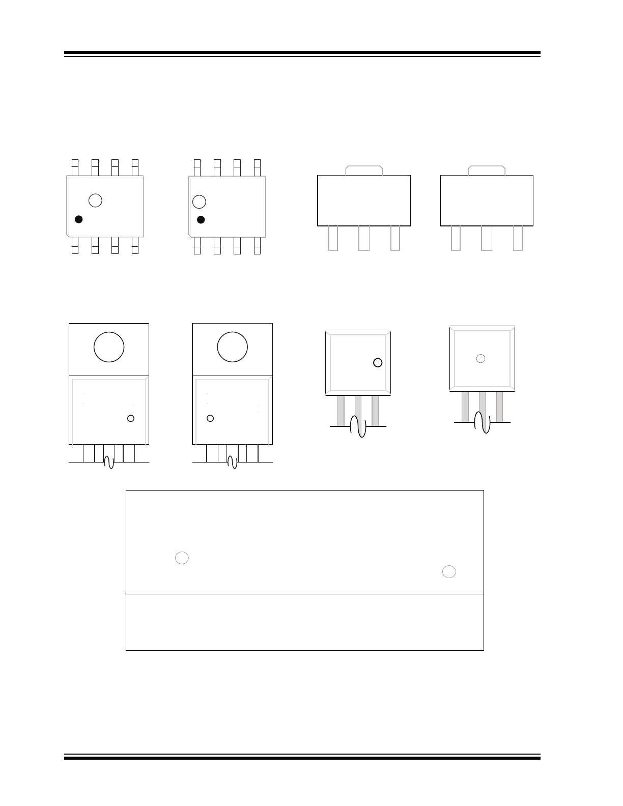
4.0
PACKAGING INFORMATION
4.1
Package Marking Information
Legend: XX...X
Product Code or Customer-specific information
Y
Year code (last digit of calendar year)
YY
Year code (last 2 digits of calendar year)
WW
Week code (week of January 1 is week ‘01’)
NNN
Alphanumeric traceability code
Pb-free JEDEC
®
designator for Matte Tin (Sn)
*
This package is Pb-free. The Pb-free JEDEC designator ( )
can be found on the outer packaging for this package.
Note:
In the event the full Microchip part number cannot be marked on one line, it will
be carried over to the next line, thus limiting the number of available
characters for product code or customer-specific information. Package may or
not include the corporate logo.
3
e
3
e
8-lead SOIC
Example
NNN
XX
XXXXXXXX
YYWW
e3
343
LR645LG
1508
e3
3-lead TO-243AA *
(SOT-89)
Example
XXXYYWW
NNN
LR6508
343
3-lead TO-220
Example
YYWWNNN
XXXXXXX
XXXXXXXXX
e3
1508343
LR645N5
e3
3-lead TO-92
YWWNNN
XXXXXX
XXXX
e3
Example
508343
LR645
N3
e3
2015 Microchip Technology Inc.
DS20005384A-page 9
LR645
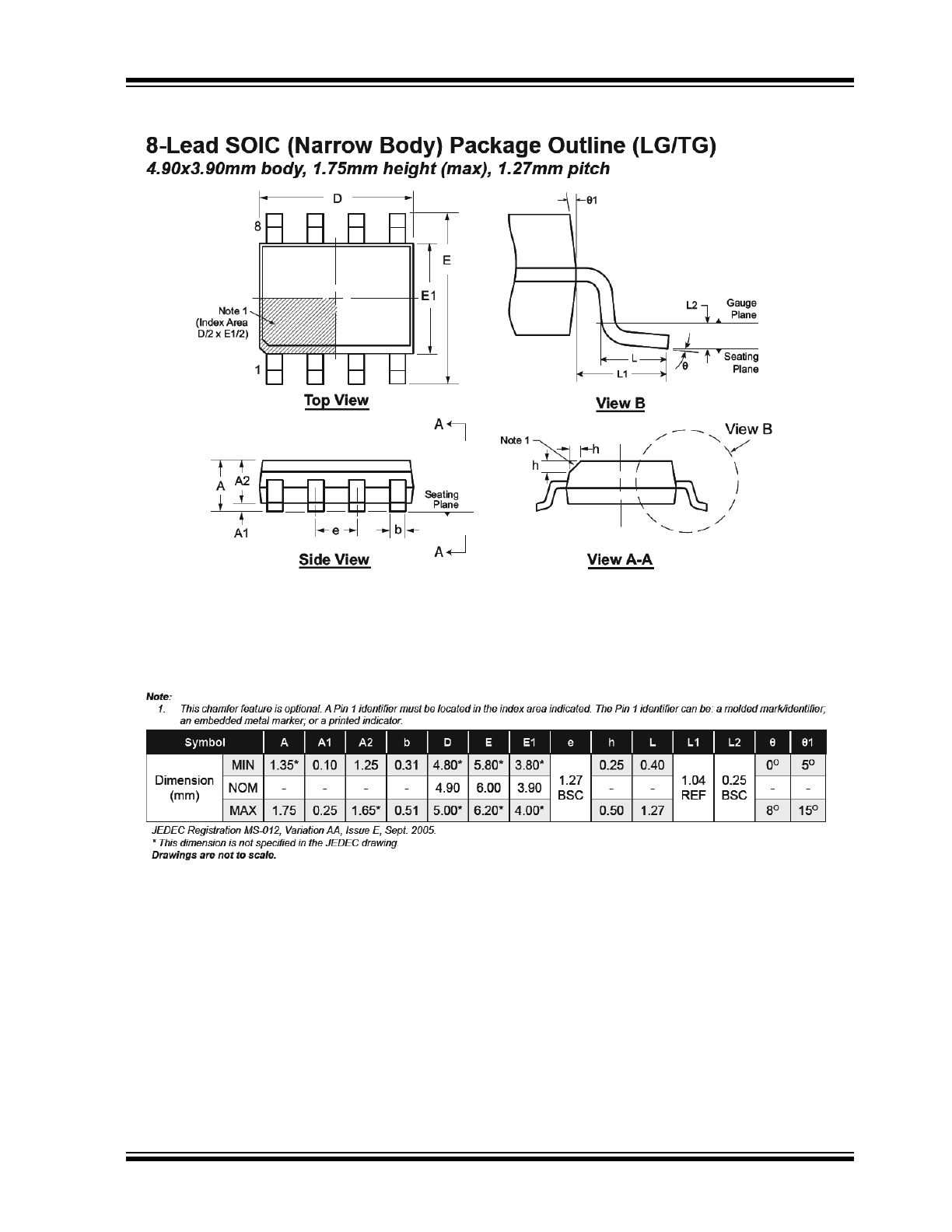
Note: For the most current package drawings, see the Microchip Packaging Specification at www.microchip.com/packaging.
LR645
DS20005384A-page 10
2015 Microchip Technology Inc.
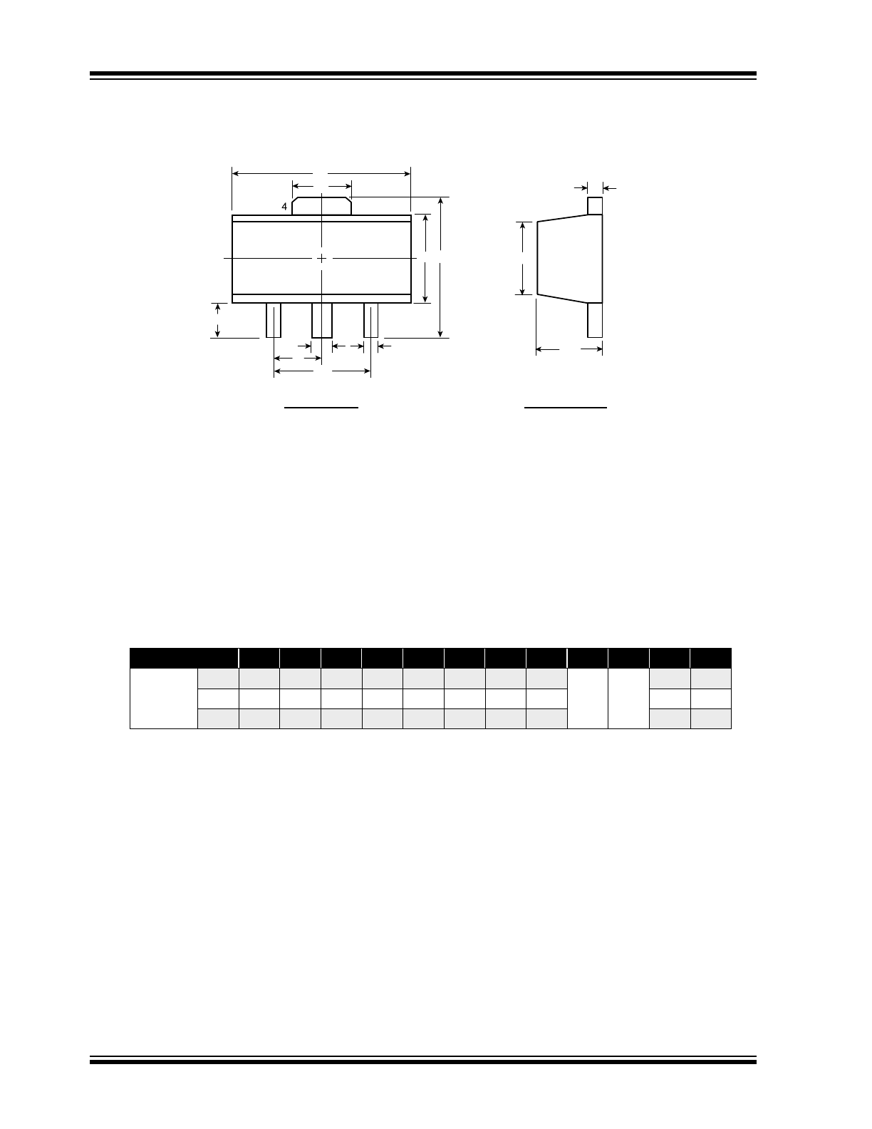
3-Lead TO-243AA (SOT-89) Package Outline (N8)
Symbol
A
b
b1
C
D
D1
E
E1
e
e1
H
L
Dimensions
(mm)
MIN
1.40
0.44
0.36
0.35
4.40
1.62
2.29
2.00
†
1.50
BSC
3.00
BSC
3.94
0.73
†
NOM
-
-
-
-
-
-
-
-
-
-
MAX
1.60
0.56
0.48
0.44
4.60
1.83
2.60
2.29
4.25
1.20
JEDEC Registration TO-243, Variation AA, Issue C, July 1986.
† This dimension differs from the JEDEC drawing
Drawings not to scale.
b
b1
D
D1
E H
E1
C
A
1
2
3
e
e1
Top View
Side View
L
Note: For the most current package drawings, see the Microchip Packaging Specification at www.microchip.com/packaging.
Note: For the most current package drawings, see the Microchip Packaging Specification at www.microchip.com/packaging.