

2015 Microchip Technology Inc.
DS20005344A-page 1
HV9910B
Features
• Switch mode controller for single switch LED drivers
• Enhanced drop-in replacement to the HV9910
• Open loop peak current controller
• Internal 8.0 to 450V linear regulator
• Constant frequency or constant off-time operation
• Linear and PWM dimming capability
• Requires few external components for operation
Applications
• DC/DC or AC/DC LED driver applications
• RGB backlighting LED driver
• Back lighting of flat panel displays
• General purpose constant current source
• Signage and decorative LED lighting
• Chargers
Description
HV9910B is an open loop, current mode control, LED
driver IC. This IC can be programmed to operate in
either a constant frequency or constant off-time mode.
It includes an 8.0 - 450V linear regulator which allows it
to work from a wide range of input voltages without the
need for an external low voltage supply. HV9910B
includes a PWM-dimming input that can accept an
external control signal with a duty ratio of 0 - 100% and
a frequency of up to a few kilohertz. It also includes a 0
- 250mV linear dimming input which can be used for lin-
ear dimming of the LED current.
HV9910B is ideally suited for buck LED drivers. Since
the HV9910B operates in open loop current mode con-
trol, the controller achieves good output current regula-
tion without the need for any loop compensation. PWM
dimming response is limited only by the rate of rise and
fall of the inductor current, enabling very fast rise and
fall times. HV9910B requires only three external com-
ponents, apart from the power stage, to produce a con-
trolled LED current. This makes HV9910B an ideal
solution for low cost LED drivers.
Universal High-Brightness LED Driver
HV9910B
DS20005344A-page 2
2015 Microchip Technology Inc.
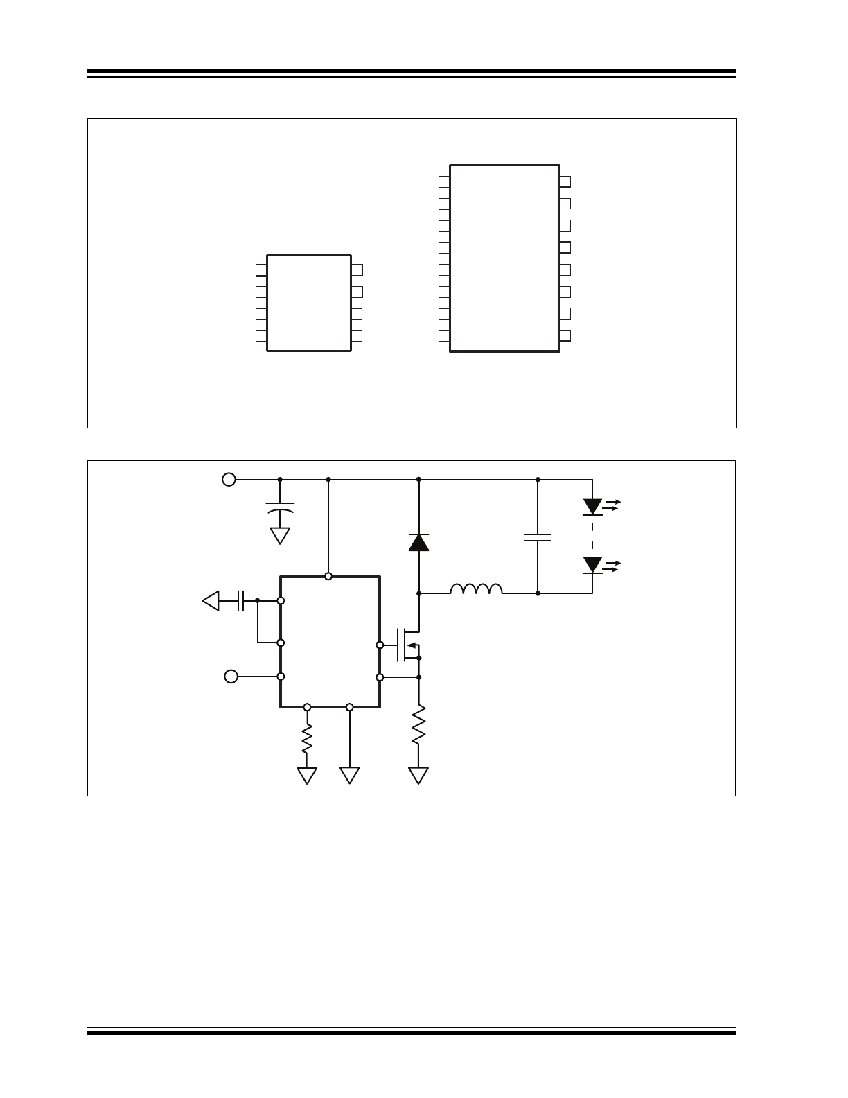
Package Type
Typical Application Circuit
8-Lead SOIC
16-Lead SOIC
1
2
3
4
5
6
7
8
16
15
14
13
12
11
10
9
8
7
6
5
1
2
3
4
VIN
CS
GND
GATE
RT
LD
VDD
PWMD
VIN
NC
NC
CS
GND
NC
NC
GATE
NC
NC
RT
LD
VDD
NC
NC
PWMD
See
Table 2-1
for pin information
C
DD
R
T
R
CS
L1
Q1
D1
C
O
C
IN
HV9910B
VIN
GATE
PWMD
VDD
LD
CS
RT
GND
2015 Microchip Technology Inc.
DS20005344A-page 3
HV9910B
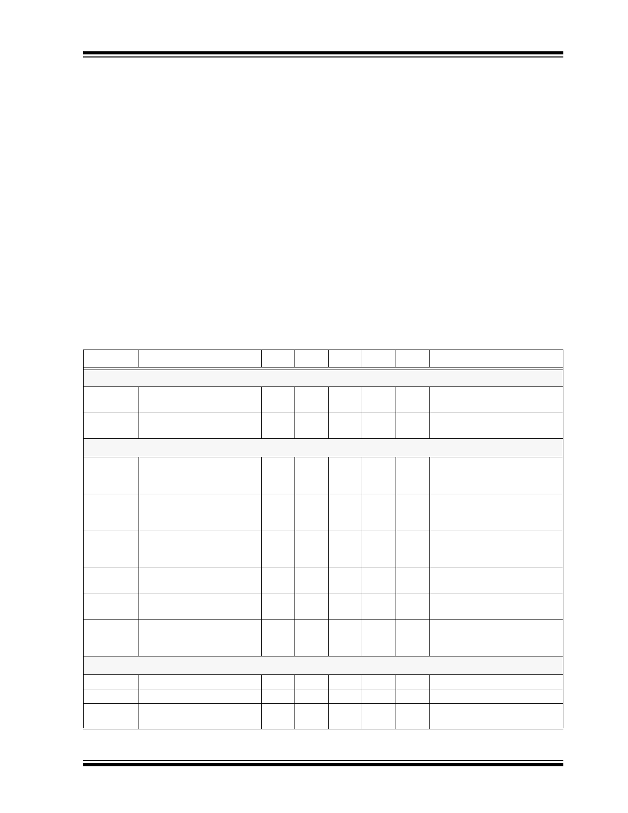
1.0
ELECTRICAL
CHARACTERISTICS
ABSOLUTE MAXIMUM RATINGS
V
IN
to GND...................................................... -0.5V to +470V
V
DD
to GND.......................................................................12V
CS, LD, PWMD, GATE, RT to GND... ....-0.3V to (V
DD
+ 0.3V)
Operating temperature..................................-40°C to +125°C
Storage temperature .....................................-65°C to +150°C
Continuous power dissipation (T
A
= +25°C)
8-lead SOIC ...............................................630 mW
16-lead SOIC ...........................................1300 mW
Note: Stresses above those listed under “Absolute Maximum
Ratings” may cause permanent damage to the device. This is
a stress rating only and functional operation of the device at
those or any other conditions, above those indicated in the
operational listings of this specification, is not implied. Expo-
sure to maximum rating conditions for extended periods may
affect device reliability.
1.1
ELECTRICAL SPECIFICATIONS
TABLE 1-1:
ELECTRICAL CHARACTERISTICS (SHEET 1 OF 2)
1
Symbol
Parameter
Note
Min
Typ
Max
Units Conditions
Input
V
INDC
Input DC supply voltage
range
2
3
8.0
-
450
V
DC input voltage
I
INSD
Shut-down mode supply
current
3
-
0.5
1.0
mA
Pin PWMD to GND
Internal Regulator
V
DD
Internally regulated voltage
-
7.25
7.5
7.75
V
V
IN
= 8.0V, I
DD(ext)
= 0, 500pF
at GATE; R
T
= 226kΩ, PWMD
= V
DD
∆V
DD, line
Line regulation of V
DD
-
0
-
1.0
V
VIN = 8.0 - 450V, I
DD(ext)
= 0,
500pF at GATE; RT = 226kΩ,
PWMD = V
DD
∆V
DD, load
Load regulation of V
DD
-
0
-
100
mV
I
DD(ext)
= 0 - 1.0mA, 500pF at
GATE; R
T
= 226kΩ, PWMD =
V
DD
UVLO
V
DD
undervoltage lockout
threshold
3
6.45
6.7
6.95
V
V
DD
rising
∆UVLO
V
DD
undervoltage lockout
hysteresis
-
-
500
-
mV
V
DD
falling
I
IN,MAX
Current that the regulator
can supply before IC goes
into UVLO
4
5.0
-
-
mA
V
IN
= 8.0V
PWM Dimming
V
EN(lo)
Pin PWMD input low voltage
3
-
-
0.8
V
V
IN
= 8.0 - 450V
V
EN(hi)
Pin PWMD input high voltage
3
2.0
-
-
V
V
IN
= 8.0 - 450V
R
EN
Pin PWMD pull-down resis-
tance at PWMD
-
50
100
150
kΩ
V
PWMD
= 5.0V
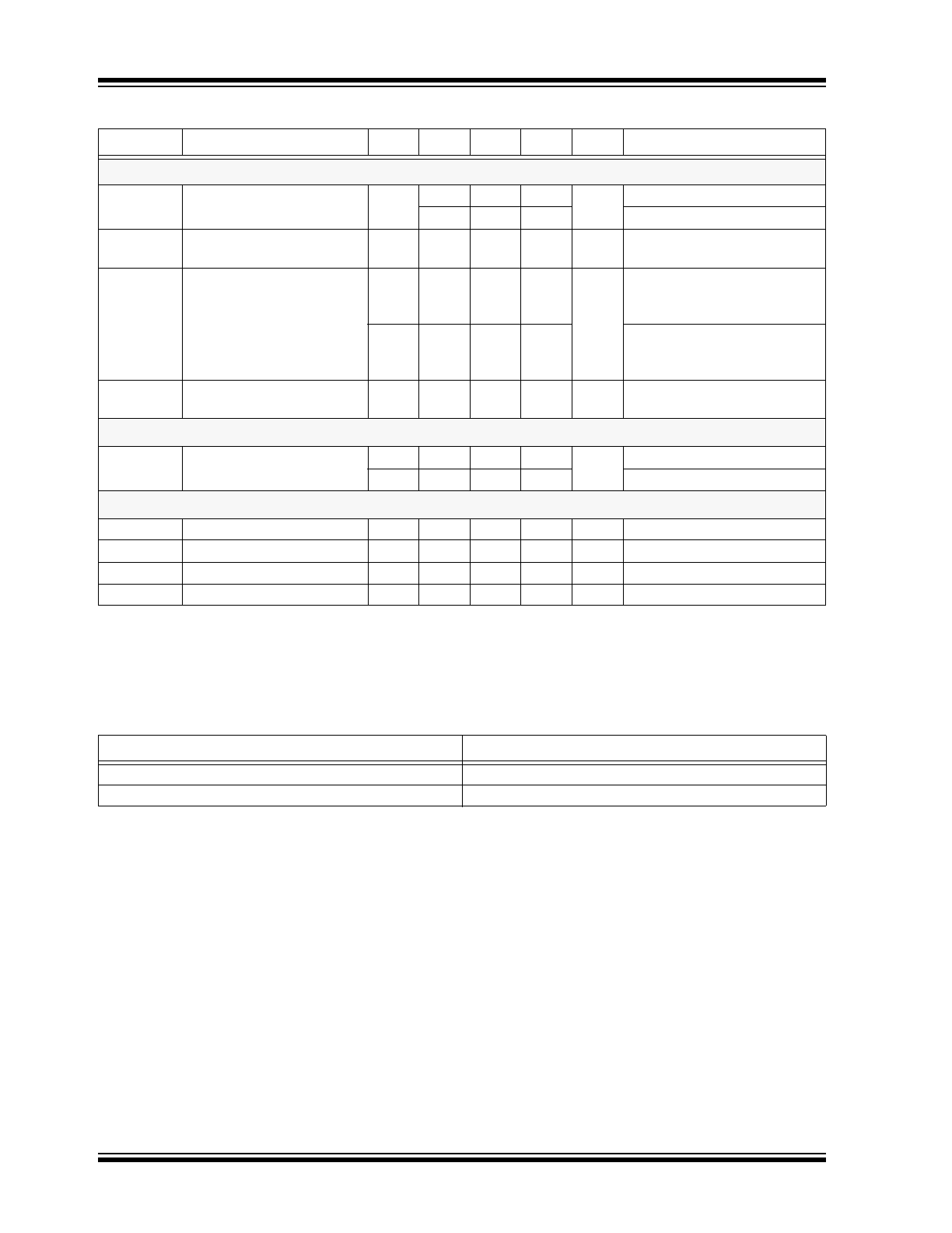
HV9910B
DS20005344A-page 4
2015 Microchip Technology Inc.
Current Sense Comparator
V
CS,TH
Current sense pull-in thresh-
old voltage
-
225
250
275
mV
-40°C < T
A
< +85°C
213
250
287
T
A
< +125°C
V
OFFSET
Offset voltage for LD com-
parator
3
-12
-
12
mV
T
BLANK
Current sense blanking
interval
-
150
215
280
ns
0 < T
A
< +85°C, V
LD
= V
DD
,
V
CS
= V
CS,TH
+ 50mV after
T
BLANK
-
145
215
315
-40 < T
A
< +125°C, V
LD
= V
DD
,
V
CS
= V
CS,TH
+ 50mV after
T
BLANK
t
DELAY
Delay to output
-
-
80
150
ns
V
LD
= V
DD
, V
CS
= V
CS,TH
+
50mV after T
BLANK
Oscillator
f
OSC
Oscillator frequency
-
20
25
30
kHz
R
T
= 1.00MΩ
-
80
100
120
R
T
= 226kΩ
Gate Driver
I
SOURCE
GATE sourcing current
-
165
-
-
mA
V
GATE
= 0V, V
DD
= 7.5V
I
SINK
GATE sinking current
-
165
-
-
mA
V
GATE
= V
DD
, V
DD
= 7.5V
t
RISE
GATE output rise time
-
-
30
50
ns
C
GATE
= 500pF, V
DD
= 7.5V
t
FALL
GATE output fall time
-
-
30
50
ns
C
GATE
= 500pF, V
DD
= 7.5V
1
Specifications are T
A
= 25°C, V
IN
= 15V unless otherwise noted.
2
Also limited by package-power dissipation limit; Whichever is lower.
3
Applies over the full operating ambient temperature range of -40°C < T
A
< +125°C.
4
For design guidance only
TABLE 1-1:
ELECTRICAL CHARACTERISTICS (CONTINUED) (SHEET 2 OF 2)
1
Symbol
Parameter
Note
Min
Typ
Max
Units Conditions
TABLE 1-2:
THERMAL RESISTANCE
Package
θja
8-Lead SOIC
101°C/W
16-Lead SOIC
83°C/W

2015 Microchip Technology Inc.
DS20005344A-page 5
HV9910B
2.0
PIN DESCRIPTION
The locations of the pins are listed in
Package Type
.
TABLE 2-1:
PIN DESCRIPTION
Pin #
Function
Description
8-Lead SOIC 16-Lead SOIC
1
1
VIN
Input of an 8.0 - 450V linear regulator.
2
4
CS
Current sense pin used to sense the FET current by means of an
external sense resistor. When this pin exceeds the lower of either
the internal 250mV or the voltage at the LD pin, the GATE output
goes low.
3
5
GND
Ground return for all internal circuitry. This pin must be electrically
connected to the ground of the power train.
4
8
GATE
Output GATE driver for an external N-channel power MOSFET.
5
9
PWMD
PWM dimming input of the IC. When this pin is pulled to GND, the
GATE driver is turned off. When the pin is pulled high, the GATE
driver operates normally.
6
12
VDD
Power supply for all internal circuits.
It must be bypassed with a low ESR capacitor to GND (≥0.1μF).
7
13
LD
Linear dimming input and sets the current sense threshold as long
as the voltage at the pin is less than 250mV (typ).
8
14
RT
Sets the oscillator frequency. When a resistor is connected
between RT and GND, the HV9910B operates in constant fre-
quency mode. When the resistor is connected between RT and
GATE, the IC operates in constant off-time mode.
-
2, 3, 6, 7, 10,
11, 15, 16
NC
No connection

HV9910B
DS20005344A-page 6
2015 Microchip Technology Inc.
3.0
APPLICATION INFORMATION
HV9910B is optimized to drive buck LED drivers using
open-loop, peak current mode control. This method of
control enables fairly accurate LED current control
without the need for high side current sensing or the
design of any closed loop controllers. The IC uses very
few external components and enables both Linear and
PWM-dimming of the LED current.
A resistor connected to the RT pin programs the fre-
quency of operation (or the off-time). The oscillator pro-
duces pulses at regular intervals. These pulses set the
SR flip-flop in the HV9910B which causes the GATE
driver to turn on. The same pulses also start the blank-
ing timer, which inhibits the reset input of the SR flip-
flop and prevent false turn-offs due to the turn-on spike.
When the FET turns on, the current through the induc-
tor starts ramping up. This current flows through the
external sense resistor R
CS
and produces a ramp volt-
age at the CS pin. The comparators are constantly
comparing the CS pin voltage to both the voltage at the
LD pin and the internal 250mV. Once the blanking timer
is complete, the output of these comparators is allowed
to reset the flip-flop. When the output of either one of
the two comparators goes high, the flip flop is reset and
the GATE output goes low. The GATE goes low until
the SR flip-flop is set by the oscillator. Assuming a 30%
ripple in the inductor, the current sense resistor RCS
can be set using:
Constant frequency peak current mode control has an
inherent disadvantage – at duty cycles greater than
0.5, the control scheme goes into subharmonic oscilla-
tions. To prevent this, an artificial slope is typically
added to the current sense waveform. This slope com-
pensation scheme will affect the accuracy of the LED
current in the present form. However, a constant off-
time peak current control scheme does not have this
problem and can easily operate at duty cycles greater
then 0.5. This control scheme also gives inherent input
voltage rejection, making the LED current almost
insensitive to input voltage variations. However, this
scheme leads to variable frequency operation and the
frequency range depends greatly on the input and out-
put voltage variation. HV9910B makes it easy to switch
between the two modes of operation by changing one
connection (see
Section 3.3 “Oscillator”
).
3.1
Input Voltage Regulator
HV9910B can be powered directly from its VIN pin and
can work from 8.0 - 450VDC at its VIN pin. When a volt-
age is applied at the VIN pin, the HV9910B maintains a
constant 7.5V at the VDD pin. This voltage is used to
power the IC and any external resistor dividers needed
to control the IC. The VDD pin must be bypassed by a
low-ESR capacitor to provide a low impedance path for
the high frequency current of the output GATE driver.
HV9910B can also be operated by supplying a voltage
at the VDD pin greater than the internally regulated
voltage. This will turn off the internal linear regulator of
the IC and the HV9910B will operate directly off the
voltage supplied at the VDD pin. Please note that this
external voltage at the VDD pin should not exceed 12V.
Although the VIN pin of the HV9910B is rated up to
450V, the actual maximum voltage that can be applied
is limited by the power dissipation in the IC. For exam-
ple, if an 8-pin SOIC (junction to ambient thermal resis-
tance R
θ,j-a
= 128°C/W) HV9910B draws about I
IN
=
2.0mA from the VIN pin, and has a maximum allowable
temperature rise of the junction temperature limited to
about ∆T = 100°C, the maximum voltage at the VIN pin
would be:
In these cases, to operate the HV9910B from higher
input voltages, a Zener diode can be added in series
with the VIN pin to divert some of the power loss from
the HV9910B to the Zener diode. In the above exam-
ple, using a 100V Zener diode will allow the circuit to
easily work up to 450V.
The input current drawn from the VIN pin is a sum of the
1.0mA current drawn by the internal circuit and the cur-
rent drawn by the GATE driver.The GATE driver
depends on the switching frequency and the GATE
charge of the external FET).
In the above equation, f
S
is the switching frequency and
QG is the GATE charge of the external FET (which can
be obtained from the data sheet of the FET).
3.2
Current Sense
The current sense input of the HV9910B goes to the
non-inverting inputs of two comparators. The inverting
terminal of one comparator is tied to an internal 250mV
reference, whereas the inverting terminal of the other
comparator is connected to the LD pin. The outputs of
both these comparators are fed into an OR GATE and
the output of the OR GATE is fed into the reset pin of
the flip-flop. Thus, the comparator which has the lowest
voltage at the inverting terminal determines when the
GATE output is turned off.
R
CS
0.25V orV
LD
1.15 I
LED
A
------------------------------------
=
V
IN MAX
T
R
j a
–
-------------- 1
I
IN
------
100
C
128
C W
---------------------------
1
2mA
-------------
390V
=
=
=
I
IN
1.0mA Q
g
f
s
+

2015 Microchip Technology Inc.
DS20005344A-page 7
HV9910B
The outputs of the comparators also include a 150-
280ns blanking time which prevents spurious turn-offs
of the external FET due to the turn-on spike normally
present in peak current mode control. In rare cases,
this internal blanking might not be enough to filter out
the turn-on spike. In these cases, an external RC filter
needs to be added between the external sense resistor
(RCS) and the CS pin.
Please note that the comparators are fast with a typical
80ns response time. Hence these comparators are
more susceptible to be triggered by noise than the
comparators of the HV9910. A proper layout minimiz-
ing external inductances will prevent false triggering of
these comparators.
3.3
Oscillator
The oscillator in the HV9910B is controlled by a single
resistor connected at the RT pin. The equation govern-
ing the oscillator time period t
OSC
is given by:
If the resistor is connected between RT and GND,
HV9910B operates in a constant frequency mode and
the above equation determines the time-period. If the
resistor is connected between RT and GATE, the
HV9910B operates in a constant off-time mode and the
above equation determines the off-time.
3.4
Gate Output
The GATE output of the HV9910B is used to drive an
external FET. It is recommended that the GATE charge
of the external FET be less than 25nC for switching fre-
quencies ≤100kHz and less than 15nC for switching
frequencies > 100kHz.
3.5
Linear Dimming
The Linear Dimming pin is used to control the LED cur-
rent. There are two cases when it may be necessary to
use the Linear Dimming pin.
1.
In some cases, when using the internal 250mV,
it may not be possible to find the exact RCS
value required to obtain the LED current. In
these cases, an external voltage divider from the
VDD pin can be connected to the LD pin to
obtain a voltage (less than 250mV) correspond-
ing to the desired voltage across R
CS
.
2.
Linear dimming may be desired to adjust the
current level to reduce the intensity of the LEDs.
In these cases, an external 0-250mV voltage
can be connected to the LD pin to adjust the
LED current during operation.
To use the internal 250mV, the LD pin can be con-
nected to VDD.
3.6
PWM Dimming
PWM Dimming can be achieved by driving the PWMD
pin with a low frequency square wave signal. When the
PWM signal is zero, the GATE driver is turned off; when
the PWMD signal if high, the GATE driver is enabled.
The PWMD signal does not turn off the other parts of
the IC, therefore, the response of the HV9910B to the
PWMD signal is almost instantaneous. The rate of rise
and fall of the LED current is thus determined solely by
the rise and fall times of the inductor current.
To disable PWM dimming and enable the HV9910B
permanently, connect the PWMD pin to VDD.
t
OSC
s
R
T
k
22
+
25
---------------------------------
=
Note:
Although the LD pin can be pulled to GND,
the output current will not go to zero. This
is due to the presence of a minimum on-
time, which is equal to the sum of the
blanking time and the delay to output time,
or about 450ns. This minimum on-time
causes the FET to be on for a minimum of
450ns, and thus the LED current when LD
= GND is not zero. This current is also
dependent on the input voltage, induc-
tance value, forward voltage of the LEDs,
and circuit parasitics. To get zero LED cur-
rent, the PWMD pin has to be used.
HV9910B
DS20005344A-page 8
2015 Microchip Technology Inc.
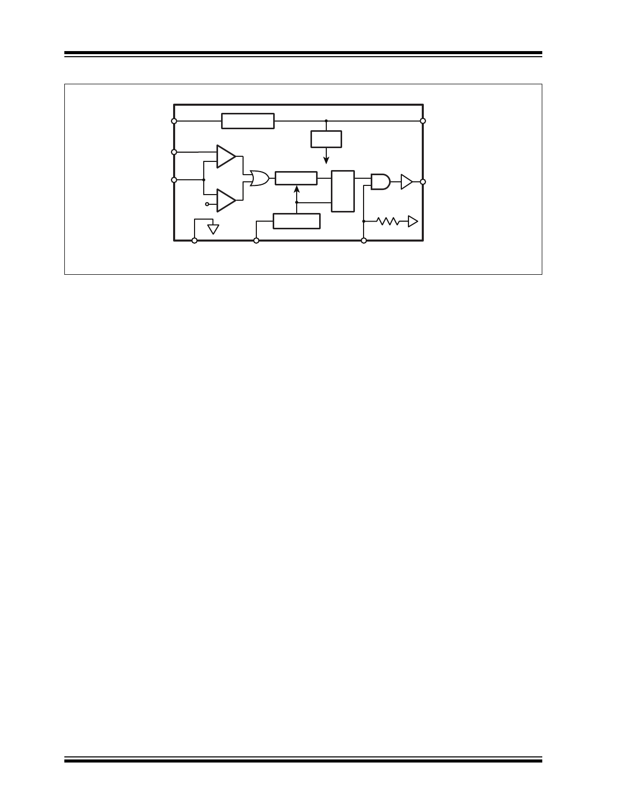
FIGURE 3-1:
INTERNAL BLOCK DIAGRAM
POR
250mV
RT
PWMD
GATE
VDD
VIN
LD
CS
GND
Blanking
Oscillator
Regulator
+
-
+
-
S
R Q
2015 Microchip Technology Inc.
DS20005344A-page 9
HV9910B
4.0
PACKAGING INFORMATION
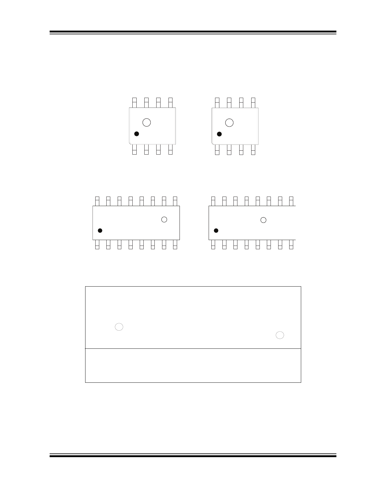
4.1
Package Marking Information
Legend: XX...X
Product Code or Customer-specific information
Y
Year code (last digit of calendar year)
YY
Year code (last 2 digits of calendar year)
WW
Week code (week of January 1 is week ‘01’)
NNN
Alphanumeric traceability code
Pb-free JEDEC
®
designator for Matte Tin (Sn)
*
This package is Pb-free. The Pb-free JEDEC designator ( )
can be found on the outer packaging for this package.
Note:
In the event the full Microchip part number cannot be marked on one line, it will
be carried over to the next line, thus limiting the number of available
characters for product code or customer-specific information. Package may or
not include the corporate logo.
3
e
3
e
8-lead SOIC
Example
NNN
XX
XXXXXXXX
YYWW
e3
343
LG
HV9910B
1447
e3
16-lead SOIC
XXXXXXXXX
XXXXXXXXXXX
YYWWNNN
e3
Example
HV9910BNG
1447343
e3
HV9910B
DS20005344A-page 10
2015 Microchip Technology Inc.
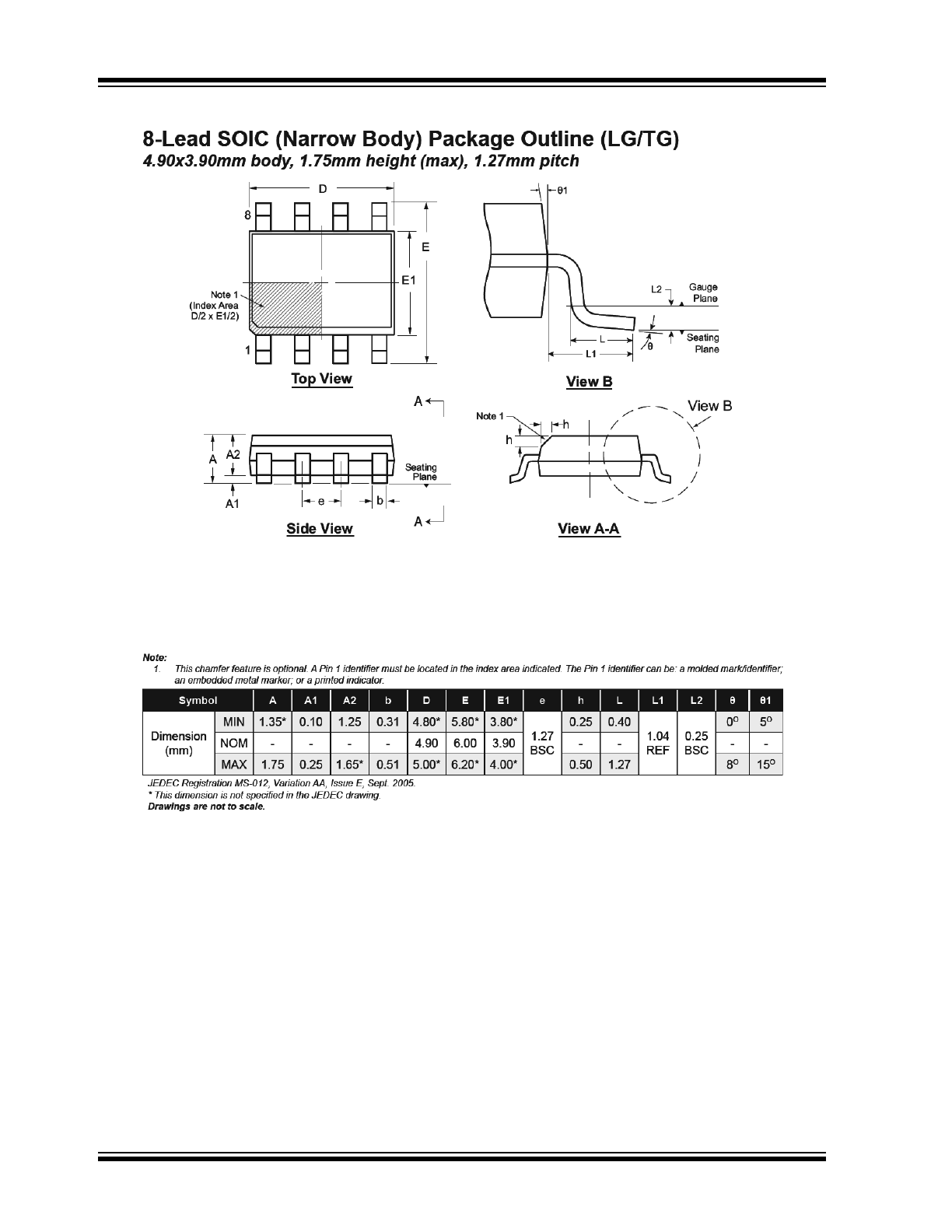
Note: For the most current package drawings, see the Microchip Packaging Specification at www.microchip.com/packaging.