
© 2009 Microchip Technology Inc.
DS22003E-page 1
MCP3421
Features
• 18-bit
ΔΣ
ADC in a SOT-23-6 package
• Differential Input Operation
• Self Calibration of Internal Offset and Gain Per
Each Conversion
• On-Board Voltage Reference:
- Accuracy: 2.048V ± 0.05%
- Drift: 15 ppm/°C
• On-Board Programmable Gain Amplifier (PGA):
- Gains of 1,2, 4 or 8
• On-Board Oscillator
• INL: 10 ppm of FSR (FSR = 4.096V/PGA)
• Programmable Data Rate Options:
- 3.75 SPS (18 bits)
- 15 SPS (16 bits)
- 60 SPS (14 bits)
- 240 SPS (12 bits)
• One-Shot or Continuous Conversion Options
• Low Current Consumption:
- 145 µA typical
(V
DD
= 3V, Continuous Conversion)
- 39 µA typical
(V
DD
= 3V, One-Shot Conversion with 1 SPS)
• Supports I
2
C Serial Interface:
- Standard, Fast and High Speed Modes
• Single Supply Operation: 2.7V to 5.5V
• Extended Temperature Range: -40°C to +125°C
Typical Applications
• Portable Instrumentation
• Weigh Scales and Fuel Gauges
• Temperature Sensing with RTD, Thermistor, and
Thermocouple
• Bridge Sensing for Pressure, Strain, and Force.
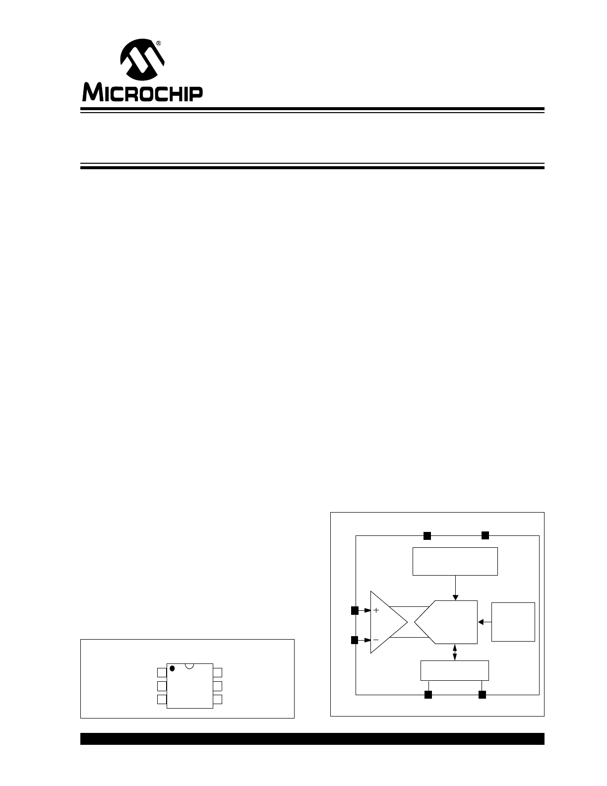
Package Types
Description
The MCP3421 is a single channel low-noise, high
accuracy
ΔΣ A/D converter with differential inputs and
up to 18 bits of resolution in a small SOT-23-6 package.
The on-board precision 2.048V reference voltage
enables an input range of ±2.048V differentially
(
Δ voltage = 4.096V). The device uses a two-wire I
2
C
compatible serial interface and operates from a single
2.7V to 5.5V power supply.
The MCP3421 device performs conversion at rates of
3.75, 15, 60, or 240 samples per second (SPS)
depending on the user controllable configuration bit
settings using the two-wire I
2
C serial interface. This
device has an on-board programmable gain amplifier
(PGA). The user can select the PGA gain of x1, x2, x4,
or x8 before the analog-to-digital conversion takes
place. This allows the MCP3421 device to convert a
smaller input signal with high resolution. The device
has two conversion modes: (a) Continuous mode and
(b) One-Shot mode. In One-Shot mode, the device
enters a low current standby mode automatically after
one conversion. This reduces current consumption
greatly during idle periods.
The MCP3421 device can be used for various high
accuracy analog-to-digital data conversion applications
where design simplicity, low power, and small footprint
are major considerations.
Block Diagram
1
2
3
4
5
6
V
IN
+
V
SS
SCL
V
IN
-
V
DD
SDA
MCP3421
SOT-23-6
V
SS
V
DD
V
IN
+
V
IN
-
SCL
SDA
Voltage Reference
Clock
(2.048V)
I
2
C Interface
Gain = 1, 2, 4, or 8
V
REF
ΔΣ ADC
Converter
PGA
Oscillator
18-Bit Analog-to-Digital Converter
with I
2
C Interface and On-Board Reference

MCP3421
DS22003E-page 2
© 2009 Microchip Technology Inc.
NOTES:
© 2009 Microchip Technology Inc.
DS22003E-page 3
MCP3421
1.0
ELECTRICAL
CHARACTERISTICS
1.1
Absolute Maximum Ratings†
V
DD
...................................................................................7.0V
All inputs and outputs w.r.t V
SS
............... –0.3V to V
DD
+0.3V
Differential Input Voltage ...................................... |V
DD
- V
SS
|
Output Short Circuit Current ................................ Continuous
Current at Input Pins ....................................................±2 mA
Current at Output and Supply Pins ............................±10 mA
Storage Temperature ....................................-65°C to +150°C
Ambient Temp. with power applied ...............-55°C to +125°C
ESD protection on all pins
................ ≥ 6 kV HBM, ≥ 400V MM
Maximum Junction Temperature (T
J
) . .........................+150°C
†Notice: Stresses above those listed under “Maximum Rat-
ings” may cause permanent damage to the device. This is a
stress rating only and functional operation of the device at
those or any other conditions above those indicated in the
operational listings of this specification is not implied.
Exposure to maximum rating conditions for extended periods
may affect device reliability
.
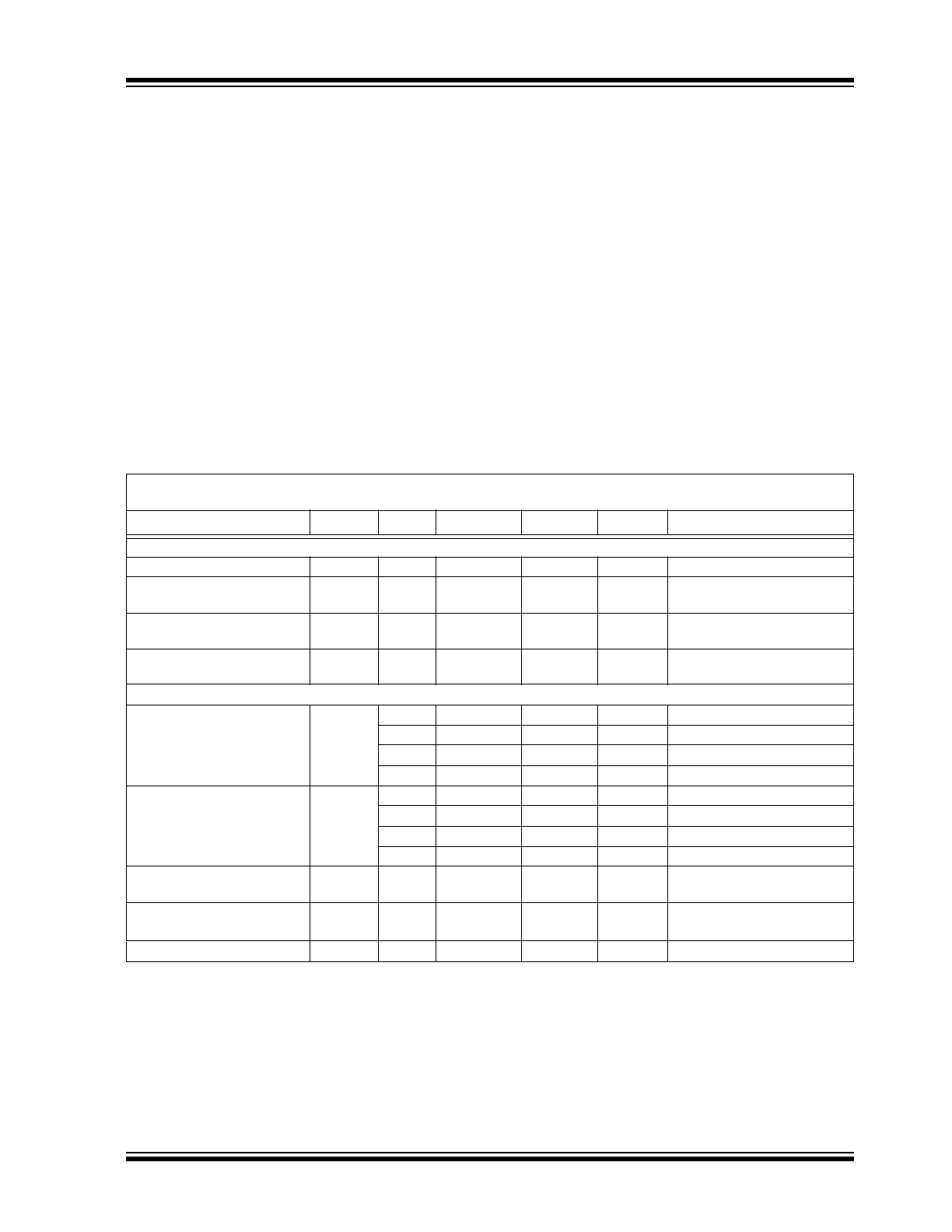
1.2
Electrical Specifications
ELECTRICAL CHARACTERISTICS
Electrical Specifications: Unless otherwise specified, all parameters apply for T
A
= -40°C to +85°C, V
DD
= +5.0V, V
SS
= 0V,
V
IN
+ = V
IN
- = V
REF
/2. All ppm units use 2*V
REF
as full scale range.
Parameters
Sym
Min
Typ
Max
Units
Conditions
Analog Inputs
Differential Input Range
—
±2.048/PGA
—
V
V
IN
= V
IN
+ - V
IN
-
Common-Mode Voltage Range
(absolute)
(Note 1)
V
SS
-0.3
—
V
DD
+0.3
V
Differential Input Impedance
(Note 2)
Z
IND
(f)
—
2.25/PGA
—
M
Ω
During normal mode operation
Common Mode input
Impedance
Z
INC
(f)
—
25
—
M
Ω
PGA = 1, 2, 4, 8
System Performance
Resolution and No Missing
Codes
(Note 8)
12
—
—
Bits
DR = 240 SPS
14
—
—
Bits
DR = 60 SPS
16
—
—
Bits
DR = 15 SPS
18
—
—
Bits
DR = 3.75 SPS
Data Rate
(Note 3)
DR
176
240
328
SPS
S1,S0 = ‘00’, (12 bits mode)
44
60
82
SPS
S1,S0 = ‘01’, (14 bits mode)
11
15
20.5
SPS
S1,S0 = ‘10’, (16 bits mode)
2.75
3.75
5.1
SPS
S1,S0 = ‘11’, (18 bits mode)
Output Noise
—
1.5
—
µV
RMS
T
A
= +25°C, DR = 3.75 SPS,
PGA = 1, V
IN
= 0
Integral Nonlinearity
(Note 4)
INL
—
10
35
ppm of
FSR
DR = 3.75 SPS
(Note 6)
Internal Reference Voltage
V
REF
—
2.048
—
V
Note 1:
Any input voltage below or greater than this voltage causes leakage current through the ESD diodes at the input pins.
This parameter is ensured by characterization and not 100% tested.
2:
This input impedance is due to 3.2 pF internal input sampling capacitor.
3:
The total conversion speed includes auto-calibration of offset and gain.
4:
INL is the difference between the endpoints line and the measured code at the center of the quantization band.
5:
Includes all errors from on-board PGA and V
REF
.
6:
Full Scale Range (FSR) = 2 x 2.048/PGA = 4.096/PGA.
7:
This parameter is ensured by characterization and not 100% tested.
8:
This parameter is ensured by design and not 100% tested.
MCP3421
DS22003E-page 4
© 2009 Microchip Technology Inc.
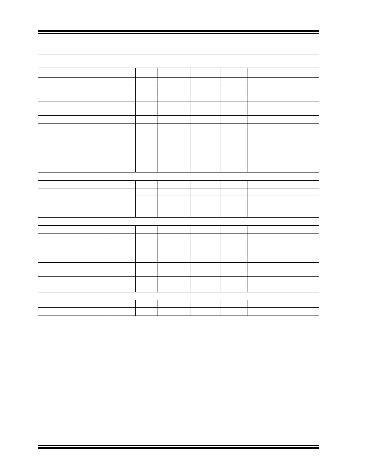
Gain Error
(Note 5)
—
0.05
0.35
%
PGA = 1, DR = 3.75 SPS
PGA Gain Error Match
(Note 5)
—
0.1
—
%
Between any 2 PGA gains
Gain Error Drift
(Note 5)
—
15
—
ppm/°C
PGA=1, DR=3.75 SPS
Offset Error
V
OS
—
15
40
µV
Tested at PGA = 1
V
DD
= 5.0V and DR = 3.75 SPS
Offset Drift vs. Temperature
—
50
—
nV/°C
V
DD
= 5.0V
Common-Mode Rejection
—
105
—
dB
at DC and PGA =1,
—
110
—
dB
at DC and PGA =8,
T
A
= +25°C
Gain vs. V
DD
—
5
—
ppm/V
T
A
= +25°C, V
DD
= 2.7V to 5.5V,
PGA = 1
Power Supply Rejection at DC
—
100
—
dB
T
A
= +25°C, V
DD
= 2.7V to 5.5V,
PGA = 1
Power Requirements
Voltage Range
V
DD
2.7
—
5.5
V
Supply Current during
Conversion
I
DDA
—
155
190
µA
V
DD
= 5.0V
—
145
—
µA
V
DD
= 3.0V
Supply Current during Standby
Mode
I
DDS
—
0.1
0.5
µA
I
2
C Digital Inputs and Digital Outputs
High level input voltage
V
IH
0.7 V
DD
—
V
DD
V
Low level input voltage
V
IL
—
—
0.3V
DD
V
Low level output voltage
V
OL
—
—
0.4
V
I
OL
= 3 mA, V
DD
= +5.0V
Hysteresis of Schmitt Trigger
for inputs
(Note 7)
V
HYST
0.05V
DD
—
—
V
f
SCL
= 100 kHz
Supply Current when I
2
C bus
line is active
I
DDB
—
—
10
µA
Input Leakage Current
I
ILH
—
—
1
µA
V
IH
= 5.5V
I
ILL
-1
—
—
µA
V
IL
= GND
Pin Capacitance and I
2
C Bus Capacitance
Pin capacitance
C
PIN
—
—
10
pF
I
2
C Bus Capacitance
C
b
—
—
400
pF
ELECTRICAL CHARACTERISTICS (CONTINUED)
Electrical Specifications: Unless otherwise specified, all parameters apply for T
A
= -40°C to +85°C, V
DD
= +5.0V, V
SS
= 0V,
V
IN
+ = V
IN
- = V
REF
/2. All ppm units use 2*V
REF
as full scale range.
Parameters
Sym
Min
Typ
Max
Units
Conditions
Note 1:
Any input voltage below or greater than this voltage causes leakage current through the ESD diodes at the input pins.
This parameter is ensured by characterization and not 100% tested.
2:
This input impedance is due to 3.2 pF internal input sampling capacitor.
3:
The total conversion speed includes auto-calibration of offset and gain.
4:
INL is the difference between the endpoints line and the measured code at the center of the quantization band.
5:
Includes all errors from on-board PGA and V
REF
.
6:
Full Scale Range (FSR) = 2 x 2.048/PGA = 4.096/PGA.
7:
This parameter is ensured by characterization and not 100% tested.
8:
This parameter is ensured by design and not 100% tested.
© 2009 Microchip Technology Inc.
DS22003E-page 5
MCP3421
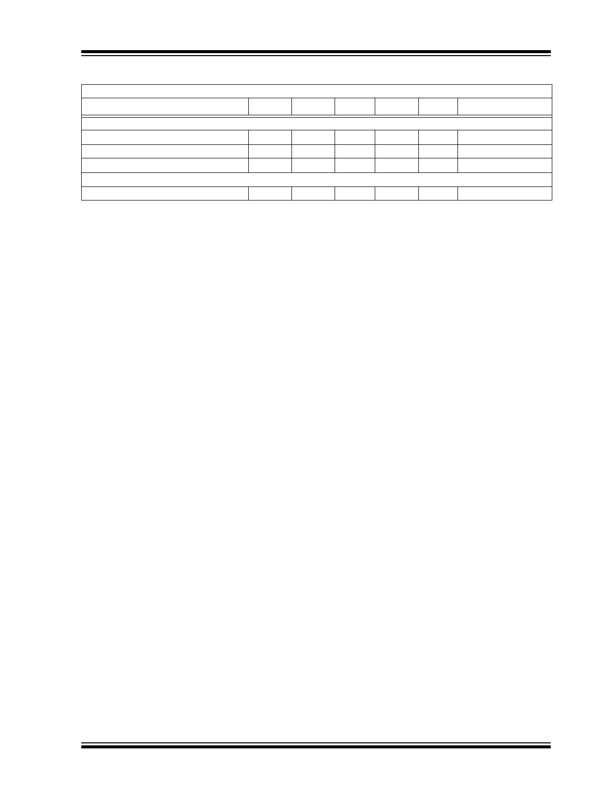
TEMPERATURE SPECIFICATIONS
Electrical Characteristics: Unless otherwise indicated, T
A
= -40°C to +85°C, V
DD
= +5.0V, V
SS
= 0V.
Parameters
Sym
Min
Typ
Max
Units
Conditions
Temperature Ranges
Specified Temperature Range
T
A
-40
—
+85
°C
Operating Temperature Range
T
A
-40
—
+125
°C
Storage Temperature Range
T
A
-65
—
+150
°C
Thermal Package Resistances
Thermal Resistance, 6L SOT-23
θ
JA
—
190.5
—
°C/W

MCP3421
DS22003E-page 6
© 2009 Microchip Technology Inc.
NOTES:
© 2009 Microchip Technology Inc.
DS22003E-page 7
MCP3421
2.0
TYPICAL PERFORMANCE CURVES
Note: Unless otherwise indicated, T
A
= -40°C to +85°C, V
DD
= +5.0V, V
SS
= 0V, V
IN
+ = V
IN
- = V
REF
/2.
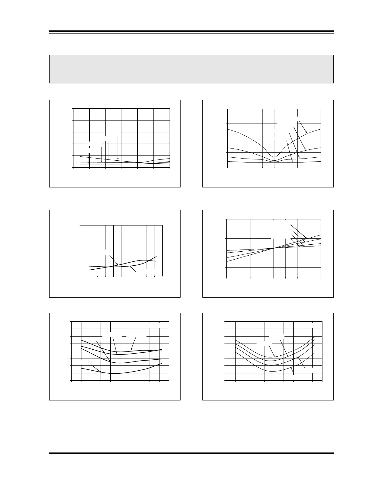
FIGURE 2-1:
INL vs. Supply Voltage
(V
DD
).
FIGURE 2-2:
INL vs. Temperature.
FIGURE 2-3:
Offset Error vs.
Temperature.
FIGURE 2-4:
Output Noise vs. Input
Voltage.
FIGURE 2-5:
Total Error vs. Input Voltage.
FIGURE 2-6:
Gain Error vs. Temperature.
Note:
The graphs and tables provided following this note are a statistical summary based on a limited number of
samples and are provided for informational purposes only. The performance characteristics listed herein
are not tested or guaranteed. In some graphs or tables, the data presented may be outside the specified
operating range (e.g., outside specified power supply range) and therefore outside the warranted range.
.000
.001
.002
.003
.004
.005
2.5
3
3.5
4
4.5
5
5.5
V
DD
(V)
PGA = 1
PGA = 2
PGA = 8
PGA = 4
Integra
l Nonlinea
rity
(% of FSR
)
0
0.001
0.002
0.003
-60 -40 -20 0
20 40 60 80 100 120 140
Temperature (
o
C)
Inte
gral Nonline
a
rity
(% of FSR)
V
DD
= 5 V
V
DD
= 2.7V
PGA = 1
-20
-15
-10
-5
0
5
10
15
20
-60 -40 -20
0
20
40
60
80 100 120 140
Temperature (°C)
O
ffset Er
ro
r (µ
V)
V
DD
= 5V
PGA = 1
PGA = 2
PGA = 8
PGA = 4
0.0
2.5
5.0
7.5
10.0
-100 -75
-50
-25
0
25
50
75
100
Input Voltage (% of Full Scale)
N
o
is
e (
µ
V
, r
m
s)
PGA = 1
PGA = 2
PGA = 8
PGA = 4
T
A
= +25°C
V
DD
= 5V
-3.0
-2.0
-1.0
0.0
1.0
2.0
3.0
-100 -75
-50
-25
0
25
50
75
100
Input Voltage (% of Full Scale)
T
o
ta
l E
rro
r
(m
V
)
PGA = 1
PGA = 2
PGA = 8
PGA = 4
-0.4
-0.3
-0.2
-0.1
0
0.1
0.2
0.3
0.4
-60 -40 -20
0
20
40
60
80 100 120 140
Temperature (°C)
Gain
Err
o
r (% o
f FSR
)
V
DD
= 5.0V
PGA = 1
PGA = 2
PGA = 8
PGA = 4
MCP3421
DS22003E-page 8
© 2009 Microchip Technology Inc.
Note: Unless otherwise indicated, T
A
= -40°C to +85°C, V
DD
= +5.0V, V
SS
= 0V, V
IN
+ = V
IN
- = V
REF
/2.
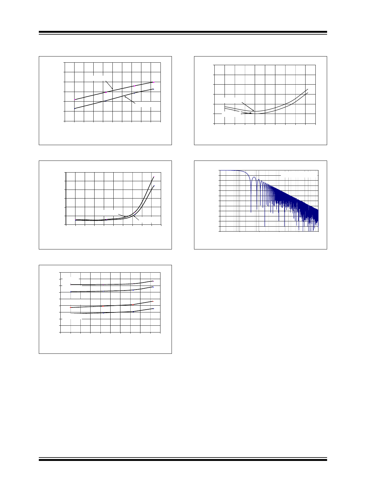
FIGURE 2-7:
I
DDA
vs. Temperature.
FIGURE 2-8:
I
DDS
vs. Temperature.
FIGURE 2-9:
I
DDB
vs. Temperature.
FIGURE 2-10:
OSC Drift vs. Temperature.
FIGURE 2-11:
Frequency Response.
100
120
140
160
180
200
220
-60 -40 -20
0
20 40 60 80 100 120 140
Temperature (
o
C)
I
DD
A
(µ
A)
V
DD
= 5V
V
DD
= 2.7V
0
100
200
300
400
500
600
-60 -40 -20 0
20 40 60 80 100 120 140
Temperature (
o
C)
I
DD
S
(nA)
V
DD
= 2.7V
V
DD
= 5V
0
1
2
3
4
5
6
7
8
9
-60 -40 -20
0
20 40 60 80 100 120 140
Temperature (
o
C)
I
DDB
(
μ
A)
V
DD
= 5V
V
DD
= 4.5V
V
DD
= 3.3V
V
DD
= 2.7V
-1
0
1
2
3
4
5
-60 -40 -20
0
20
40
60
80 100 120 140
Temperature (°C)
Osc
illator Drift (%)
V
DD
= 5.0V
V
DD
= 2.7V
Data Rate = 3.75 SPS
-120
-110
-100
-90
-80
-70
-60
-50
-40
-30
-20
-10
0
0.1
1
10
100
1000
10000
Input Signal Frequency (Hz)
Magnit
u
d
e (d
B)
0.1
1
10
100
1k
10k
© 2009 Microchip Technology Inc.
DS22003E-page 9
MCP3421
3.0
PIN DESCRIPTIONS
The descriptions of the pins are listed in
Table 3-1
.
TABLE 3-1:
PIN FUNCTION TABLE
3.1
Analog Inputs (V
IN
+, V
IN
-)
V
IN
+ and V
IN
- are differential signal input pins. The
MCP3421 device accepts a fully differential analog
input signal which is connected on the V
IN
+ and V
IN
-
input pins. The differential voltage that is converted is
defined by V
IN
= (V
IN
+ - V
IN
-) where V
IN
+ is the voltage
applied at the V
IN
+ pin and V
IN
- is the voltage applied
at the V
IN
- pin. The user can also connect V
IN
-
pin to
V
SS
for a single-ended operation. See
Figure 6-4
for
differential and single-ended connection examples.
The input signal level is amplified by the programmable
gain amplifier (PGA) before the conversion. The
differential input voltage should not exceed an absolute
of (V
REF
/PGA) for accurate measurement, where V
REF
is the internal reference voltage (2.048V) and PGA is
the PGA gain setting. The converter output code will
saturate if the input range exceeds (V
REF
/PGA).
The absolute voltage range on each of the differential
input pins is from V
SS
-0.3V to V
DD
+0.3V. Any voltage
above or below this range will cause leakage currents
through the Electrostatic Discharge (ESD) diodes at
the input pins. This ESD current can cause unexpected
performance of the device. The common mode of the
analog inputs should be chosen such that both the
differential analog input range and the absolute voltage
range on each pin are within the specified operating
range defined in
Section 1.0 “Electrical
Characteristics” and Section 4.0 “Description of
Device Operation”.
See
Section 4.5 “Input Voltage Range” for more
details of the input voltage range.
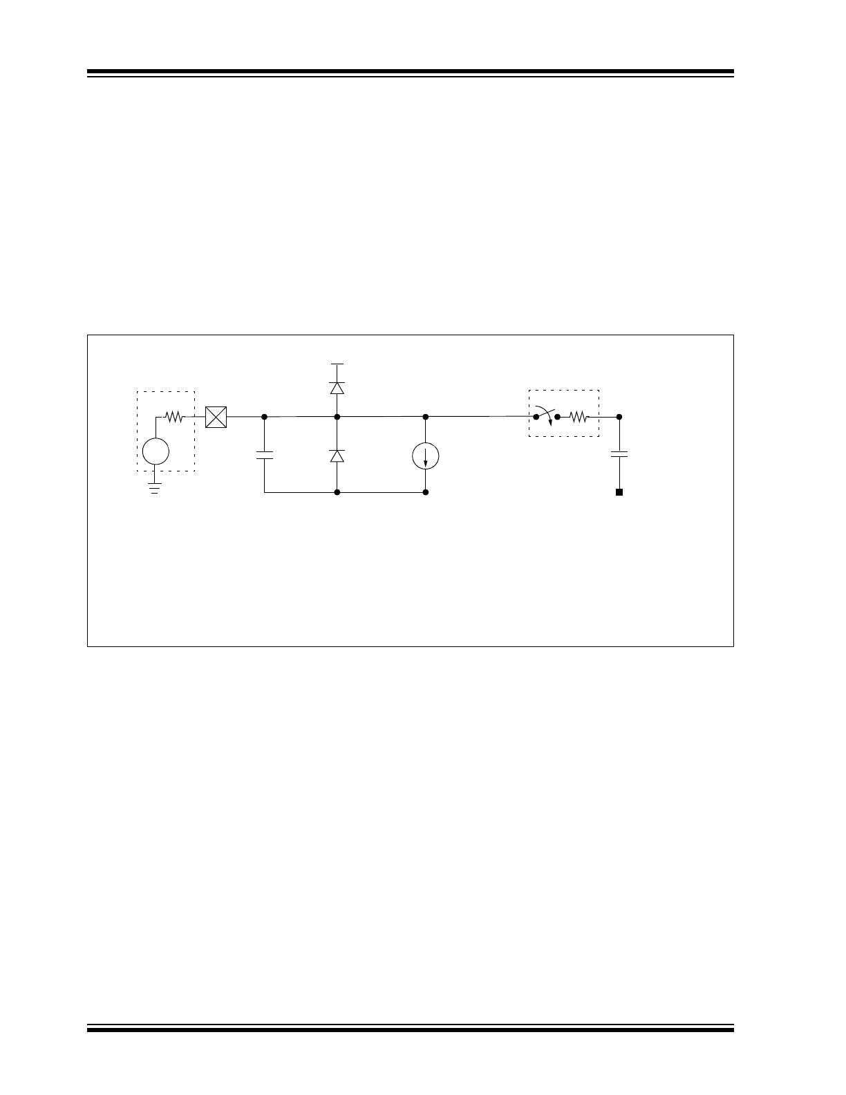
Figure 3-1
shows the input structure of the device. The
device uses a switched capacitor input stage at the
front end. C
PIN
is the package pin capacitance and
typically about 4 pF. D
1
and D
2
are the ESD diodes.
C
SAMPLE
is the differential input sampling capacitor.
3.2
Supply Voltage (V
DD
, V
SS
)
V
DD
is the power supply pin for the device. This pin
requires an appropriate bypass capacitor of about
0.1 µF (ceramic) to ground. An additional 10 µF
capacitor (tantalum) in parallel is also recommended
to further attenuate high frequency noise present in
some application boards. The supply voltage (V
DD
)
must be maintained in the 2.7V to 5.5V range for
specified operation.
V
SS
is the ground pin and the current return path of the
device. The user must connect the V
SS
pin to a ground
plane through a low impedance connection. If an
analog ground path is available in the application PCB
(printed circuit board), it is highly recommended that
the V
SS
pin be tied to the analog ground path or
isolated within an analog ground plane of the circuit
board.
3.3
Serial Clock Pin (SCL)
SCL is the serial clock pin of the I
2
C interface. The
MCP3421 acts only as a slave and the SCL pin
accepts only external serial clocks. The input data
from the Master device is shifted into the SDA pin on
the rising edges of the SCL clock and output from the
MCP3421 occurs at the falling edges of the SCL clock.
The SCL pin is an open-drain N-channel driver.
Therefore, it needs a pull-up resistor from the V
DD
line
to the SCL pin. Refer to
Section 5.3 “I
2
C Serial
Communications” for more details of I
2
C Serial
Interface communication.
MCP3421
Symbol
Description
1
V
IN
+
Positive Differential Analog Input Pin
2
V
SS
Ground Pin
3
SCL
Serial Clock Input Pin of the I
2
C Interface
4
SDA
Bidirectional Serial Data Pin of the I
2
C Interface
5
V
DD
Positive Supply Voltage Pin
6
V
IN
-
Negative Differential Analog Input Pin
MCP3421
DS22003E-page 10
© 2009 Microchip Technology Inc.
3.4
Serial Data Pin (SDA)
SDA is the serial data pin of the I
2
C interface. The SDA
pin is used for input and output data. In read mode, the
conversion result is read from the SDA pin (output). In
write mode, the device configuration bits are written
(input) though the SDA pin. The SDA pin is an open-
drain N-channel driver. Therefore, it needs a pull-up
resistor from the V
DD
line to the SDA pin. Except for
start and stop conditions, the data on the SDA pin must
be stable during the high period of the clock. The high
or low state of the SDA pin can only change when the
clock signal on the SCL pin is low. Refer to
Section 5.3
“I
2
C Serial Communications” for more details of I
2
C
Serial Interface communication.
Typical range of the pull-up resistor value for SCL and
SDA is from 5 k
Ω to 10 kΩ for standard (100 kHz) and
fast (400 kHz) modes, and less than 1 k
Ω for high
speed mode (3.4 MHz). The High-Speed mode is not
recommended for V
DD
less than 2.7V.
FIGURE 3-1:
Equivalent Analog Input Circuit.
C
PIN
V
R
SS
V
IN
+,V
IN
-
4 pF
V
T
= 0.6V
V
T
= 0.6V
I
LEAKAGE
Sampling
Switch
SS
R
S
C
SAMPLE
(3.2 pF)
V
DD
(~ ±1 nA)
Legend:
V
=
Signal Source
I
LEAKAGE
=
Leakage Current at Analog Pin
R
SS
=
Source Impedance
SS
=
Sampling Switch
V
IN
+, V
IN
-
=
Analog Input Pin
R
S
=
Sampling Switch Resistor
C
PIN
=
Input Pin Capacitance
C
SAMPLE
=
Sample Capacitance
V
T
=
Threshold Voltage
D
1
, D
2
=
ESD Protection Diode
D
1
D
2
V
SS