
1996-2013 Microchip Technology Inc.
Preliminary
DS40143E-page 1
PIC16C55X
Devices Included in this Data Sheet:
Referred to collectively as PIC16C55X.
• PIC16C554
• PIC16C557
• PIC16C558
High Performance RISC CPU:
• Only 35 instructions to learn
• All single-cycle instructions (200 ns), except for
program branches which are two-cycle
• Operating speed:
- DC - 20 MHz clock input
- DC - 20 ns instruction cycle
• Interrupt capability
• 16-18 special function hardware registers
• 8-level deep hardware stack
• Direct, Indirect and Relative Addressing modes
Peripheral Features:
• 13-22 I/O pins with individual direction control
- Pull-up resistors on PORTB
• High current sink/source for direct LED drive
• Timer0: 8-bit timer/counter with 8-bit programma-
ble prescaler
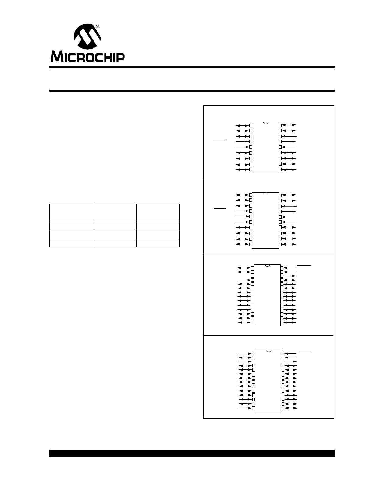
Pin Diagram
Device
Program
Memory
Data Memory
PIC16C554
512
80
PIC16C557
2 K
128
PIC16C558
2 K
128
RA1
RA0
OSC2/CLKOUT
V
DD
RB7
RB6
RB5
RB4
OSC1/CLKIN
RA2
RA3
MCLR/Vpp
V
SS
RB0/INT
RB1
RB2
RB3
RA4/T0CKI
PIC
1
6C
5
5
4/
558
PDIP, SOIC, Windowed CERDIP
SSOP
2
3
4
5
6
7
8
9
•1
18
17
15
14
13
12
11
10
16
RA1
RA0
OSC2/CLKOUT
V
DD
RB7
RB6
RB5
OSC1/CLKIN
RA2
RA3
MCLR/V
PP
V
SS
RB1
RB2
RA4/T0CKI
PI
C
16C
5
5
7
RB4
RB3
2
3
4
5
6
7
8
9
10
•1
19
18
16
15
14
13
12
11
17
20
21
22
23
24
25
26
27
28
N/C
RA5
RB0/INT
RC7
RC6
RC5
RC4
RC3
RC2
RC1
RC0
PDIP, SOIC, Windowed CERDIP
RA1
RA0
OSC2/CLKOUT
V
DD
RB7
RB6
RB5
OSC1/CLKIN
RA2
RA3
MCLR/V
PP
V
SS
RB1
RB2
RA4/T0CKI
PIC
1
6
C
557
RB4
RB3
2
3
4
5
6
7
8
9
10
•1
19
18
16
15
14
13
12
11
17
20
21
22
23
24
25
26
27
28
RA5
RB0/INT
RC7
RC6
RC5
RC4
RC3
RC2
RC1
RC0
SSOP
V
SS
RA1
RA0
OSC2/CLKOUT
V
DD
RB7
RB6
RB5
RB4
OSC1/CLKIN
RA2
RA3
MCLR/Vpp
V
SS
RB0/INT
RB1
RB2
RB3
RA4/T0CKI
P
IC
16C
5
54/
558
2
3
4
5
6
7
8
9
•1
20
19
17
15
14
13
12
11
18
V
SS
10
V
DD
16
EPROM-Based 8-Bit CMOS Microcontrollers
PIC16C55X
DS40143E-page 2
Preliminary
1996-2013 Microchip Technology Inc.
Special Microcontroller Features:
• Power-on Reset (POR)
• Power-up Timer (PWRT) and Oscillator Start-up
Timer (OST)
• Watchdog Timer (WDT) with its own on-chip RC
oscillator for reliable operation
• Programmable code protection
• Power saving SLEEP mode
• Selectable oscillator options
• Serial in-circuit programming (via two pins)
• Four user programmable ID locations
CMOS Technology:
• Low power, high speed CMOS EPROM technol-
ogy
• Fully static design
• Wide operating voltage range
- 2.5V to 5.5V
• Commercial, Industrial and Extended temperature
range
• Low power consumption
- < 2.0 mA @ 5.0V, 4.0 MHz
- 15
A typical 3.0V, 32 kHz
- < 1.0
A typical standby current @ 3.0V
Device Differences
Note:
For additional information on enhance-
ments, see Appendix A
Device
Voltage Range
Oscillator
PIC16C554
2.5 - 5.5
(Note 1)
PIC16C557
2.5 - 5.5
(Note 1)
PIC16C558
2.5 - 5.5
(Note 1)
Note 1: If you change from this device to another device, please verify oscillator characteristics in your application.

1996-2013 Microchip Technology Inc.
Preliminary
DS40143E-page 3
PIC16C55X
Table of Contents
1.0
General Description...................................................................................................................................................................... 5
2.0
PIC16C55X Device Varieties ....................................................................................................................................................... 7
3.0
Architectural Overview ................................................................................................................................................................. 9
4.0
Memory Organization ................................................................................................................................................................. 13
5.0
I/O Ports ..................................................................................................................................................................................... 23
6.0
Special Features of the CPU...................................................................................................................................................... 31
7.0
Timer0 Module ........................................................................................................................................................................... 47
8.0
Instruction Set Summary ............................................................................................................................................................ 53
9.0
Development Support................................................................................................................................................................. 67
10.0 Electrical Specifications.............................................................................................................................................................. 73
11.0 Packaging Information................................................................................................................................................................ 87
Appendix A:
Enhancements............................................................................................................................................................. 97
Appendix B:
Compatibility ............................................................................................................................................................... 97
Index .................................................................................................................................................................................................... 99
On-Line Support................................................................................................................................................................................. 101
Systems Information and Upgrade Hot Line ...................................................................................................................................... 101
Reader Response .............................................................................................................................................................................. 102
Product Identification System ............................................................................................................................................................ 103
TO OUR VALUED CUSTOMERS
It is our intention to provide our valued customers with the best documentation possible to ensure successful use of your Microchip
products. To this end, we will continue to improve our publications to better suit your needs. Our publications will be refined and
enhanced as new volumes and updates are introduced.
If you have any questions or comments regarding this publication, please contact the Marketing Communications Department via
E-mail at docerrors@mail.microchip.com or fax the Reader Response Form in the back of this data sheet to (480) 792-4150.
We welcome your feedback.
Most Current Data Sheet
To obtain the most up-to-date version of this data sheet, please register at our Worldwide Web site at:
http://www.microchip.com
You can determine the version of a data sheet by examining its literature number found on the bottom outside corner of any page.
The last character of the literature number is the version number, (e.g., DS30000A is version A of document DS30000).
Errata
An errata sheet, describing minor operational differences from the data sheet and recommended workarounds, may exist for current
devices. As device/documentation issues become known to us, we will publish an errata sheet. The errata will specify the revision
of silicon and revision of document to which it applies.
To determine if an errata sheet exists for a particular device, please check with one of the following:
• Microchip’s Worldwide Web site; http://www.microchip.com
• Your local Microchip sales office (see last page)
• The Microchip Corporate Literature Center; U.S. FAX: (480) 792-7277
When contacting a sales office or the literature center, please specify which device, revision of silicon and data sheet (include liter-
ature number) you are using.
Customer Notification System
Register on our web site at www.microchip.com/cn to receive the most current information on all of our products.

PIC16C55X
DS40143E-page 4
Preliminary
1996-2013 Microchip Technology Inc.
NOTES:

1996-2013 Microchip Technology Inc.
Preliminary
DS40143E-page 5
PIC16C55X
1.0
GENERAL DESCRIPTION
The PIC16C55X are 18, 20 and 28-Pin EPROM-based
members of the versatile PIC16CXX family of low cost,
high performance, CMOS, fully-static, 8-bit
microcontrollers.
All PIC
®
microcontrollers employ an advanced RISC
architecture. The PIC16C55X have enhanced core fea-
tures, eight-level deep stack, and multiple internal and
external interrupt sources. The separate instruction
and data buses of the Harvard architecture allow a 14-
bit wide instruction word with the separate 8-bit wide
data. The two-stage instruction pipeline allows all
instructions to execute in a single-cycle, except for pro-
gram branches (which require two cycles). A total of 35
instructions (reduced instruction set) are available.
Additionally, a large register set gives some of the
architectural innovations used to achieve a very high
performance.
PIC16C55X microcontrollers typically achieve a 2:1
code compression and a 4:1 speed improvement over
other 8-bit microcontrollers in their class.
The PIC16C554 has 80 bytes of RAM. The PIC16C557
and PIC16C558 have 128 bytes of RAM. The
PIC16C554 and PIC16C558 have 13 I/O pins and an 8-
bit timer/counter with an 8-bit programmable prescaler.
The PIC16C557 has 22 I/O pins and an 8-bit timer/
counter with an 8-bit programmable prescaler.
PIC16C55X devices have special features to reduce
external components, thus reducing cost, enhancing
system reliability and reducing power consumption.
There are four oscillator options, of which the single pin
RC oscillator provides a low cost solution, the LP
oscillator minimizes power consumption, XT is a
standard crystal, and the HS is for high speed crystals.
The SLEEP (power-down) mode offers power saving.
The user can wake-up the chip from SLEEP through
several external and internal interrupts and RESET.
A highly reliable Watchdog Timer, with its own on-chip
RC oscillator, provides protection against software
lock-up.
A UV-erasable CERDIP packaged version is ideal for
code development while the cost effective One-Time
Programmable (OTP) version is suitable for production
in any volume.
Table 1-1 shows the features of the PIC16C55X mid-
range microcontroller families.
A simplified block diagram of the PIC16C55X is shown
in Figure 3-1.
The PIC16C55X series fit perfectly in applications
ranging from motor control to low power remote sen-
sors. The EPROM technology makes customization of
application programs (detection levels, pulse genera-
tion, timers, etc.) extremely fast and convenient. The
small footprint packages make this microcontroller
series perfect for all applications with space limitations.
Low cost, low power, high performance, ease of use
and I/O flexibility make the PIC16C55X very versatile.
1.1
Family and Upward Compatibility
Users familiar with the family of microcontrollers will
realize that this is an enhanced version of the architec-
ture. Please refer to Appendix A for a detailed list of
enhancements. Code written for can be easily ported
to PIC16C55X family of devices (Appendix B).
The PIC16C55X family fills the niche for users wanting
to migrate up from the family and not needing various
peripheral features of other members of the PIC16XX
mid-range microcontroller family.
1.2
Development Support
The PIC16C55X family is supported by a full-featured
macro assembler, a software simulator, an in-circuit
emulator, a low cost development programmer and a
full-featured programmer.

PIC16C55X
DS40143E-page 6
Preliminary
1996-2013 Microchip Technology Inc.
TABLE 1-1:
PIC16C55X FAMILY OF DEVICES
PIC16C554
PIC16C557
PIC16C558
Clock
Maximum Frequency of Operation
(MHz)
20
20
20
Memory
EPROM Program Memory
(x14 words)
512
2K
2K
Data Memory (bytes)
80
128
128
Peripherals
Timer Module(s)
TMR0
TMR0
TMR0
Features
Interrupt Sources
3
3
3
I/O Pins
13
22
13
Voltage Range (Volts)
2.5-5.5
2.5-5.5
2.5-5.5
Brown-out Reset
—
—
—
Packages
18-pin DIP, SOIC;
20-pin SSOP
28-pin DIP, SOIC;
28-pin SSOP
18-pin DIP, SOIC,
SSOP
All PIC
®
Family devices have Power-on Reset, selectable Watchdog Timer, selectable code protect and high
I/O current capability. All PIC16C55X Family devices use serial programming with clock pin RB6 and data pin RB7.

1996-2013 Microchip Technology Inc.
Preliminary
DS40143E-page 7
PIC16C55X
2.0
PIC16C55X
DEVICE VARIETIES
A variety of frequency ranges and packaging options
are available. Depending on application and production
requirements, the proper device option can be selected
using the information in the PIC16C55X Product
Identification System section at the end of this data
sheet. When placing orders, please use this page of
the data sheet to specify the correct part number.
2.1
UV Erasable Devices
The UV erasable version, offered in CERDIP package,
is optimal for prototype development and pilot
programs. This version can be erased and
reprogrammed to any of the oscillator modes.
Microchip's PICSTART
and PROMATE
programmers both support programming of the
PIC16C55X.
2.2
One-Time Programmable (OTP)
Devices
The availability of OTP devices is especially useful for
customers who need the flexibility for frequent code
updates and small volume applications. In addition to
the program memory, the configuration bits must also
be programmed.
2.3
Quick-Turnaround Production
(QTP) Devices
Microchip offers a QTP Programming Service for
factory production orders. This service is made
available for users who choose not to program a
medium-to-high quantity of units and whose code pat-
terns have stabilized. The devices are identical to the
OTP devices, but with all EPROM locations and config-
uration options already programmed by the factory.
Certain code and prototype verification procedures
apply before production shipments are available.
Please contact your Microchip Technology sales office
for more details.
2.4
Serialized Quick-Turnaround
Production (SQTP
SM
) Devices
Microchip offers a unique programming service where
a few user-defined locations in each device are
programmed with different serial numbers. The serial
numbers may be random, pseudo-random or
sequential.
Serial programming allows each device to have a
unique number which can serve as an entry code,
password or ID number.

PIC16C55X
DS40143E-page 8
Preliminary
1996-2013 Microchip Technology Inc.
NOTES:

1996-2013 Microchip Technology Inc.
Preliminary
DS40143E-page 9
PIC16C55X
3.0
ARCHITECTURAL OVERVIEW
The high performance of the PIC16C55X family can be
attributed to a number of architectural features
commonly found in RISC microprocessors. To begin
with, the PIC16C55X uses a Harvard architecture in
which program and data are accessed from separate
memories using separate busses. This improves
bandwidth over traditional von Neumann architecture
where program and data are fetched from the same
memory. Separating program and data memory further
allows instructions to be sized differently from 8-bit
wide data words. Instruction opcodes are 14-bit wide
making it possible to have all single word instructions.
A 14-bit wide program memory access bus fetches a
14-bit instruction in a single cycle. A two-stage pipeline
overlaps fetch and execution of instructions.
Consequently, all instructions (35) execute in a single-
cycle (200 ns @ 20 MHz) except for program branches.
The table below lists the memory (EPROM and RAM).
The PIC16C554 addresses 512 x 14 on-chip program
memory. The PIC16C557 and PIC16C558 addresses
2 K x 14 program memory. All program memory is inter-
nal.
The PIC16C55X can directly or indirectly address its
register files or data memory. All special function
registers, including the program counter, are mapped
into the data memory. The PIC16C55X has an orthog-
onal (symmetrical) instruction set that makes it possible
to carry out any operation on any register using any
Addressing mode. This symmetrical nature and lack of
‘special optimal situations’ make programming with the
PIC16C55X simple yet efficient. In addition, the
learning curve is reduced significantly.
The PIC16C55X devices contain an 8-bit ALU and
working register. The ALU is a general purpose
arithmetic unit. It performs arithmetic and Boolean
functions between data in the working register and any
register file.
The ALU is 8-bits wide and capable of addition,
subtraction, shift and logical operations. Unless
otherwise mentioned, arithmetic operations are two's
complement in nature. In two-operand instructions,
typically one operand is the working register
(W register). The other operand is a file register or an
immediate constant. In single operand instructions, the
operand is either the W register or a file register.
The W register is an 8-bit working register used for ALU
operations. It is not an addressable register.
Depending on the instruction executed, the ALU may
affect the values of the Carry (C), Digit Carry (DC), and
Zero (Z) bits in the STATUS register. The C and DC bits
operate as a Borrow and Digit Borrow out bit,
respectively, in subtraction. See the SUBLW and SUBWF
instructions for examples.
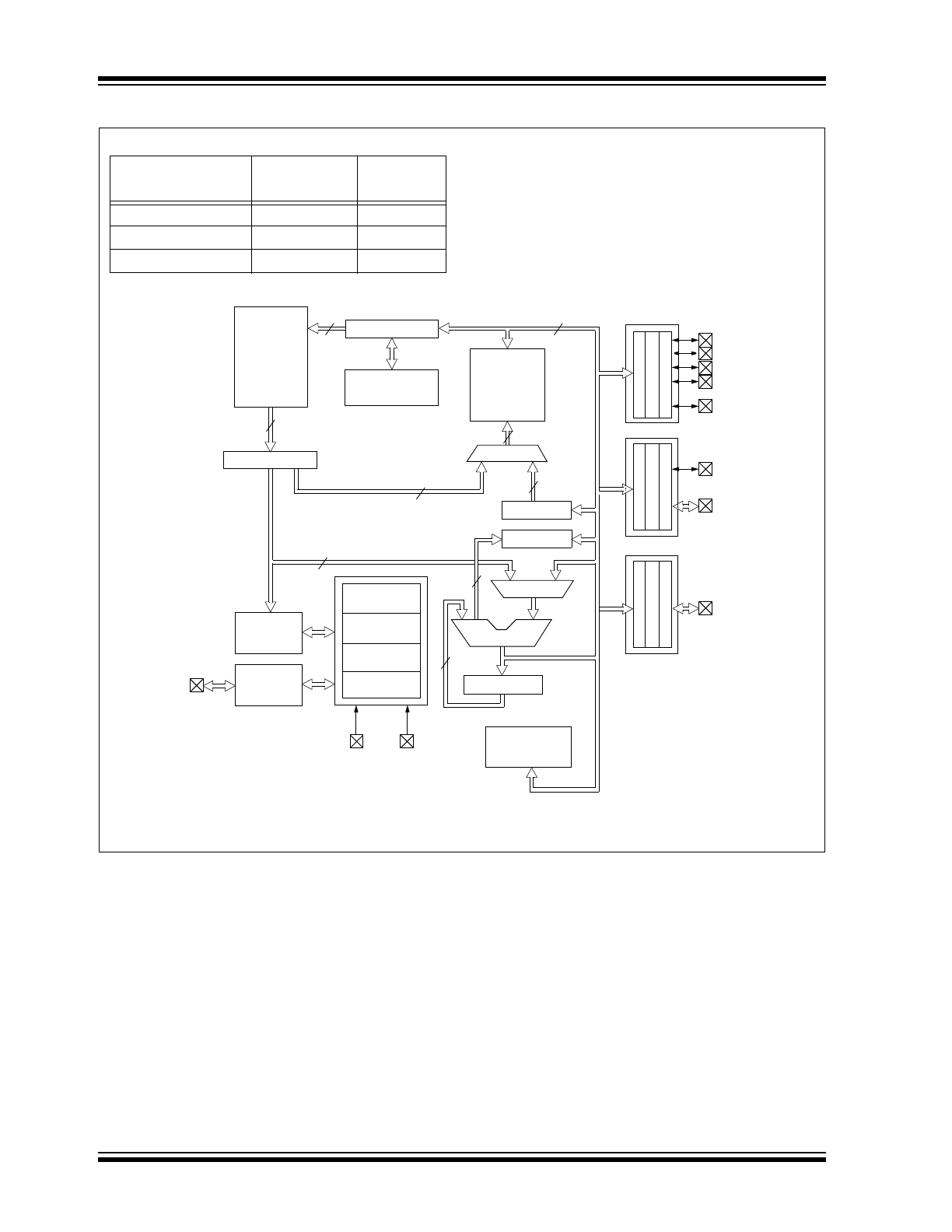
A simplified block diagram is shown in Figure 3-1, with
a description of the device pins in Table 3-1.
Device
Program
Memory
(EPROM)
Data
Memor
(RAM)
PIC16C554
512
80
PIC16C557
2 K
128
PIC16C558
2 K
128
PIC16C55X
DS40143E-page 10
Preliminary
1996-2013 Microchip Technology Inc.
FIGURE 3-1:
BLOCK DIAGRAM
EPROM
Program
Memory
2K x 14
13
Data Bus
8
14
Program
Bus
Instruction reg
Program Counter
8-Level Stack
(13-bit)
RAM
File
Registers
128 x 8
Direct Addr
7
8
Addr MUX
Indirect
Addr
8
FSR
STATUS reg
MUX
ALU
W reg
Power-up
Timer
Oscillator
Start-up Timer
Power-on
Reset
Watchdog
Timer
Instruction
Decode &
Control
Timing
Generation
OSC1/CLKIN
OSC2/CLKOUT
V
PP
V
DD
, V
SS
Timer0
3
PORTA
PORTB
RA1
RA4/T0CKI
RB0/INT
RB7:RB1
8
8
RAM Addr
(1)
RA0
RA2
RA3
512 x 14
to
80 x 8 to
Device
Program
Memory
Data
Memory
PIC16C554
512 x 14
80 x 8
PIC16C557
2 K x 14
128 x 8
PIC16C558
2 K x 14
128 x 8
PORTC
(2)
RC7:RC0
Note
1:
Higher order bits are from STATUS Register.
2:
PIC16C557 only.