
2002 Microchip Technology Inc.
DS21410B-page 1
TC3401
Features
• 16-bit Resolution at Eight Conversions Per
Second, Adjustable Down to 10-bit Resolution at
512 Conversions Per Second
• 1.8V – 5.5V Operation, Low Power Operating
300
µ
A; Sleep: 50
µ
A
• microPort™ Serial Bus Requires only two
Interface Lines
• Uses Internal or External Reference
• Automatically Enters Sleep Mode when not in use
• True Differential Inputs with Built-In Multiplexer
Provide Ratiometric Conversions
• Early Warning Power Fail Detector, also suitable as
Wake-Up Timer Operational in Shutdown Mode
• V
DD
Monitor and Reset Generator Operational in
Shutdown Mode
Applications
• Consumer Electronics, Thermostats, CO
Monitors, Humidity Meters, Security Sensors
• Embedded Systems, Data Loggers,
Portable Equipment
• Medical Instruments
Device Selection Table
Package Type
General Description
The TC3401 is a low cost, low power analog-to-digital
converter based on Microchip’s Sigma-Delta technol-
ogy. It will perform 16-bit conversions (15-bit plus sign)
at up to eight per second. The TC3401 is optimized for
use as a microcontroller peripheral in low cost, battery
operated systems. A voltage reference is included, or
an external reference can be used. A V
DD
monitor with
a reset generator provides Power-on Reset and Brown-
out protection while an extra threshold detector is suit-
able for use as an early warning Power Fail detector, or
as a Wake-up Timer.
The TC3401’s 2-wire microPort™ digital interface is
used for starting conversions and for reading out the
data. Driving the SCLK line low starts a conversion.
After the conversion starts, each additional falling edge
(up to six) detected on SCLK for t
4
seconds reduces
the A/D resolution by one bit and cuts conversion time
in half. After a conversion is completed, clocking the
SCLK line puts the MSB through LSB of the resulting
data word onto the SDAT line, much like a shift register.
The part automatically sleeps when not performing a
data conversion.
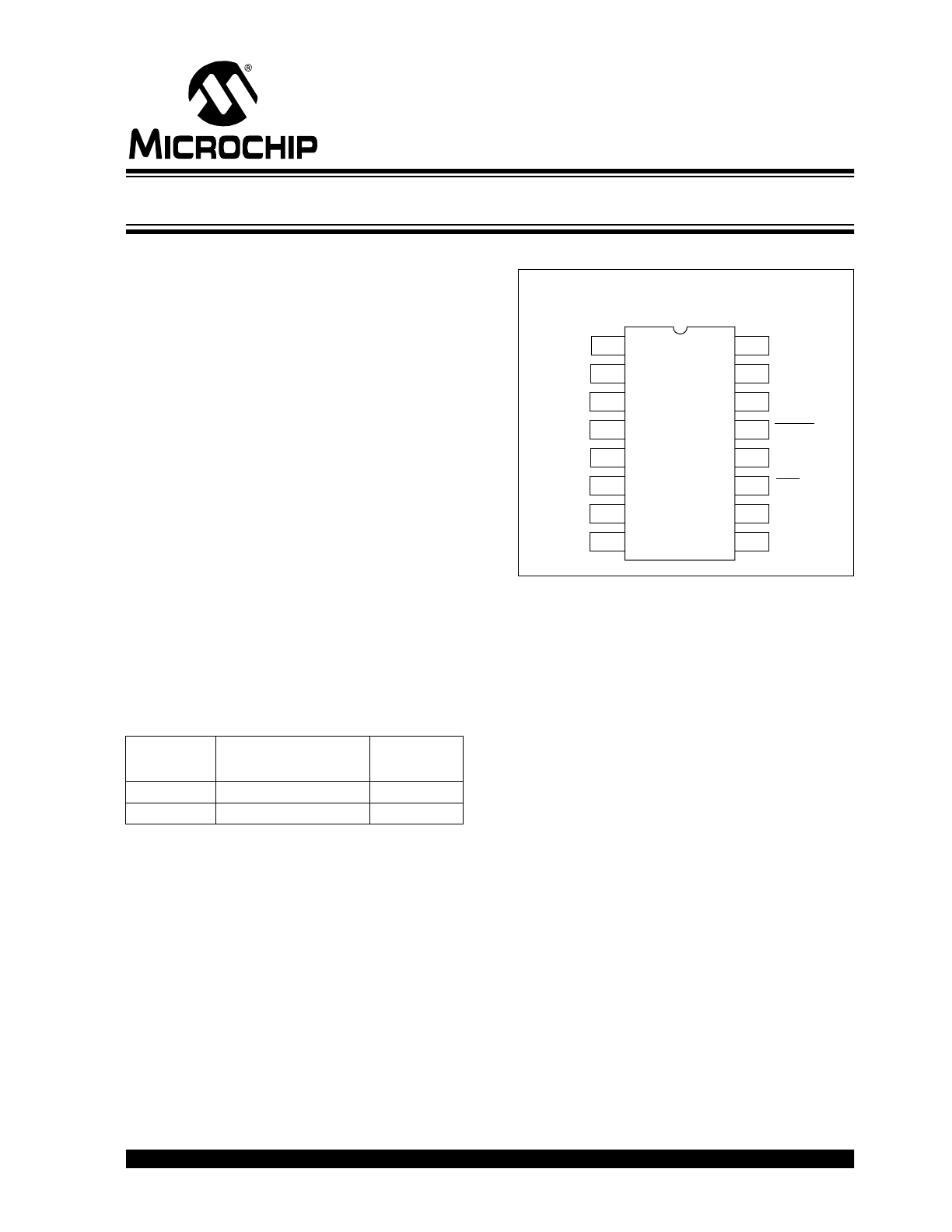
The TC3401 is available in a 16-Pin PDIP and a 16-Pin
QSOP package.
Part
Number
Package
Temperature
Range
TC3401VPE
16-Pin PDIP (Narrow)
0
°
C to +85
°
C
TC3401VQR
16-Pin QSOP Narrow)
0
°
C to +85
°
C
16-Pin PDIP
16-Pin QSOP
1
16
2
15
3
14
4
13
5
12
6
11
7
10
RESET
IN2-
8
9
IN1+
IN1-
VTH
REFIN
GND
ADDR
VDD
ENABLE
PFO
SDAT
REFOUT
IN2+
TC3401
SCLK
PFI
16-Bit Low Cost, Low Power Sigma-Delta A/D Converter
TC3401
DS21410B-page 2
2002 Microchip Technology Inc.
Typical Application
Functional Block Diagram
TC3401
µ
Controller
ENABLE
SDAT
SCLK
ADDR
RESET
PFO
PFI
REF
OUT
REF
IN
V
TH
IN2-
IN2+
IN1-
IN1+
I/01
I/02
I/03
RST
I/04
I/05
V
BATT
V
BATT
V
BATT
C1
0.1
µF
R2
110k
Input 1
Input 2
C2
10
µF
R4
1M
Ω
V
DD
R1
130k
R3
390
±10%
V
BATT
V
BATT
R7
100k
+
–
–
+
R6
100k
V
CC
Reset Delay
Timer
+
–
RESET
PFO
PFI
V
TH
ADDR
TC3401
IN1+
IN1-
IN2+
IN2-
SDAT
REF
IN
REF
OUT
SCLK
ENABLE
Clock
Generator
and Control
Circuitry
Data
Shift
Reg.
Σ – ∆
Modulator
1 of 2
AMux
+
–
+
–
+
–
x2
CONV done
CONVCLK
Start
Conv.
D
Q
SET
CLR
1.23V
1.23V
1.193V
VDD
CLK
OUT
GND
2002 Microchip Technology Inc.
DS21410B-page 3
TC3401
1.0
ELECTRICAL
CHARACTERISTICS
Absolute Maximum Ratings*
Supply Voltage ..................................................... 6.0V
Voltage on Pins:
PFO, RESET .......................... (GND – 0.3V) to 5.5V
Input Voltage (All Other Pins):
.................................. (GND – 0.3V) to (V
DD
+ 0.3V)
Operating Temperature Range ................. 0°C to 85°C
Storage Temperature ........................ -65°C to +150°C
*Stresses above those listed under "Absolute Maximum
Ratings" may cause permanent damage to the device. These
are stress ratings only and functional operation of the device
at these or any other conditions above those indicated in the
operation sections of the specifications is not implied.
Exposure to Absolute Maximum Rating conditions for
extended periods may affect device reliability.
TC3401 DC ELECTRICAL SPECIFICATIONS
Electrical Characteristics: T
A
= 25°C and V
DD
= 2.7V, unless otherwise specified. Boldface type specifications apply for
temperatures of 0°C to 85°C. V
REF
= 1.25V, Internal Clock Frequency = 520kHz.
Symbol
Parameter
Min
Typ
Max
Unit
Test Conditions
Power Supply
V
DD
Supply Voltage
1.8
—
5.5
V
I
DD
Supply Current, During Data Conversion
—
300
—
µ
A
I
DD
SLEEP
Supply Current, Sleep Mode
—
50
80
µ
A
T
A
= +25°C
—
50
130
µ
A
Accuracy (Differential Inputs)
RES
Resolution
—
16
—
Bits
INL
Integral Non-Linearity
—
.0038
—
%FSR
V
DD
= 2.7V
V
OS
Offset Error
—
—
±0.9
%FSR
IN+, IN- = 0V
V
NOISE
Referred to input
—
60
—
µ
Vrms
CMR
Common Mode Rejection
—
75
—
dB
At DC
FSE
Full Scale Error
—
0.4%
—
%FS
PSRR
Power Supply Rejection Ratio
—
75
—
dB
V
DD
= 2.5V to 3.5V
IN+, IN-
V
IN
±
Differential Input Voltage
—
—
V
DD
V
Note 1
Absolute Voltage Range on IN+, IN-
GND
—
V
DD
V
Input Bias Current
—
1
100
nA
C
IN
Input Sampling Capacitance
—
2
—
pF
R
IN
Differential Input Resistance
—
2.0
—
M
Ω
Note 2
REF
IN,
REF
OUT
V
REF
REF
IN
Voltage Range
0
—
1.25
V
I
REF
REF
IN
Input Current
—
1
—
µA
V
REF
OUT
REF
OUT
Voltage
—
1.193
—
V
REF
SINK
REF
OUT
Current Sink Capability
—
10
—
µ
A
REF
SRC
REF
OUT
Current Source Capability
300
—
—
µ
A
Note
1:
Differential input voltage defined as (V
IN
+ – V
IN
-).
2:
Resistance from INn+ to INn- or INn to GND.
3:
@ V
DD
= 1.8V, I
SOURCE
≤
200
µ
A.
TC3401
DS21410B-page 4
2002 Microchip Technology Inc.
TC3401 AC ELECTRICAL SPECIFICATIONS
SCLK, ADDR, ENABLE
V
IL
Input Low Voltage
—
—
0.3 x V
DD
V
V
IH
Input High Voltage
0.7 x V
DD
—
—
V
I
LEAK
Leakage Current
—
1
—
µ
A
SDAT, RESET, PFO
V
OL
Output Low Voltage
—
—
0.4
V
I
OL
= 1.5mA
V
OH
Output High Voltage (SDAT)
0.9 x V
DD
—
—
V
I
SOURCE
= 400
µ
A (Note 3)
V
DD
MIN
Minimum V
DD
for PFO, RESET Valid
—
1.1
1.3
µ
A
V
TH
, PFI
V
CCPFI
PFI Input Voltage Range
0
—
V
DD
V
V
TH
, PFI Input Current
-0.1
.01
0.1
µ
A
V
THR
Threshold (V
TH
, PFI)
—
1.23
—
V
Threshold Hysteresis
—
30
—
mV
Threshold Tempco
—
30
—
ppm/°C
Electrical Characteristics: T
A
= 25°C and V
DD
= 2.7V, unless otherwise specified. Boldface type specifications apply for
temperatures of 0°C to 85°C. V
REF
= 1.25V, Internal Clock Frequency = 520kHz.
Symbol
Parameter
Min
Typ
Max
Unit
Test Conditions
t
1
Resolution Reduction Clock Width
1
—
—
µsec
Width of SCLK (Negative)
t
2
Resolution Reduction Clock Width
1
—
—
µsec
Width of SCLK (Positive)
t
3
Conversion Time (15-bit Plus Sign)
—
125
—
msec
16-bit Conversion, T
A
= 25°C (Note 1)
Conversion Time (14-bit Plus Sign)
—
t
3
/2.0
—
msec
15-bit Conversion
Conversion Time (13-bit Plus Sign)
—
t
3
/4.0
—
msec
14-bit Conversion
Conversion Time (12-bit Plus Sign)
—
t
3
/7.8
—
msec
13-bit Conversion
Conversion Time (11-bit Plus Sign)
—
t
3
/15.1
—
msec
12-bit Conversion
Conversion Time (10-bit Plus Sign)
—
t
3
/28.6
—
msec
11-bit Conversion
Conversion Time (9-bit Plus Sign)
—
t
3
/51.4
—
msec
10-bit Conversion
t
4
Resolution Reduction Window
—
t
3
/85.7
—
msec
Width of SCLK
t
5
SCLK to Data Valid
1000
—
—
nsec
SCLK Falling Edge to SDAT Valid
t
6
Address Setup
0
—
—
nsec
Address Valid to SCLK
t
7
Address Hold
1000
—
—
nsec
SCLK to Address Valid Hold
t
8
Acknowledge Delay
—
—
1000
nsec
SCLK to SDAT Delay
t
9
RESET Active Time-out Period
—
t
3
*2
—
msec
Delay from POR or Brown-out
Recovery to RESET = V
OH
t
10
PFO Delay
—
25
—
µsec
PFI to PFO Delay
t
11
RESET Delay
5
—
64
µsec
Delay V
TH
Falling at 10V/msec to
RESET Low
Note
1:
Nominal temperature drift is -2830ppm/C° for temperature less than 25°C and -1340ppm/°C for temperatures
greater than 25°C
.
TC3401 DC ELECTRICAL SPECIFICATIONS (CONTINUED)
Electrical Characteristics: T
A
= 25°C and V
DD
= 2.7V, unless otherwise specified. Boldface type specifications apply for
temperatures of 0°C to 85°C. V
REF
= 1.25V, Internal Clock Frequency = 520kHz.
Symbol
Parameter
Min
Typ
Max
Unit
Test Conditions
Note
1:
Differential input voltage defined as (V
IN
+ – V
IN
-).
2:
Resistance from INn+ to INn- or INn to GND.
3:
@ V
DD
= 1.8V, I
SOURCE
≤
200
µ
A.
2002 Microchip Technology Inc.
DS21410B-page 5
TC3401
2.0
PIN DESCRIPTIONS
The descriptions of the pins are listed in Table 2-1.
TABLE 2-1:
PIN FUNCTION TABLE
Pin No.
(16-Pin PDIP)
(16-Pin QSOP)
Symbol
Description
1
IN1+
Analog Input. This is the positive terminal of a true differential input consisting of IN1+ and IN1-.
V
IN1
= (IN1+ – IN-). See Section 1.0, Electrical Characteristics.
2
IN1-
Analog Input. This is the negative terminal of a true differential input consisting of IN1+ and IN1-.
V
IN1
= (IN+ – IN-) IN1- can swing to, but not below, ground. See Section 1.0, Electrical Characteristics.
3
IN2+
Analog Input. This is the positive terminal of a true differential input consisting of IN2+ and IN2-.
V
IN2
= (IN2+ – IN-). See Section 1.0, Electrical Characteristics.
4
IN2-
Analog Input. This is the negative terminal of a true differential input consisting of IN2+ and IN2-.
V
IN2
= (IN+ – IN-) IN2- can swing to, but not below, ground. See Section 1.0, Electrical Characteristics.
5
PFI
Analog Input. This is the positive input to an internal comparator used as a threshold detector
The negative input is tied to an internal reference.
6
V
TH
Analog Input. This is the positive input to the internal comparator used to monitor the voltage supply.
The negative input is tied to an internal reference. When V
TH
falls below the internal reference, the
reset generator drives RESET low. See Section 1.0, Electrical Characteristics.
7
REF
IN
Analog Input. The converter’s reference voltage is the differential between this pin and ground times
two. It may be tied directly to REF
OUT
or scaled using a resistor divider. Any user supplied
reference voltage less than 1.25 may be used in place of REF
OUT
.
8
GND
Ground Terminal.
9
REF
OUT
Analog Output. The internal reference connects to this pin. It may be scaled externally and tied to
the REF
IN
input to provide the converter’s reference voltage. Care must be taken in connecting
external circuitry to this pin. This pin is in a high impedance state during Sleep mode.
10
SDAT
Digital Output (push-pull). This is the microPort™ serial data output. SDAT is driven low while the
TC3401 is converting data, effectively providing a “busy” signal. After the conversion is complete,
every high to low transition on the SCLK pin puts a bit from the resulting data word on the SDAT pin
(from MSB to LSB).
11
PFO
Digital Output (open drain). This is the output of the internal threshold detector. When PFI is less
than the internal reference, PFO is driven low.
12
ENABLE
Digital Input. When this input control is pulled low, the part is internally restarted. That is, any data
conversion or data read sequence is cleared and the part goes into Sleep mode. When ENABLE
returns high, the part resumes normal operation.
13
RESET
Digital Output (open drain). This is the output of the V
DD
monitor reset generator. RESET is driven low
when a Power-on Reset or Brown-out condition is detected. See Section 1.0, AC Electrical Characteristics.
14
ADDR
Digital Input. This input controls the analog input multiplexer to select one of two input channels.
This address is latched at the falling edge of the SCLK, which starts an A/Dconversion.
(0 = Input 1, 1 = Input 2).
15
SCLK
Digital Input. This is the microPort™ serial clock input. The TC3401 comes out of Sleep mode and a
conversion cycle begins when this pin is driven low. After the conversion starts, each additional
falling edge (up to six) detected on SCLK for t
4
seconds reduces the A/D resolution by one bit. When
the conversion is complete, the data word can be shifted out on the SDAT pin by clocking the SCLK
pin.
16
V
DD
Power Supply Input.
TC3401
DS21410B-page 6
2002 Microchip Technology Inc.
3.0
DETAILED DESCRIPTION
The TC3401 has a 16-bit sigma-delta A/D converter. It
has two differential inputs, an analog multiplexer, a V
DD
monitor with reset generator and an early warning
Power Fail detector. See the Typical Application circuit
and
the
Functional
Block
diagram.
The
key
components of the TC3401 are described below.
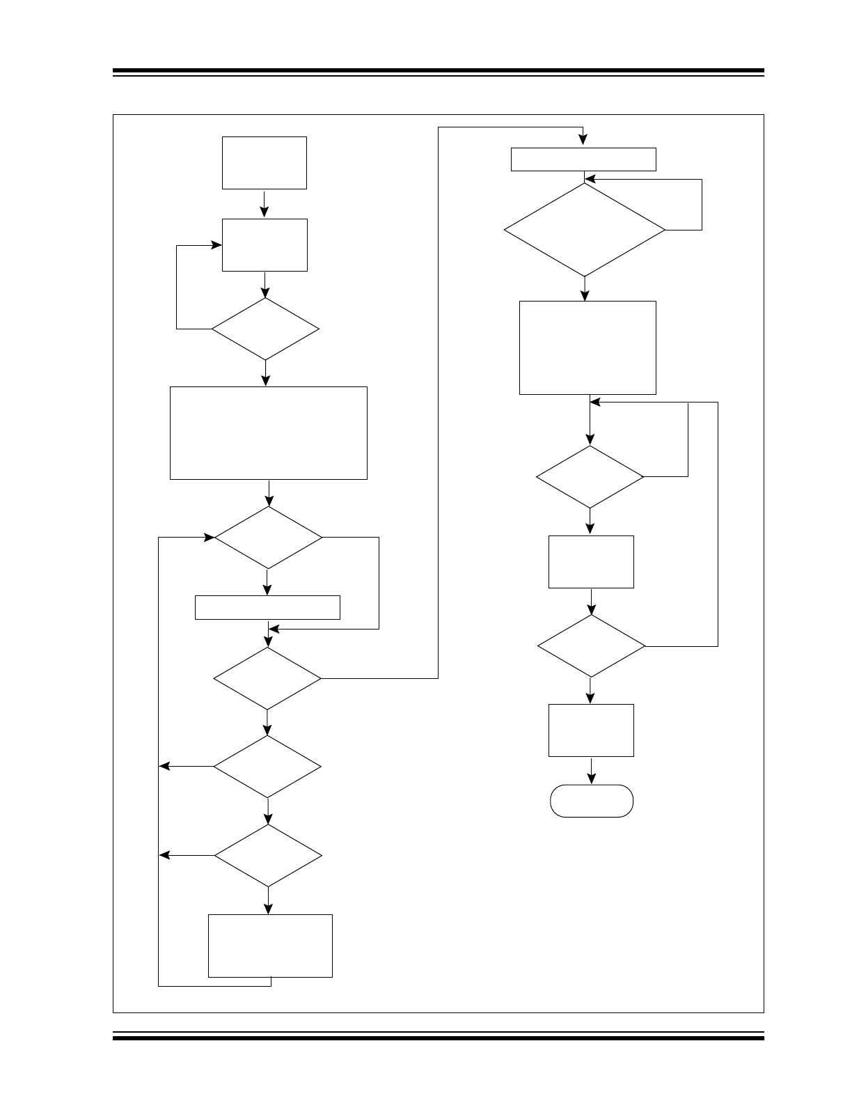
Also refer to Figure 3-5, A/D Operational Flowchart and
the Timing Diagrams, Figure 3-1, Figure 3-2 and
Figure 3-3.
3.1
A/D Converter Operation
When the TC3401 is not converting, it is in Sleep mode
with both the SCLK and SDAT lines high. An A/D
conversion is initiated by a high to low transition on the
SCLK line at which time the internal clock of the
TC3401 is started and the address value (ADDR) is
internally latched. The address value steers the analog
multiplexer to select the input channel to be converted.
Each additional high to low transition of SCLK (follow-
ing the initial SCLK falling edge) during the time interval
t
4,
will decrement the conversion resolution by one bit
and reduce the conversion time by one half. The time
interval t
4
is referred to as the resolution reduction
window. The minimum conversion resolution is 10-bits
so any more than 6 SCLK transitions during t
4
will be
ignored.
After each high to low transition of SCLK, in the t
4
interval, the SDAT output is driven high by the TC3401
to acknowledge that the resolution has been decre-
mented. When the SCLK returns high or the t
4
interval
ends, the SDAT line returns low (see Figure 3-2). When
the conversion is complete SDAT is driven high. The
TC3401 now enters Sleep mode and the conversion
value can be read as a serial data word on the SDAT
line.
3.2
Reading the Data Word
After the conversion is complete and SDAT goes high,
the conversion value can be clocked serially onto the
SDAT line by high to low transitions of the SCLK. The
data word is in two’s compliment format with the sign bit
clocked onto the SDAT line, first followed by the MSB
and ending in the LSB. For a 16-bit conversion the data
word would consist of a sign bit followed by 15 magni-
tude bits, Table 3-1 shows the data word versus input
voltage for a 16-bit conversion. Note that the full scale
input voltage range is ±(2 REF
IN
– 1LSB). When
REF
OUT
is fed back directly to REF
IN
, an LSB is 73
µ
V
for a 16-bit conversion, as REF
OUT
is typically 1.193V.
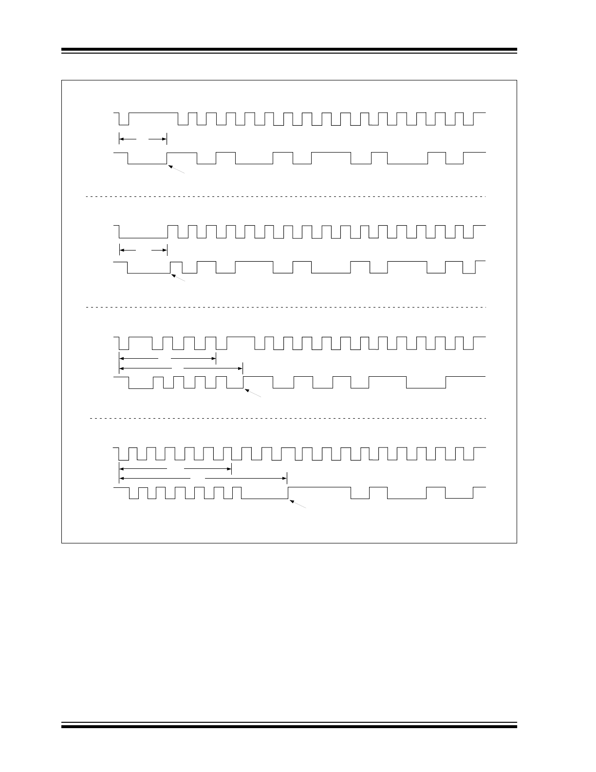
Figure 3-4 shows typical SCLK and SDAT waveforms
for 16, 12 and 10-bit conversions. Note that any com-
plete convert and read cycle requires 17 negative edge
clock pulses. The first is the convert command. Then,
up to six of these can occur in the resolution reduction
window, t
4
, to decrement resolution. The remaining
pulses clock out the conversion data word.
TABLE 3-1:
DATA CONVERSION WORD
VS. VOLTAGE INPUT
(REF
IN
= 1.193V)
The SCLK input has a filter which rejects any positive
or negative pulse of width less than 50nsec to reduce
noise. The rejection width of this pulse can vary
between 50nsec and 750nsec depending on process-
ing parameters and supply voltage.
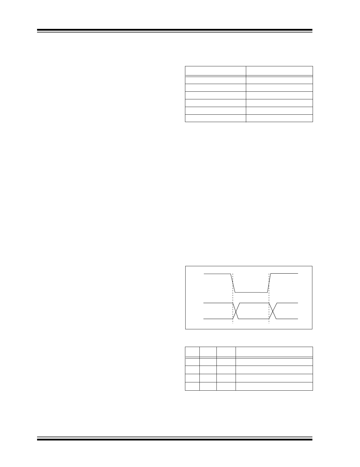
Figure 3-1 and Table 3-2 show information for deter-
mining the mode of operation for the TC3401 part by
recording the value of SDAT for SCLK in a high, then
low, then high state. For example, if SCLK goes
through a 1-0-1 transition and the corresponding
values of SDAT are 1-1-0, then the SCLK falling edge
started a new data conversion. A 0-1-0 for SDAT would
have indicated a resolution reduction had occurred.
This is useful if the microcontroller has a Watchdog
Reset or otherwise loses track of where the TC3401 is
in the conversion and data readout sequence. The
microcontroller can simply transition SCLK until it
“finds” a Start Conversion condition.
FIGURE 3-1:
SCLK, SDAT LOGIC
STATE DIAGRAM
TABLE 3-2:
SCLK, SDAT LOGIC STATE
*
Note: The code X00 has a dual meaning: Data Transfer or
Busy converting. To avoid confusion, the user should
send only the required number of pulses for the
desired resolution, then wait for SDAT to rise to 1,
indicating conversion is complete before clocking
SCLK again to read out data bits.
Data Word
INn+ – INn- (Volts)
0111 1111 1111 1111
2.38596 (Positive Full Scale)
0000 0000 0000 0001
72.8 E -6
0000 0000 0000 0000
0
1111 1111 1111 1111
-72.8 E -6
1000 0000 0000 0001
-2.38596 (Negative Full Scale)
1000 0000 0000 0000
Reserved Code
A
B
C
Status
1
1
0
Start Conversion
0
1
0
Resolution Reduction
x
1
1
Data Transfer
x
0
0
Data Transfer or Busy*
SCLK
SDAT
A
B
C
2002 Microchip Technology Inc.
DS21410B-page 7
TC3401
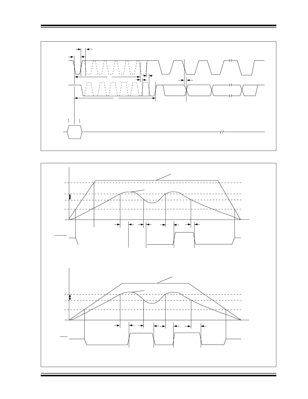
FIGURE 3-2:
CONVERSION AND DATA OUTPUT TIMING
FIGURE 3-3:
RESET AND POWER FAIL TIMING
SCLK
SDAT
t
4
t
1
t
2
t
3
t
8
t
8
D
N-1
D
N-1
D
0
(LSB)
D
N
(MSB)
t
5
Data Conversion
Complete
Sleep
Mode
ADDR
Start Conversion and Resolution Control Timing
Data Output Timing
t
6
t
7
RESET
0
V
TH
1.23
V
DD
Reset Generator Timing
t
9
t
11
Power Fail Comparator Timing
1.1
1.20
Hysteresis
Time
V
olts
PFO
0
PFI
1.23
t
10
t
10
t
10
t
10
1.1
1.20
Hysteresis
Time
V
olts
V
DD
V
DD
t
9
t
11
1.80
TC3401
DS21410B-page 8
2002 Microchip Technology Inc.
FIGURE 3-4:
SCLK AND SDAT WAVEFORMS FOR 16, 12 AND 10-BIT CONVERSIONS
SCLK
SDAT
t
3
a
16-bit Data Conversion,
Data Word A5A5h
SCLK
SDAT
16-bit Data Conversion, Long Start Pulse,
Data Word 5A5Ah
> t
3
a
Data Conversion
Complete
SCLK
SDAT
12-bit Conversion,
Data Word = AB3h
SCLK
SDAT
t
3
g
10-bit Conversion with "Extra"
Data Reduction Clocks, Data Word = 3A4h
Data Conversion
Complete
Data Conversion
Complete
Data Conversion
Complete
t
3
e
< t
4
< t
4
2002 Microchip Technology Inc.
DS21410B-page 9
TC3401
FIGURE 3-5:
A/D OPERATIONAL FLOWCHART
Yes
No
Yes
No
Yes
Yes
Yes
No
No
No
Yes
Yes
No
Yes
No
POR
Sleep
SDAT = High
SCLK
Hgh to Low?
Power Up Analog,
Start CONVCLK (= 0),
Start Conversion,
Resolution = 2m
(m = 16), Latch Input
Channel Address (if applicable).
SCLK
Low to High
transition?
SDAT = Low
CONVCLK
< 2
9
?
SCLK
High to Low?
A/D
Resolution
> 2
10
?
Reduce A/D
Resolution by 1-bit
(m = m – 1);
SDAT = High
SDAT = Low
CONVCLK = 2m?
(Conversion Done?)
Power Down Analog,
Conversion Complete,
SDAT = High
SCLK
High to Low?
SDAT = Dm;
m = m – 1
m
≥ 0?
SDAT = High
Internal Reset
Sleep
No

TC3401
DS21410B-page 10
2002 Microchip Technology Inc.
3.3
V
DD
Monitor
The TC3401 RESET output is in high impedance
provided the voltage at V
TH
is greater than the internal
voltage reference. This reference is approximately the
same value as the voltage appearing at REF
OUT
. When
V
TH
is less than the internal reference, RESET is pulled
low. When V
TH
rises above the internal reference
voltage again, RESET is held low for the reset active
time-out period, t
9
, before being released. The RESET
output is ensured to be valid for V
DD
= 1.3V to 5.5V.
When used to generate a Power-on or Brown-out
Reset, an external resistor network is required to divide
the appropriate V
DD
threshold down to 1.23V at the
V
TH
input, (See the Typical Application circuit). For
example, to generate a POR for a V
DD
at 3V -10%, the
values of R1 and R2 should be 137k
Ω
and 115k
Ω
respectively.
Since RESET is an open drain, it can be wired-OR’ed
with another open drain or external switch if desired.
3.4
Power Fail Detector
The Power Fail detector is a comparator in which the
inverting input is connected to the internal voltage
reference. The non-inverting input is the PFI pin of the
TC3401 and the PFO pin is the active low, open drain
output. This comparator is suitable as an early warning
fail or low battery indicator. In a typical application,
where a voltage regulator is being used to supply
power to a system, the Power Fail comparator would
monitor the input voltage to the regulator while the V
DD
monitor would measure the output voltage of the
regulator. Both PFO and RESET would drive interrupt
pins of a microcontroller.
The Power Fail detector may be used as a Wake-up or
Watchdog Timer. The Typical Application circuit shows
an RC network on PFI with the capacitor tied to a
tristated
µ
C I/O pin. If R4 is 1 M
Ω
and C2 is 10
µ
F, the
time constant is roughly ten seconds. The
µ
C resets
the RC network by driving the I/O tied to PFI low and
then tristating it. The RC network will ramp to 1.23V in
roughly 9 seconds, assuming a V
BATT
of 3.0V. With
PFO tied to a
µ
C input or interrupt, the
µ
C will see a low
to high transition on PFO when the voltage on PFI
exceeds 1.23V. The PFO output is specified to be valid
for V
DD
= 1.3 to 5.5V.