
2017 Microchip Technology Inc.
DS20005785A-page 1
MIC5205
Features
• Ultra-Low Noise Output
• High Output Voltage Accuracy
• Guaranteed 150 mA Output
• Low Quiescent Current
• Low Dropout Voltage
• Extremely Tight Load and Line Regulation
• Very Low Temperature Coefficient
• Current and Thermal Limiting
• Reverse-Battery Protection
• Zero Off-Mode Current
• Logic-Controlled Electronic Enable
Applications
• Cellular Telephones
• Laptop, Notebook, and Palmtop Computers
• Battery-Powered Equipment
• PCMCIA V
CC
and V
PP
Regulation/Switching
• Consumer/Personal Electronics
• SMPS Post-Regulator and DC/DC Modules
• High-Efficiency Linear Power Supplies
General Description
The MIC5205 is an efficient linear voltage regulator
with ultra low-noise output, very low dropout voltage
(typically 17 mV at light loads and 165 mV at 150 mA),
and very low ground current (600 µA at 100 mA
output). The MIC5205 offers better than 1% initial
accuracy.
Designed especially for hand-held, battery-powered
devices, the MIC5205 includes a CMOS or TTL
compatible enable/shutdown control input. When shut
down, power consumption drops nearly to zero.
Regulator ground current increases only slightly in
dropout, further prolonging battery life.
Key MIC5205 features include a reference bypass pin
to improve its already excellent low-noise performance,
reversed-battery protection, current limiting, and
overtemperature shutdown.
The MIC5205 is available in fixed and adjustable output
voltage versions in a small SOT-23-5 package.
For low-dropout regulators that are stable with ceramic
output capacitors, see the µCap MIC5245/6/7 family.
Package Type
MIC5205
5-Lead SOT-23 (M5)
IN
OUT
BYP
EN
LBxx
KBxx
Part
Identification
1
3
4
5
IN
OUT
ADJ
EN
LBAA
KBAA
1
3
4
5
2
2
GND
GND
Pb-Free
Marking
150 mA Low-Noise LDO Regulator
MIC5205
DS20005785A-page 2
2017 Microchip Technology Inc.
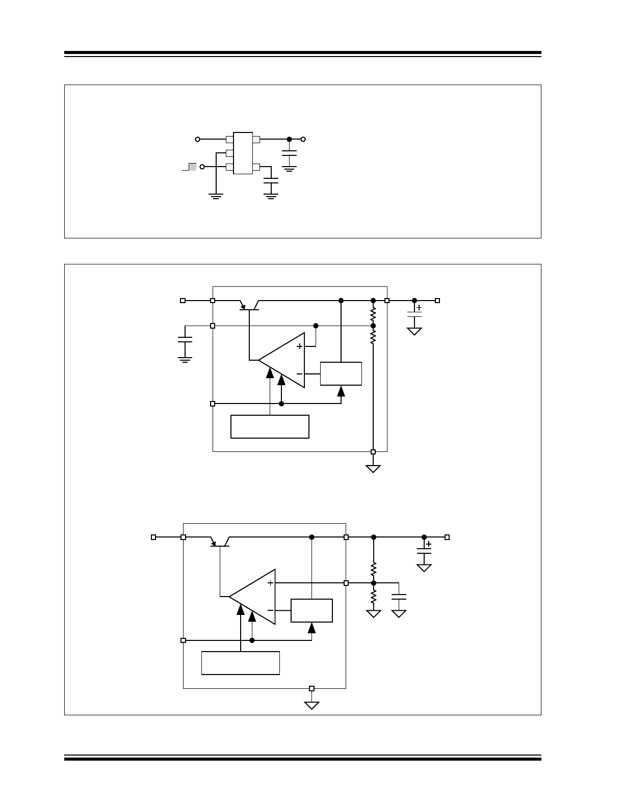
Typical Application Circuit
Functional Block Diagrams
MIC5205
5-Lead SOT-23
1
5
2
3
4
C
OUT
= 2.2μF
tantalum
C
BYP
Enable
Shutdown
EN
V
OUT
Low-Noise Operation:
C
BYP
= 470pF, C
OUT
≥ 2.2μF
Basic Operation:
C
BYP
= not used, C
OUT
≥ 1μF
MIC5205-x.xYM5
EN (pin 3) may be
connected directly
to IN (pin 1).
V
IN
IN
EN
OUT
BYP
C
BYP
(optional)
GND
V
REF
Bandgap
Ref.
Current Limit
Thermal Shutdown
C
OUT
V
OUT
V
IN
MIC5205-x.xYM5
Ultra-Low Noise Fixed Regulator
IN
EN
OUT
C
BYP
(optional)
GND
V
REF
Bandgap
Ref.
Current Limit
Thermal Shutdown
C
OUT
V
OUT
V
IN
R1
R2
MIC5205YM5
ADJ
V
OUT
= V
REF
(1 + R2/R1)
Ultra-Low Noise Adjustable
Regulator
2017 Microchip Technology Inc.
DS20005785A-page 3
MIC5205
1.0
ELECTRICAL CHARACTERISTICS
Absolute Maximum Ratings †
Supply Input Voltage (V
IN
) .......................................................................................................................... –20V to +20V
Enable Input Voltage (V
EN
) ......................................................................................................................... –20V to +20V
Power Dissipation (P
D
) (
Note 1
) ............................................................................................................ Internally Limited
Operating Ratings ‡
Supply Input Voltage (V
IN
) ......................................................................................................................... +2.5V to +16V
Enable Input Voltage (V
EN
) .................................................................................................................................0V to V
IN
† Notice: Stresses above those listed under “Absolute Maximum Ratings” may cause permanent damage to the device.
This is a stress rating only and functional operation of the device at those or any other conditions above those indicated
in the operational sections of this specification is not intended. Exposure to maximum rating conditions for extended
periods may affect device reliability.
‡ Notice: The device is not guaranteed to function outside its operating ratings.
Note 1: The maximum allowable power dissipation at any T
A
(ambient temperature) is P
D(max)
= (T
J(max)
– T
A
)/
JA
.
Exceeding the maximum allowable power dissipation will result in excessive die temperature, and the reg-
ulator will go into thermal shutdown. The
JA
of the MIC5205-xxYM5 (all versions) is 220°C/W mounted on
a PC board.
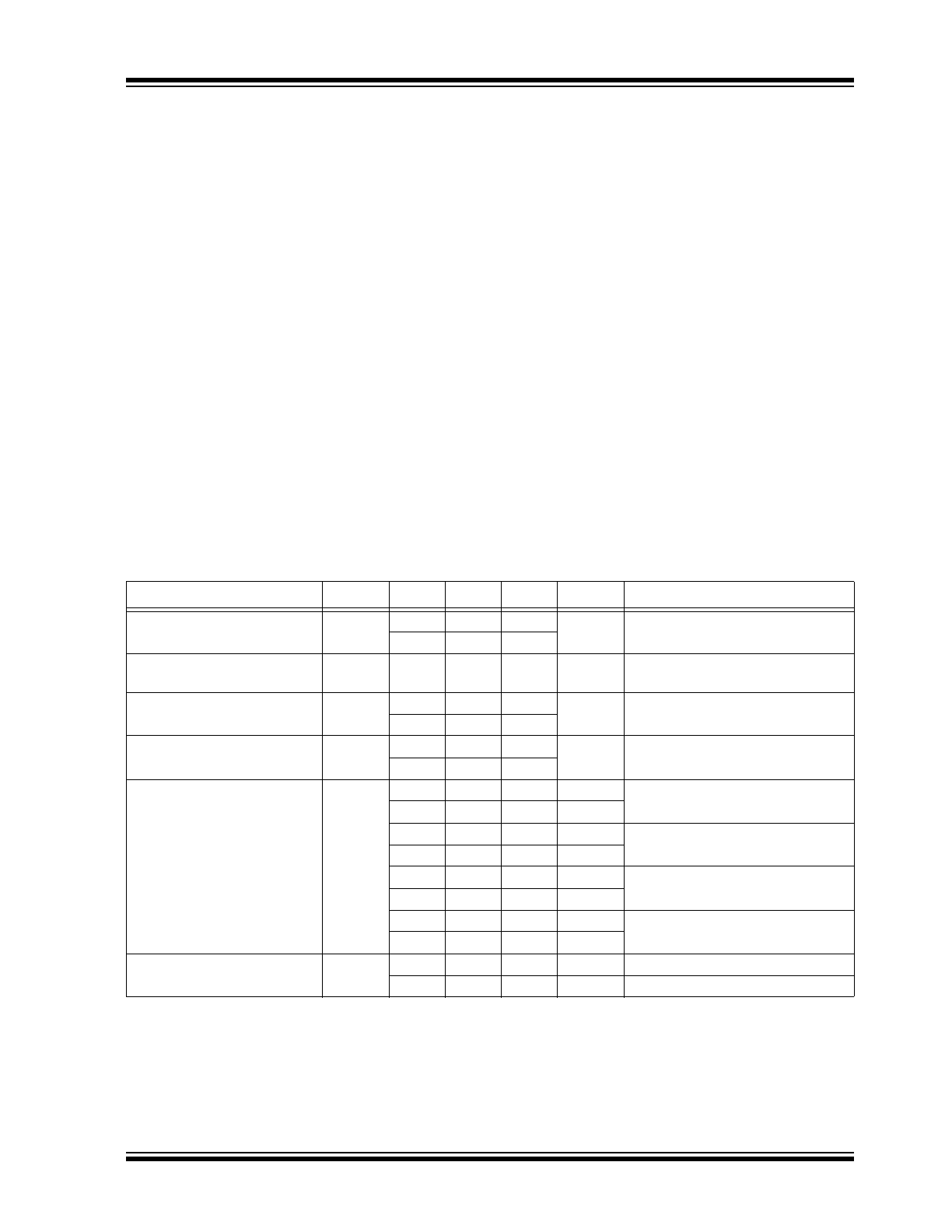
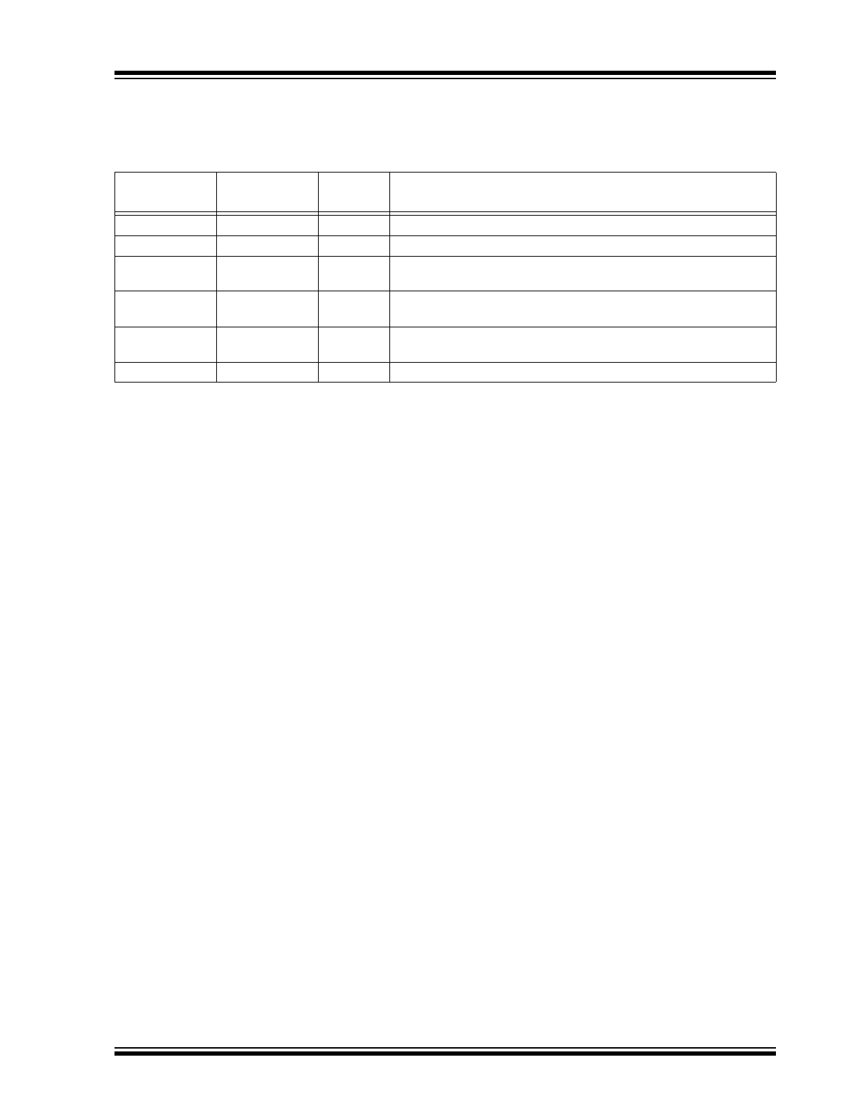
TABLE 1-1:
ELECTRICAL CHARACTERISTICS
Electrical Characteristics: V
IN
= V
OUT
+1V; I
L
= 100 µA; C
L
= 1.0 µF; V
EN
≥ 2.0V; T
J
= +25°C, bold values indicate
–40°C < T
J
< +125°C, unless noted.
Parameter
Symbol
Min.
Typ.
Max.
Units
Conditions
Output Voltage Accuracy
V
O
–1
—
1
%
Variation from specified V
OUT
–2
—
2
Output Voltage Temperature
Coefficient
∆V
O
/∆T
—
40
—
ppm/°C
Note 1
Line Regulation
∆V
O
/V
O
—
0.004
0.012
%/V
V
IN
= V
OUT
+ 1V to 16V
—
—
0.05
Load Regulation
∆V
O
/V
O
—
0.02
0.2
%
I
L
= 0.1 mA to 150 mA,
Note 2
—
—
0.5
Dropout Voltage,
Note 3
V
IN
– V
O
—
10
50
mV
I
L
= 100 µA
—
—
70
mV
—
110
150
mV
I
L
= 50 mA
—
—
230
mV
—
140
250
mV
I
L
= 100 mA
—
—
300
mV
—
165
275
mV
I
L
= 150 mA
—
—
350
mV
Quiescent Current
I
GND
—
0.01
1
µA
V
EN
≤ 0.4V (shutdown)
—
—
5
µA
V
EN
≤ 0.18V (shutdown)
MIC5205
DS20005785A-page 4
2017 Microchip Technology Inc.
Ground Pin Current,
Note 4
I
GND
—
80
125
µA
V
EN
≥ 2.0V, I
L
= 100 µA
—
—
150
µA
—
350
600
µA
I
L
= 50 mA
—
—
800
µA
—
600
1000
µA
I
L
= 100 mA
—
—
1500
µA
—
1300
1900
µA
I
L
= 150 mA
—
—
2500
µA
Ripple Rejection
PSRR
—
75
—
dB
Frequency = 100 Hz, I
L
= 100 µA
Current Limit
I
LIMIT
—
320
500
mA
V
OUT
= 0V
Thermal Regulation
∆V
O
/∆
PD
—
0.05
—
%/W
Note 5
Output Noise
e
NO
—
260
—
nV/√Hz
I
L
= 50 mA, C
L
= 2.2 µF, 470 pF
from BYP to GND
ENABLE Input
Enable Input Logic-Low
Voltage
V
IL
—
—
0.4
V
Regulator shutdown
—
—
0.18
Enable Input Logic-High
Voltage
V
IH
2.0
—
—
V
Regulator enabled
Enable Input Current
I
IL
—
0.01
–1
µA
V
IL
≤ 0.4V
—
—
–2
V
IL
≤ 0.18V
I
IH
2
5
20
V
IL
= 2.0V
—
—
25
V
IL
= 2.0V
Note 1: Output voltage temperature coefficient is defined as the worst case voltage change divided by the total
temperature range.
2: Regulation is measured at constant junction temperature using low duty cycle pulse testing. Parts are
tested for load regulation in the load range from 0.1 mA to 150 mA. Changes in output voltage due to heat-
ing effects are covered by the thermal regulation specification.
3: Dropout Voltage is defined as the input to output differential at which the output voltage drops 2% below its
nominal value measured at 1V differential.
4: Ground pin current is the regulator quiescent current plus pass transistor base current. The total current
drawn from the supply is the sum of the load current plus the ground pin current.
5: Thermal regulation is defined as the change in output voltage at a time “t” after a change in power dissipa-
tion is applied, excluding load or line regulation effects. Specifications are for a 150 mA load pulse at V
IN
=
16V for t = 10 ms.
TABLE 1-1:
ELECTRICAL CHARACTERISTICS (CONTINUED)
Electrical Characteristics: V
IN
= V
OUT
+1V; I
L
= 100 µA; C
L
= 1.0 µF; V
EN
≥ 2.0V; T
J
= +25°C, bold values indicate
–40°C < T
J
< +125°C, unless noted.
Parameter
Symbol
Min.
Typ.
Max.
Units
Conditions
2017 Microchip Technology Inc.
DS20005785A-page 5
MIC5205
TEMPERATURE SPECIFICATIONS (
Note 1
)
Parameters
Sym.
Min.
Typ.
Max.
Units
Conditions
Temperature Ranges
Junction Operating Temperature
Range
T
J
–40
—
+125
°C
—
Storage Temperature Range
T
S
–65
—
+150
°C
—
Lead Temperature
—
—
—
+260
°C
Soldering, 5s
Package Thermal Resistances
Thermal Resistance SOT-23-5
JA
—
220
—
°C/W
Note 2
JC
—
130
—
°C/W
—
Note 1: The maximum allowable power dissipation is a function of ambient temperature, the maximum allowable
junction temperature and the thermal resistance from junction to air (i.e., T
A
, T
J
,
JA
). Exceeding the
maximum allowable power dissipation will cause the device operating junction temperature to exceed the
maximum +125°C rating. Sustained junction temperatures above +125°C can impact the device reliability.
2: The maximum allowable power dissipation at any T
A
(ambient temperature) is P
D(max)
= (T
J(max)
– T
A
)/
JA
.
Exceeding the maximum allowable power dissipation will result in excessive die temperature, and the reg-
ulator will go into thermal shutdown. The
JA
of the MIC5205-xxYM5 (all versions) is 220°C/W mounted on
a PC board.
MIC5205
DS20005785A-page 6
2017 Microchip Technology Inc.
2.0
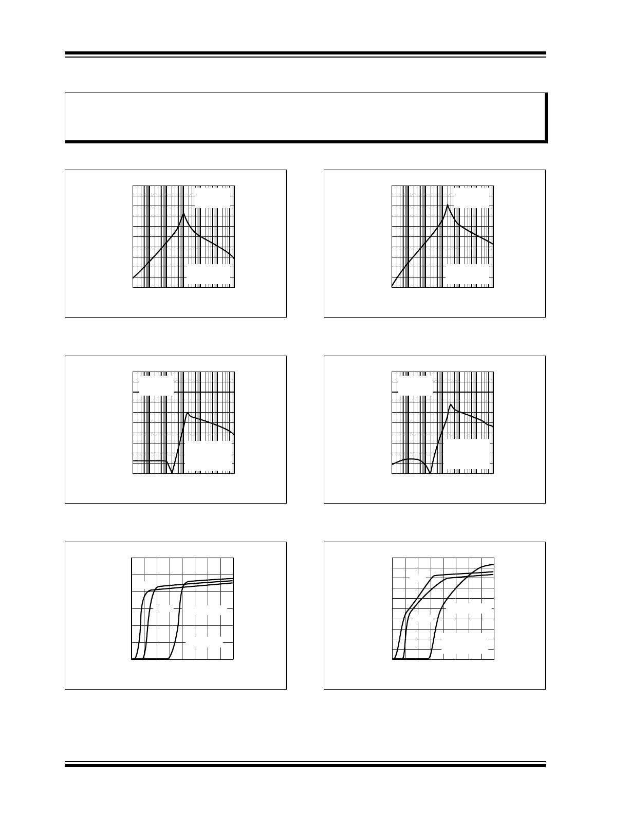
TYPICAL PERFORMANCE CURVES
FIGURE 2-1:
Power Supply Rejection
Ratio.
FIGURE 2-2:
Power Supply Rejection
Ratio.
FIGURE 2-3:
Power Supply Ripple
Rejection vs. Voltage Drop.
FIGURE 2-4:
Power Supply Rejection
Ratio.
FIGURE 2-5:
Power Supply Rejection
Ratio.
FIGURE 2-6:
Power Supply Ripple
Rejection vs. Voltage Drop.
Note:
The graphs and tables provided following this note are a statistical summary based on a limited number of
samples and are provided for informational purposes only. The performance characteristics listed herein
are not tested or guaranteed. In some graphs or tables, the data presented may be outside the specified
operating range (e.g., outside specified power supply range) and therefore outside the warranted range.
-100
-80
-60
-40
-20
0
1E+1 1E+2 1E+3 1E+4 1E+5 1E+6 1E+7
)
B
d(
R
R
S
P
FREQUENCY (Hz)
I
OUT
= 100
μA
C
OUT
= 1
μF
V
IN
= 6V
V
OUT
= 5V
10
100
1k
10k 100k 1M 10M
-100
-80
-60
-40
-20
0
1E+1 1E+2 1E+3 1E+4 1E+5 1E+6 1E+7
)
B
d(
R
R
S
P
FREQUENCY (Hz)
I
OUT
= 100
μA
C
OUT
= 2.2
μF
C
BYP
= 0.01
μF
V
IN
= 6V
V
OUT
= 5V
10
100
1k
10k 100k 1M 10M
0
10
20
30
40
50
60
0
0.1
0.2
0.3
0.4
)
B
d(
N
OI
T
C
E
J
E
R
E
L
P
PI
R
VOLTAGE DROP (V)
I
OUT
= 100mA
10mA
1mA
C
OUT
= 1
μF
-100
-80
-60
-40
-20
0
1E+1 1E+2 1E+3 1E+4 1E+5 1E+6 1E+7
)
B
d(
R
R
S
P
FREQUENCY (Hz)
I
OUT
= 1mA
C
OUT
= 1
μF
V
IN
= 6V
V
OUT
= 5V
10
100
1k
10k 100k 1M 10M
-100
-80
-60
-40
-20
0
1E+1 1E+2 1E+3 1E+4 1E+5 1E+6 1E+7
)
B
d(
R
R
S
P
FREQUENCY (Hz)
I
OUT
= 1mA
C
OUT
= 2.2
μF
C
BYP
= 0.01
μF
V
IN
= 6V
V
OUT
= 5V
10
100
1k
10k 100k 1M 10M
0
10
20
30
40
50
60
70
80
90
100
0
0.1
0.2
0.3
0.4
)
B
d(
N
OI
T
C
E
J
E
R
E
L
P
PI
R
VOLTAGE DROP (V)
I
OUT
= 100mA
10mA
1mA
C
OUT
= 2.2
μF
C
BYP
= 0.01
μF
2017 Microchip Technology Inc.
DS20005785A-page 7
MIC5205
FIGURE 2-7:
Power Supply Rejection
Ratio.
FIGURE 2-8:
Power Supply Rejection
Ratio.
FIGURE 2-9:
Turn-On Time vs. Bypass
Capacitance.
FIGURE 2-10:
Power Supply Rejection
Ratio.
FIGURE 2-11:
Power Supply Rejection
Ratio.
FIGURE 2-12:
Dropout Voltage vs. Output
Current.
-100
-80
-60
-40
-20
0
1E+1 1E+2 1E+3 1E+4 1E+5 1E+6 1E+7
)
B
d(
R
R
S
P
FREQUENCY (Hz)
I
OUT
= 10mA
C
OUT
= 1
μF
V
IN
= 6V
V
OUT
= 5V
10
100
1k
10k 100k 1M 10M
-100
-80
-60
-40
-20
0
1E+1 1E+2 1E+3 1E+4 1E+5 1E+6 1E+7
)
B
d(
R
R
S
P
FREQUENCY (Hz)
I
OUT
= 10mA
C
OUT
= 2.2
μF
C
BYP
= 0.01
μF
V
IN
= 6V
V
OUT
= 5V
10
100
1k
10k 100k 1M 10M
10
100
1000
10000
10
100
1000
10000
(
E
MI
T
μ
)
s
CAPACITANCE (pF)
-100
-80
-60
-40
-20
0
1E+1 1E+2 1E+3 1E+4 1E+5 1E+6 1E+7
)
B
d(
R
R
S
P
FREQUENCY (Hz)
I
OUT
= 100mA
C
OUT
= 1
μF
V
IN
= 6V
V
OUT
= 5V
10
100
1k
10k 100k 1M 10M
-100
-80
-60
-40
-20
0
1E+1 1E+2 1E+3 1E+4 1E+5 1E+6 1E+7
)
B
d(
R
R
S
P
FREQUENCY (Hz)
I
OUT
= 100mA
C
OUT
= 2.2
μF
C
BYP
= 0.01
μF
V
IN
= 6V
V
OUT
= 5V
10
100
1k
10k 100k 1M 10M
0
40
80
120
160
200
240
280
320
0
40
80
120
160
)
V
m(
E
G
A
T
L
O
V
T
U
O
P
O
R
D
OUTPUT CURRENT (mA)
+125
°C
+25
°C
–40
°C
MIC5205
DS20005785A-page 8
2017 Microchip Technology Inc.
FIGURE 2-13:
Noise Performance
.
FIGURE 2-14:
Noise Performance
.
FIGURE 2-15:
Noise Performance.
FIGURE 2-16:
Noise Performance.
FIGURE 2-17:
Noise Performance
.
FIGURE 2-18:
Noise Performance.
0.0001
0.001
0.01
0.1
1
10
1E+1 1E+2 1E+3 1E+4 1E+5 1E+6 1E+7
(
E
SI
O
N
μ
/
V
√
)
z
H
FREQUENCY (Hz)
10
100
1k
10k 100k 1M 10M
1mA
C
OUT
= 1
μF
C
BYP
= 10nF
10mA, C
OUT
= 1
μF
V
OUT
= 5V
0.0001
0.001
0.01
0.1
1
10
1E+1 1E+2 1E+3 1E+4 1E+5 1E+6 1E+7
(
E
SI
O
N
μ
/
V)
z
H
FREQUENCY (Hz)
10mA
1mA
100mA
10
100
1k
10k 100k 1M 10M
V
OUT
= 5V
C
OUT
= 10
μF
electrolytic
√
0.0001
0.001
0.01
0.1
1
10
1E+1 1E+2 1E+3 1E+4 1E+5 1E+6 1E+7
(
E
SI
O
N
μ
/
V
√
)
z
H
FREQUENCY (Hz)
10mA
1mA
100mA
10
100
1k
10k 100k 1M 10M
V
OUT
= 5V
C
OUT
= 22
μF
tantalum
C
BYP
= 10nF
0.0001
0.001
0.01
0.1
1
10
1E+1 1E+2 1E+3 1E+4 1E+5 1E+6 1E+7
(
E
SI
O
N
μ
/
V
√
)
z
H
FREQUENCY (Hz)
10mA
1mA
100mA
10
100
1k
10k 100k 1M 10M
V
OUT
= 5V
C
OUT
= 10
μF
electrolytic
C
BYP
= 100pF
0.0001
0.001
0.01
0.1
1
10
1E+1 1E+2 1E+3 1E+4 1E+5 1E+6 1E+7
(
E
SI
O
N
μ
/
V
√
)
z
H
FREQUENCY (Hz)
10mA
1mA
100mA
10
100
1k
10k 100k 1M 10M
V
OUT
= 5V
C
OUT
= 10
μF
electrolytic
C
BYP
= 1nF
0.0001
0.001
0.01
0.1
1
10
1E+1 1E+2 1E+3 1E+4 1E+5 1E+6 1E+7
(
E
SI
O
N
μ
/
V
√
)
z
H
FREQUENCY (Hz)
10mA
1mA
100mA
10
1k
100
10k 100k 1M 10M
V
OUT
= 5V
C
OUT
= 10
μF
electrolytic
C
BYP
= 10nF
2017 Microchip Technology Inc.
DS20005785A-page 9
MIC5205
3.0
PIN DESCRIPTIONS
The descriptions of the pins are listed in
Table 3-1
.
TABLE 3-1:
PIN FUNCTION TABLE
Pin Number
Fixed Version
Pin Number
Adj. Version
Pin Name
Description
1
1
IN
Supply Input
2
2
GND
Ground
3
3
EN
Enable/Shutdown (Input): CMOS compatible input. Logic-high =
enable, logic-low or open = shutdown
4
—
BYP
Reference Bypass: Connect external 470 pF capacitor to GND to
reduce output noise. May be left open.
—
4
ADJ
Adjust (Input): Adjustable regulator feedback input. Connect to
resistor voltage divider.
5
5
OUT
Regulator Output
MIC5205
DS20005785A-page 10
2017 Microchip Technology Inc.
4.0
APPLICATION INFORMATION
4.1
Enable/Shutdown
Forcing EN (enable/shutdown) high (greater than 2V)
enables the regulator. EN is compatible with CMOS
logic gates.
If the enable/shutdown feature is not required, connect
EN (pin 3) to IN (supply input, pin 1). See
Figure 4-1
.
4.2
Input Capacitor
A 1 µF capacitor should be placed from IN to GND if
there are more than 10 inches of wire between the
input and the AC filter capacitor or if a battery is used
as the input.
4.3
Reference Bypass Capacitor
BYP (reference bypass) is connected to the internal
voltage reference. A 470 pF capacitor (C
BYP
)
connected from BYP to GND quiets this reference,
providing a significant reduction in output noise. C
BYP
reduces the regulator phase margin; when using C
BYP
,
output capacitors of 2.2 µF or greater are generally
required to maintain stability.
The start-up speed of the MIC5205 is inversely
proportional to the size of the reference bypass
capacitor. Applications requiring a slow ramp-up of
output voltage should consider larger values of C
BYP
.
Likewise, if rapid turn-on is necessary, consider
omitting C
BYP
.
If output noise is not a major concern, omit C
BYP
and
leave BYP open.
4.4
Output Capacitor
An output capacitor is required between OUT and GND
to prevent oscillation. The minimum size of the output
capacitor is dependent upon whether a reference
bypass capacitor is used. 1.0 µF minimum is
recommended when C
BYP
is not used (see
Figure 4-2
).
2.2 µF minimum is recommended when C
BYP
is 470 pF
(see
Figure 4-1
). Larger values improve the regulator’s
transient response. The output capacitor value may be
increased without limit.
The output capacitor should have an ESR (effective
series resistance) of about 5Ω or less and a resonant
frequency above 1 MHz. Ultra-low-ESR capacitors can
cause a low amplitude oscillation on the output and/or
underdamped transient response. Most tantalum or
aluminum electrolytic capacitors are adequate; film
types will work, but are more expensive. Because
many aluminum electrolytics have electrolytes that
freeze at about –30°C, solid tantalums are
recommended for operation below –25°C.
At lower values of output current, less output
capacitance is required for output stability. The
capacitor can be reduced to 0.47 µF for current below
10 mA or 0.33 µF for currents below 1 mA.
4.5
No-Load Stability
The MIC5205 will remain stable and in regulation with
no load (other than the internal voltage divider) unlike
many other voltage regulators. This is especially
important in CMOS RAM keep-alive applications.
4.6
Thermal Considerations
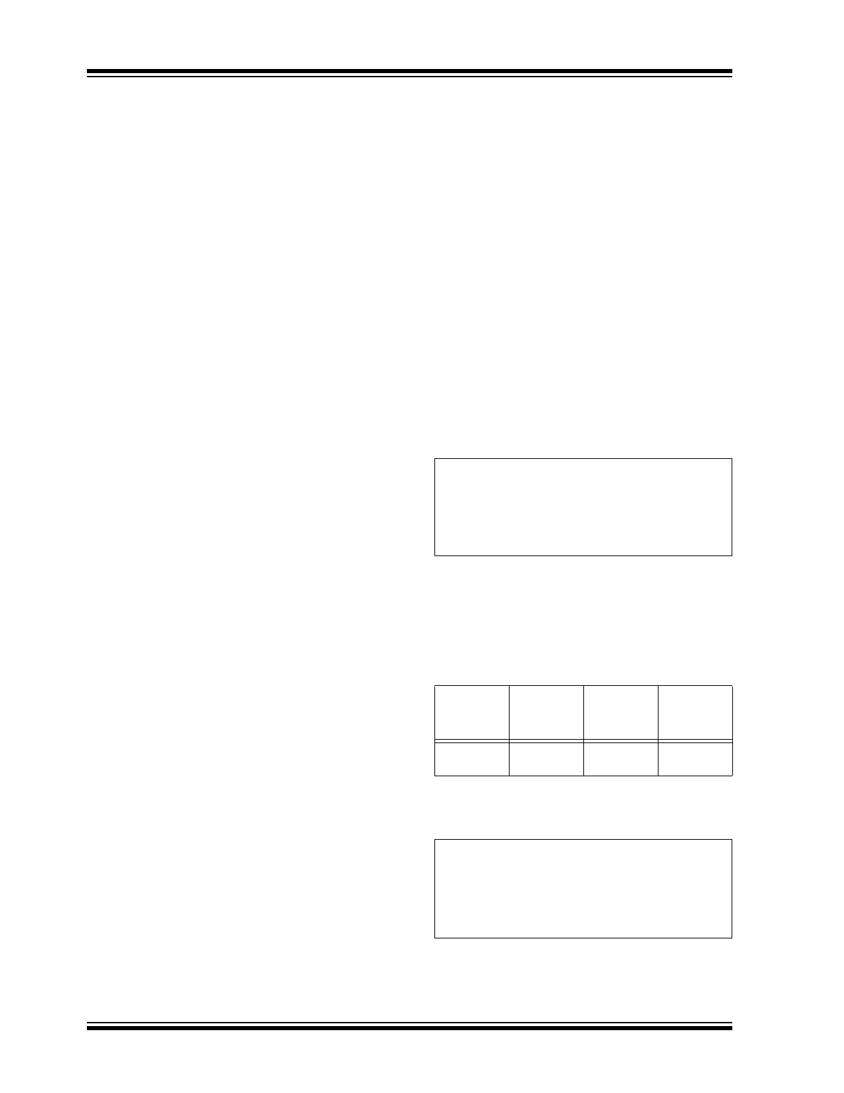
The MIC5205 is designed to provide 150 mA of
continuous current in a very small package. Maximum
power dissipation can be calculated based on the
output current and the voltage drop across the part. To
determine the maximum power dissipation of the
package, use the junction-to-ambient thermal
resistance of the device and the following basic
equation:
EQUATION 4-1:
T
J(MAX)
is the maximum junction temperature of the
die, 125°C, and T
A
is the ambient operating
temperature. θ
JA
is layout dependent;
Table 4-1
shows
examples of junction-to-ambient thermal resistance for
the MIC5205.
The actual power dissipation of the regulator circuit can
be determined using the equation:
EQUATION 4-2:
Substituting P
D(MAX)
for P
D
and solving for the
operating conditions that are critical to the application
will give the maximum operating conditions for the
TABLE 4-1:
SOT-23-5 THERMAL
RESISTANCE
Package
θ
JA
Rec.
Min.
Footprint
θ
JA
Square
Copper
Clad
θ
JC
SOT-23-5
(M5)
220°C/W
170°C/W
130°C/W
P
D MAX
T
J MAX
T
A
–
JA
-------------------------------------
=
P
D
V
IN
V
OUT
–
I
OUT
V
IN
+
I
GND
=