
2010 Microchip Technology Inc.
DS22051D-page 1
MCP1801
Features:
• 150 mA Maximum Output Current
• Low Dropout Voltage, 200 mV typical @ 100 mA
• 25 µA Typical Quiescent Current
• 0.01 µA Typical Shutdown Current
• Input Operating Voltage Range: 2.0V to 10.0V
• Standard Output Voltage Options:
- 0.9V, 1.2V, 1.8V, 2.5V, 3.0V, 3.3V, 5.0V, 6.0V
• Output Voltage Accuracy:
- ±2% (V
R
> 1.5V), ±30 mV (V
R
1.5V)
• Stable with Ceramic Output Capacitors
• Current Limit Protection
• Shutdown Pin
• High PSRR: 70 dB typical @ 10 kHz
Applications:
• Battery-powered Devices
• Battery-powered Alarm Circuits
• Smoke Detectors
• CO
2
Detectors
• Pagers and Cellular Phones
• Wireless Communications Equipment
• Smart Battery Packs
• Low Quiescent Current Voltage Reference
• PDAs
• Digital Cameras
• Microcontroller Power
• Solar-Powered Instruments
• Consumer Products
• Battery Powered Data Loggers
Related Literature:
• AN765, “Using Microchip’s Micropower LDOs”,
DS00765, Microchip Technology Inc., 2002
• AN766, “Pin-Compatible CMOS Upgrades to
BiPolar LDOs”, DS00766,
Microchip Technology Inc., 2002
• AN792, “A Method to Determine How Much
Power a SOT23 Can Dissipate in an Application”,
DS00792, Microchip Technology Inc., 2001
Description:
The MCP1801 is a family of CMOS low dropout (LDO)
voltage regulators that can deliver up to 150 mA of
current while consuming only 25 µA of quiescent
current (typical). The input operating range is specified
from 2.0V to 10.0V, making it an ideal choice for two to
six primary cell battery-powered applications, 9V
alkaline and one or two cell Li-Ion-powered
applications.
The MCP1801 is capable of delivering 100 mA with
only 200 mV (typical) of input to output voltage
differential (V
OUT
= 3.3V). The output voltage tolerance
of the MCP1801 at +25°C is typically ±0.4% with a
maximum of ±2%. Line regulation is ±0.01% typical at
+25°C.
The LDO output is stable with a minimum of 1 µF of
output capacitance. Ceramic, tantalum, or aluminum
electrolytic capacitors can all be used for input and
output. Overcurrent limit with current foldback provides
short-circuit protection. A shutdown (SHDN) function
allows the output to be enabled or disabled. When
disabled, the MCP1801 draws only 0.01 µA of current
(typical).
The MCP1801 is available in a SOT-23-5 package.
Package Types
SOT-23-5
1
2
3
5
4
V
OUT
NC
V
IN
SHDN
V
SS
150 mA, High PSRR, Low Quiescent Current LDO
MCP1801
DS22051D-page 2
2010 Microchip Technology Inc.
Functional Block Diagram
Typical Application Circuit
+
-
MCP1801
V
IN
V
OUT
GND
+V
IN
Error Amplifier
Voltage
Reference
Current Limiter
Shutdown
Control
SHDN
+V
IN
MCP1801
V
IN
C
IN
1 µF
C
OUT
1 µF Ceramic
V
IN
9V
Battery
+
V
OUT
NC
G
ND
SHDN
Ceramic
V
OUT
3.3V @ 40 mA
1
2
3
5
4
2010 Microchip Technology Inc.
DS22051D-page 3
MCP1801
1.0
ELECTRICAL
CHARACTERISTICS
Absolute Maximum Ratings †
Input Voltage ................................................................. +12V
Output Current (Continuous) ..................... P
D
/(V
IN
-V
OUT
)mA
Output Current (Peak) ............................................... 500 mA
Output Voltage ............................... (V
SS
-0.3V) to (V
IN
+0.3V)
SHDN Voltage ..................................(V
SS
-0.3V) to (V
IN
+0.3V)
Continuous Power Dissipation:
SOT-23-5 .............................................................. 250 mW
† Notice: Stresses above those listed under “Maximum
Ratings” may cause permanent damage to the device.
This is a stress rating only and functional operation of
the device at those or any other conditions above those
indicated in the operational listings of this specification
is not implied. Exposure to maximum rating conditions
for extended periods may affect device reliability.
ELECTRICAL CHARACTERISTICS
Electrical Specifications: Unless otherwise specified, all limits are established for V
IN
= V
R
+ 1.0V,
Note 1
, C
OUT
= 1 µF (X7R),
C
IN
= 1 µF (X7R), V
SHDN
= V
IN
, T
A
= +25°C.
Parameters
Sym
Min
Typ
Max
Units
Conditions
Input / Output Characteristics
Input Operating Voltage
V
IN
2.0
—
10.0
V
Note 1
Input Quiescent Current
I
q
—
25
50
µA
I
L
= 0 mA
Shutdown Current
I
SHDN
—
0.01
0.10
µA
SHDN = 0V
Maximum Output Current
I
OUT_mA
150
—
—
mA
Current Limiter
I
LIMIT
—
300
—
mA
if V
R
1.75V, then V
IN
= V
R
+ 2.0V
Output Short Circuit Current
I
OUT_SC
—
50
—
mA
if V
R
1.75V, then V
IN
= V
R
+ 2.0V
Output Voltage Regulation
V
OUT
V
R
-2.0%
V
R
V
R
+2.0%
V
V
R
1.45V, I
OUT
= 30 mA,
Note 2
V
R
-30 mV
V
R
V
R
+30 mV
V
R
1.45V, I
OUT
= 30 mA
V
OUT
Temperature Coeffi-
cient
TCV
OUT
—
100
—
ppm/°C
I
OUT
= 30 mA, -40°C
T
A
+85°C,
Note 3
Line Regulation
V
OUT
/
(V
OUT
X
V
IN
)
-0.2
±0.01
+0.2
%/V
(V
R
+ 1V)
V
IN
10V,
Note 1
V
R
1.75V, I
OUT
= 30 mA
V
R
1.75V, I
OUT
= 10 mA
Load Regulation
V
OUT
/V
OUT
—
15
50
mV
I
L
= 1.0 mA to 100 mA,
Note 4
Dropout Voltage
,
Note 5
V
DROPOUT
—
60
90
mV
I
L
= 30 mA, 3.1V
V
R
6.0V
—
200
250
I
L
= 100 mA, 3.1V
V
R
6.0V
—
80
120
I
L
= 30 mA, 2.0V
V
R
3.1V
—
240
350
I
L
= 100 mA, 2.0V
V
R
< 3.1V
—
2.07 - V
R
2.10 - V
R
V
I
L
= 30 mA, V
R
2.0V
—
2.23 - V
R
2.33 - V
R
I
L
= 100 mA, V
R
< 2.0V
Power Supply Ripple
Rejection Ratio
PSRR
—
70
—
dB
f = 10 kHz, I
L
= 50 mA,
V
INAC
= 1V pk-pk, C
IN
= 0 µF,
if V
R
1.5V, then V
IN
= 2.5V
Output Noise
e
N
—
0.6
—
µV/
Hz
I
OUT
=100 mA, f=1 kHz,
C
OUT
=1 µF (X7R Ceramic),
V
OUT
=3.3V
Note 1:
The minimum V
IN
must meet two conditions: V
IN
2.0V and V
IN
(V
R
+ 1.0V).
2:
V
R
is the nominal regulator output voltage. For example: V
R
= 1.8V, 2.5V, 3.0V, 3.3V, or 5.0V.
The input voltage V
IN
= V
R
+ 1.0V or Vi
IN
= 2.0V (whichever is greater); I
OUT
= 100 µA.
3:
TCV
OUT
= (V
OUT-HIGH
- V
OUT-LOW
) *10
6
/ (V
R
*
Temperature), V
OUT-HIGH
= highest voltage measured over the
temperature range. V
OUT-LOW
= lowest voltage measured over the temperature range.
4:
Load regulation is measured at a constant junction temperature using low duty cycle pulse testing. Changes in output
voltage due to heating effects are determined using thermal regulation specification TCV
OUT
.
5:
Dropout voltage is defined as the input to output differential at which the output voltage drops 2% below its measured
value with an applied input voltage of V
R
+ 1.0V or 2.0V, whichever is greater.
MCP1801
DS22051D-page 4
2010 Microchip Technology Inc.
TEMPERATURE SPECIFICATIONS
Shutdown Input
Logic High Input
V
SHDN-HIGH
1.6
—
—
V
Logic Low Input
V
SHDN-LOW
—
—
0.25
V
ELECTRICAL CHARACTERISTICS (CONTINUED)
Electrical Specifications: Unless otherwise specified, all limits are established for V
IN
= V
R
+ 1.0V,
Note 1
, C
OUT
= 1 µF (X7R),
C
IN
= 1 µF (X7R), V
SHDN
= V
IN
, T
A
= +25°C.
Parameters
Sym
Min
Typ
Max
Units
Conditions
Note 1:
The minimum V
IN
must meet two conditions: V
IN
2.0V and V
IN
(V
R
+ 1.0V).
2:
V
R
is the nominal regulator output voltage. For example: V
R
= 1.8V, 2.5V, 3.0V, 3.3V, or 5.0V.
The input voltage V
IN
= V
R
+ 1.0V or Vi
IN
= 2.0V (whichever is greater); I
OUT
= 100 µA.
3:
TCV
OUT
= (V
OUT-HIGH
- V
OUT-LOW
) *10
6
/ (V
R
*
Temperature), V
OUT-HIGH
= highest voltage measured over the
temperature range. V
OUT-LOW
= lowest voltage measured over the temperature range.
4:
Load regulation is measured at a constant junction temperature using low duty cycle pulse testing. Changes in output
voltage due to heating effects are determined using thermal regulation specification TCV
OUT
.
5:
Dropout voltage is defined as the input to output differential at which the output voltage drops 2% below its measured
value with an applied input voltage of V
R
+ 1.0V or 2.0V, whichever is greater.
Parameters
Sym
Min
Typ
Max
Units
Conditions
Temperature Ranges
Operating Temperature Range
T
A
-40
—
+85
°C
Storage Temperature Range
Tstg
-55
—
+125
°C
Thermal Package Resistance
Thermal Resistance, 5LD SOT-23
JA
JC
—
—
256
81
—
—
°C/W
EIA/JEDEC JESD51-7
FR-4 0.063 4-Layer Board
2010 Microchip Technology Inc.
DS22051D-page 5
MCP1801
2.0
TYPICAL PERFORMANCE CURVES
Note: Unless otherwise indicated: V
R
= 3.3V, C
OUT
= 1 µF Ceramic (X7R), C
IN
= 1 µF Ceramic (X7R), I
L
= 100 µA,
T
A
= +25°C, V
IN
= V
R
+ 1.0V, SOT-23-5.
Note: Junction Temperature (T
J
) is approximated by soaking the device under test to an ambient temperature equal to the desired junction temperature.
The test time is small enough such that the rise in Junction temperature over the Ambient temperature is not significant.
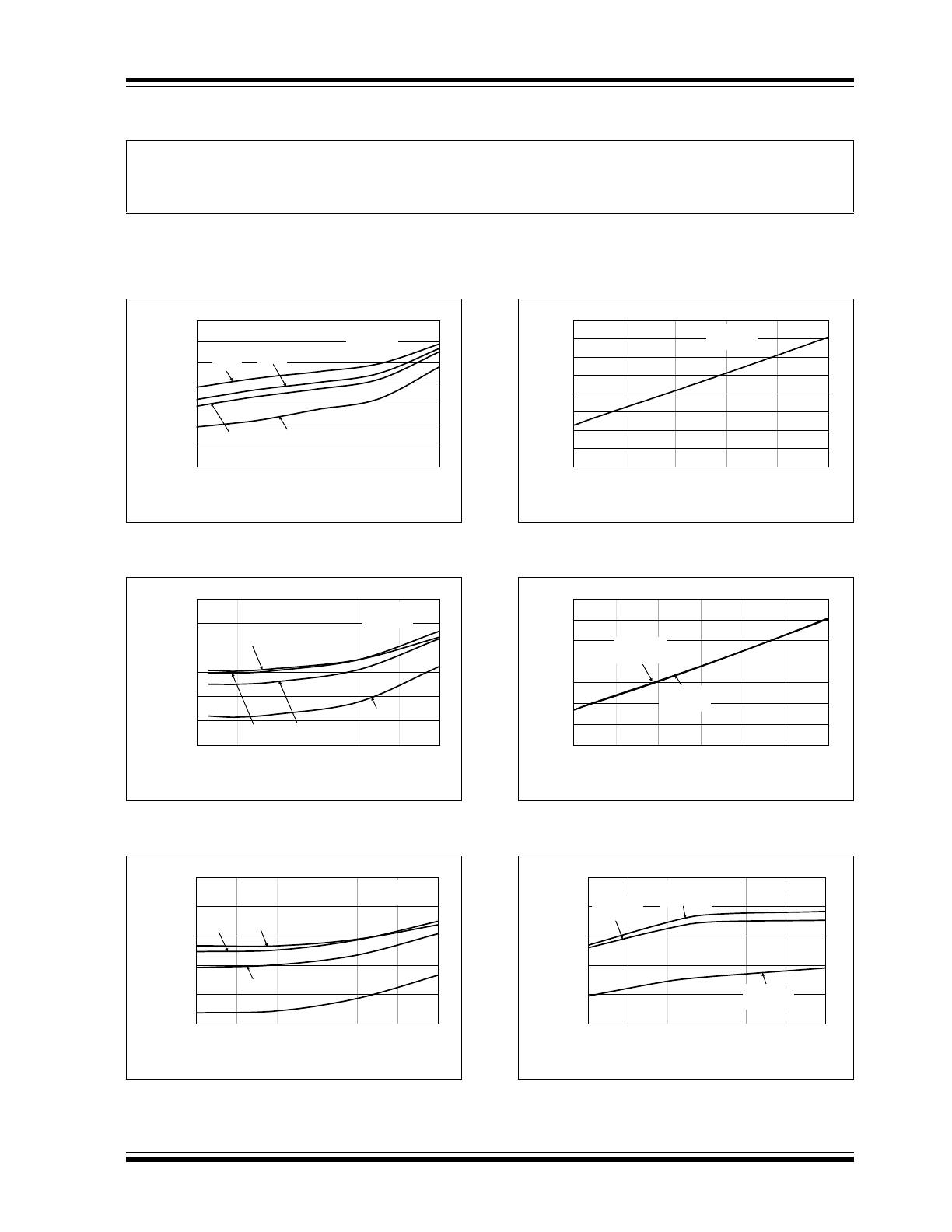
FIGURE 2-1:
Quiescent Current vs. Input
Voltage.
FIGURE 2-2:
Quiescent Current vs. Input
Voltage.
FIGURE 2-3:
Quiescent Current vs. Input
Voltage.
FIGURE 2-4:
Ground Current vs. Load
Current.
FIGURE 2-5:
Ground Current vs. Load
Current.
FIGURE 2-6:
Quiescent Current vs.
Junction Temperature.
Note:
The graphs and tables provided following this note are a statistical summary based on a limited number of
samples and are provided for informational purposes only. The performance characteristics listed herein
are not tested or guaranteed. In some graphs or tables, the data presented may be outside the specified
operating range (e.g., outside specified power supply range) and therefore outside the warranted range.
20.00
21.00
22.00
23.00
24.00
25.00
26.00
27.00
2
4
6
8
10
Input Voltage (V)
Q
u
iesc
ent C
u
rr
e
nt
(
µ
A
)
V
OUT
= 0.9V
I
OUT
= 0 µA
+25°C
-45°C
0°C
+90°C
24.00
25.00
26.00
27.00
28.00
29.00
30.00
4
5
6
7
8
9
10
Input Voltage (V)
Q
u
iesce
nt
C
u
rr
ent (µA
)
V
OUT
= 3.3V
I
OUT
= 0 µA
+25°C
-45°C
0°C
+90°C
25.00
26.00
27.00
28.00
29.00
30.00
7
7.5
8
8.5
9
9.5
10
Input Voltage (V)
Quiesce
nt C
u
rr
en
t (µA
)
V
OUT
= 6.0V
I
OUT
= 0 µA
+25°C
-45°C
0°C
+90°C
0
10
20
30
40
50
60
70
80
0
30
60
90
120
150
Load Current (mA)
G
N
D
C
u
rr
en
t (µA
)
V
OUT
= 0.9V
V
IN
= 2.0V
10
20
30
40
50
60
70
80
0
25
50
75
100
125
150
Load Current (mA)
G
N
D
C
u
rr
en
t (µA
)
V
OUT
= 6.0V
V
IN
= 7.0V
V
OUT
= 3.3V
V
IN
= 4.3V
20.00
22.00
24.00
26.00
28.00
30.00
-45
-22.5
0
22.5
45
67.5
90
Junction Temperature (°C)
Quiesce
nt C
u
rr
en
t (µA
)
I
OUT
= 0 mA
V
OUT
= 0.9V
V
IN
= 2.0V
V
OUT
= 6.0V
V
IN
= 7.0V
V
OUT
= 3.3V
V
IN
= 4.3V
MCP1801
DS22051D-page 6
2010 Microchip Technology Inc.
Note: Unless otherwise indicated: V
R
= 3.3V, C
OUT
= 1 µF Ceramic (X7R), C
IN
= 1 µF Ceramic (X7R), I
L
= 100 µA,
T
A
= +25°C, V
IN
= V
R
+ 1.0V, SOT-23-5.
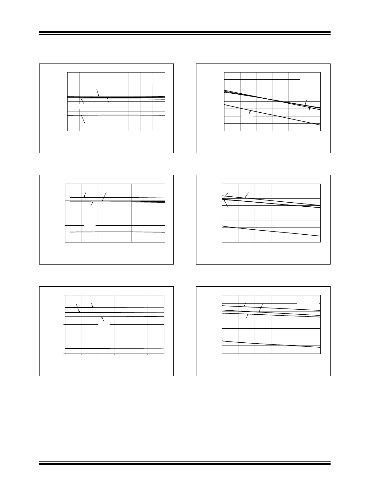
FIGURE 2-7:
Output Voltage vs. Input
Voltage.
FIGURE 2-8:
Output Voltage vs. Input
Voltage.
FIGURE 2-9:
Output Voltage vs. Input
Voltage.
FIGURE 2-10:
Output Voltage vs. Load
Current.
FIGURE 2-11:
Output Voltage vs. Load
Current.
FIGURE 2-12:
Output Voltage vs. Load
Current.
0.890
0.895
0.900
0.905
0.910
0.915
0.920
2
3
4
5
6
7
8
9
10
Input Voltage (V)
O
u
tpu
t V
o
ltage (
V
)
V
OUT
= 0.9V
I
LOAD
= 1 mA
+25°C
-45°C
0°C
+90°C
3.27
3.28
3.29
3.30
3.31
3.32
3.33
3.34
4
5
6
7
8
9
10
Input Voltage (V)
Outp
ut V
o
lt
age (V
)
V
OUT
= 3.3V
I
LOAD
= 1 mA
+25°C
-45°C
0°C
+90°C
5.94
5.96
5.98
6.00
6.02
6.04
6.06
7
7.5
8
8.5
9
9.5
10
Input Voltage (V)
O
u
tp
ut V
o
lta
g
e (V
)
V
OUT
= 6.0V
I
LOAD
= 1 mA
+25°C
-45°C
0°C
+90°C
0.880
0.885
0.890
0.895
0.900
0.905
0.910
0.915
0.920
0
25
50
75
100
125
150
Load Current (mA)
Ou
tpu
t V
o
ltage (V
)
V
IN
= 2.0V
V
OUT
= 0.9V
+25°C, -45°C
0°C
+90°C
3.26
3.27
3.28
3.29
3.30
3.31
3.32
3.33
3.34
0
25
50
75
100
125
150
Load Current (mA)
Outp
ut V
o
lt
age (V
)
V
IN
= 4.3V
V
OUT
= 3.3V
+25°C
-45°C
0°C
+90°C
5.92
5.94
5.96
5.98
6.00
6.02
6.04
6.06
0
25
50
75
100
125
150
Load Current (mA)
Outp
ut V
o
ltag
e (V
)
V
IN
= 7.0V
V
OUT
= 6.0V
+25°C
-45°C
0°C
+90°C
2010 Microchip Technology Inc.
DS22051D-page 7
MCP1801
Note: Unless otherwise indicated: V
R
= 3.3V, C
OUT
= 1 µF Ceramic (X7R), C
IN
= 1 µF Ceramic (X7R), I
L
= 100 µA,
T
A
= +25°C, V
IN
= V
R
+ 1.0V, SOT-23-5.
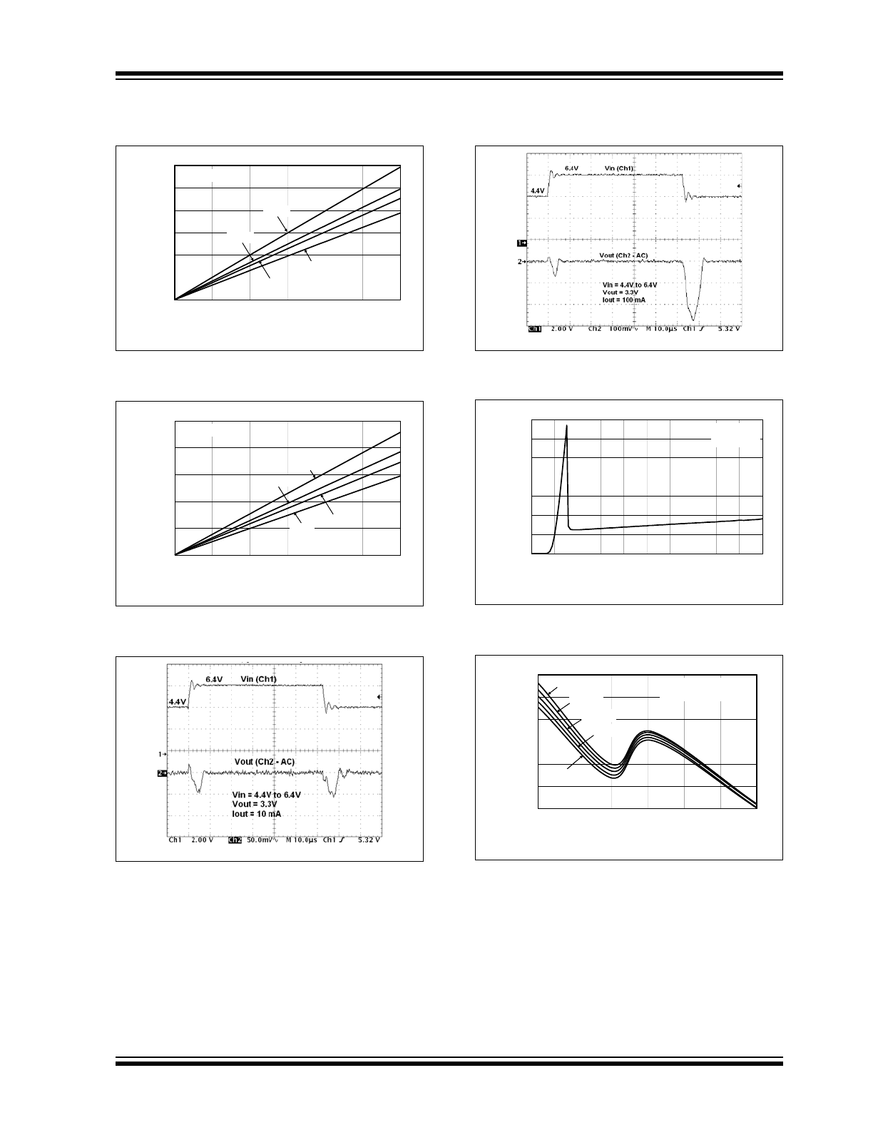
FIGURE 2-13:
Dropout Voltage vs. Load
Current.
FIGURE 2-14:
Dropout Voltage vs. Load
Current.
FIGURE 2-15:
Dynamic Line Response.
FIGURE 2-16:
Dynamic Line Response.
FIGURE 2-17:
Short Circuit Current vs.
Input Voltage.
FIGURE 2-18:
Load Regulation vs.
Temperature.
0.00
0.05
0.10
0.15
0.20
0.25
0.30
0
25
50
75
100
125
150
Load Current (mA)
D
rop
ou
t Vo
ltage (V
)
V
OUT
= 3.3V
+25°C
+0°C
-45°C
+90°C
0.00
0.05
0.10
0.15
0.20
0.25
0
25
50
75
100
125
150
Load Current (mA)
D
ropo
ut V
o
lta
g
e (V
)
V
OUT
= 6.0V
+25°C
+0°C
-45°C
+90°C
0
20
40
60
80
100
120
140
0
1
2
3
4
5
6
7
8
9
10
Input Voltage (V)
S
h
o
rt C
ir
cuit C
u
rre
nt (m
A
)
V
OUT
= 3.3V
R
OUT
< 0.1Ω
-1.60
-1.50
-1.40
-1.30
-1.20
-1.10
-1.00
-45
-22.5
0
22.5
45
67.5
90
Temperature (°C)
Load R
e
gul
at
ion
(%
)
V
OUT
= 0.9V
I
OUT
= 0.1 mA to 150 mA
V
IN
= 6V
V
IN
= 4V
V
IN
= 10V
V
IN
= 8V
V
IN
= 2V
MCP1801
DS22051D-page 8
2010 Microchip Technology Inc.
Note: Unless otherwise indicated: V
R
= 3.3V, C
OUT
= 1 µF Ceramic (X7R), C
IN
= 1 µF Ceramic (X7R), I
L
= 100 µA,
T
A
= +25°C, V
IN
= V
R
+ 1.0V, SOT-23-5.
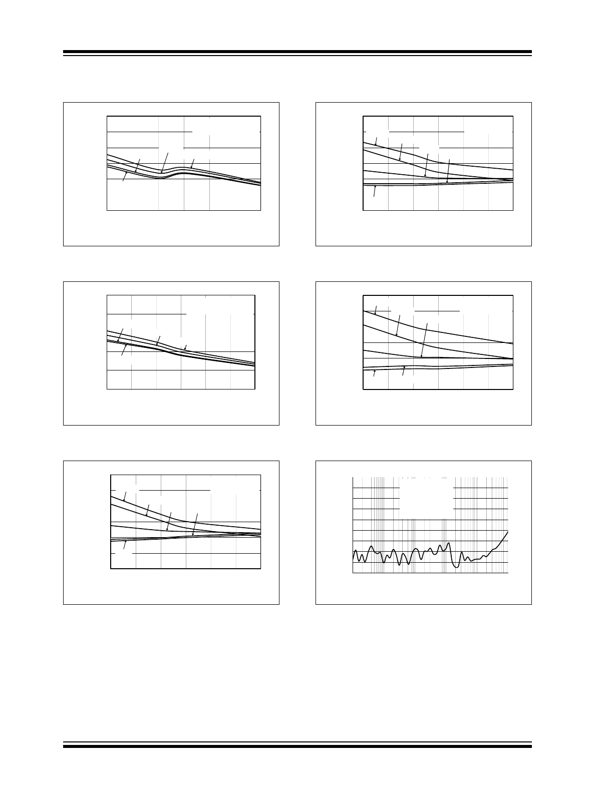
FIGURE 2-19:
Load Regulation vs.
Temperature.
FIGURE 2-20:
Load Regulation vs.
Temperature.
FIGURE 2-21:
Line Regulation vs.
Temperature.
FIGURE 2-22:
Line Regulation vs.
Temperature.
FIGURE 2-23:
Line Regulation vs.
Temperature.
FIGURE 2-24:
PSRR vs. Frequency.
-0.60
-0.50
-0.40
-0.30
-0.20
-0.10
0.00
-45
-22.5
0
22.5
45
67.5
90
Temperature (°C)
Loa
d R
egu
lation (
%
)
V
OUT
= 3.3V
I
OUT
= 0.1 mA to 150 mA
V
IN
= 4.3V
V
IN
= 10V
V
IN
= 8V
V
IN
= 6V
-0.40
-0.30
-0.20
-0.10
0.00
0.10
-45
-22.5
0
22.5
45
67.5
90
Temperature (°C)
L
o
ad
R
egu
la
tion
(
%
)
V
OUT
= 6.0V
I
OUT
= 0.1 mA to 150 mA
V
IN
= 9V
V
IN
= 10V
V
IN
= 7V
V
IN
= 8V
-0.010
-0.005
0.000
0.005
0.010
0.015
0.020
-45
-22.5
0
22.5
45
67.5
90
Temperature (°C)
Lin
e R
egu
la
tion
(
%
/V
)
V
IN
= 2.0 to 10.0V
V
OUT
= 0.9V
10 mA
1 mA
50 mA
100 mA
150 mA
-0.010
-0.005
0.000
0.005
0.010
0.015
0.020
-45
-22.5
0
22.5
45
67.5
90
Temperature (°C)
Line R
eg
u
lation
(%/V
)
V
OUT
= 3.3V
V
IN
= 4.3V to 10V
1 mA
100 mA
10 mA
150 mA
50 mA
-0.010
-0.005
0.000
0.005
0.010
0.015
0.020
-45
-22.5
0
22.5
45
67.5
90
Temperature (°C)
Lin
e R
egu
la
tion
(
%
/V
)
V
OUT
= 6.0V
V
IN
= 7.0V to 10.0V
100 mA
150 mA
1 mA
50 mA
10 mA
-90
-80
-70
-60
-50
-40
-30
-20
-10
0
0.01
0.1
1
10
100
1000
Frequency (kHz)
PS
R
R
(d
B)
V
R
= 3.3V
V
IN
= 4.3V
V
INAC
= 100 mV p-p
C
IN
= 0 μF
I
OUT
= 100 µA
2010 Microchip Technology Inc.
DS22051D-page 9
MCP1801
Note: Unless otherwise indicated: V
R
= 3.3V, C
OUT
= 1 µF Ceramic (X7R), C
IN
= 1 µF Ceramic (X7R), I
L
= 100 µA,
T
A
= +25°C, V
IN
= V
R
+ 1.0V, SOT-23-5.
FIGURE 2-25:
PSRR vs. Frequency.
FIGURE 2-26:
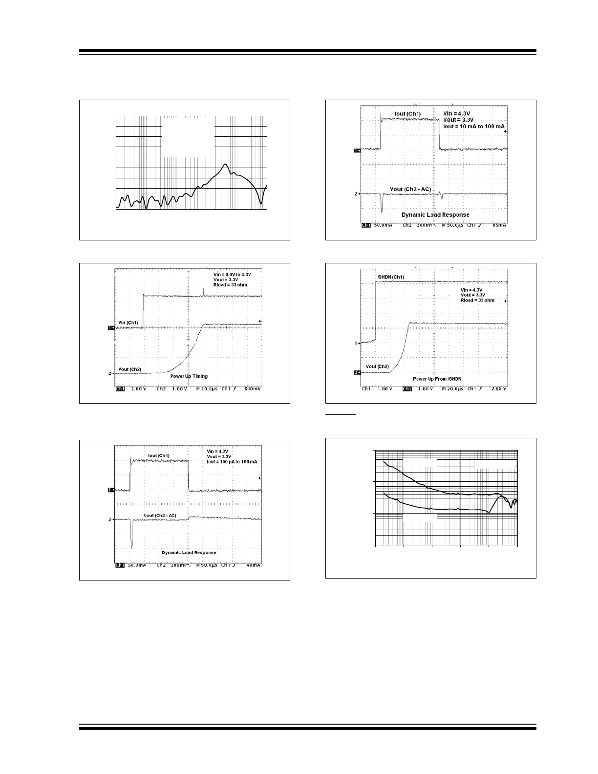
Power-Up Timing.
FIGURE 2-27:
Dynamic Load Response.
FIGURE 2-28:
Dynamic Load Response.
FIGURE 2-29:
Power-Up Timing From
SHDN.
FIGURE 2-30:
Output Noise
-90
-80
-70
-60
-50
-40
-30
-20
-10
0
0.01
0.1
1
10
100
1000
Frequency (kHz)
PSRR (
d
B)
V
R
= 6.0V
V
IN
= 7.0V
V
INAC
= 100 mV p-p
C
IN
= 0 μF
I
OUT
= 100 µA
0.010
0.100
1.000
10.000
0.01
0.1
1
10
100
1000
Frequency (KHz)
Noi
se (µV
/
Hz
)
Vout = 3.3V
Vout = 0.9V
I
OUT
= 100 mA

MCP1801
DS22051D-page 10
2010 Microchip Technology Inc.
NOTES: