
2016 Microchip Technology Inc.
DS20005658A-page 1
MIC24051
Features
• Hyper Speed Control
®
Architecture Enables:
- High Delta V Operation (V
IN
= 19V and V
OUT
= 0.8V)
- Small Output Capacitance
• 4.5V to 19V Voltage Input
• 6A Output Current Capability, up to 95%
Efficiency
• Adjustable Output from 0.8V to 5.5V
• ±1% Feedback Accuracy
• Any Capacitor Stable - Zero-to-High ESR
• 600 kHz Switching Frequency
• No External Compensation
• Power Good (PG) Output
• Foldback Current-Limit and “Hiccup Mode”
Short-Circuit Protection
• Supports Safe Start-Up into a Pre-Biased Load
• –40°C to +125°C Junction Temperature Range
• Available in a 28-pin 5 mm x 6 mm QFN Package
Applications
• Servers and Workstations
• Routers, Switches, and Telecom Equipment
• Base Stations
General Description
The MIC24051 is a constant-frequency, synchronous
buck regulator featuring a unique adaptive on-time
control architecture. The MIC24051 operates over an
input supply range of 4.5V to 19V and provides a
regulated output of up to 6A of output current. The
output voltage is adjustable down to 0.8V with a
guaranteed accuracy of ±1%, and the device operates
at a switching frequency of 600 kHz.
Microchip’s Hyper Speed Control
®
architecture allows
for ultra-fast transient response while reducing the
output capacitance and also makes (High V
IN
)/(Low
V
OUT
) operation possible. This adaptive t
ON
ripple
control architecture combines the advantages of
fixed-frequency operation and fast transient response
in a single device.
The MIC24051 offers a full suite of protection features
to ensure protection of the IC during fault conditions.
These include undervoltage lockout to ensure proper
operation under power-sag conditions, internal
soft-start to reduce inrush current, foldback current
limit, “hiccup mode” short-circuit protection and thermal
shutdown. An open-drain Power Good (PG) pin is
provided.
The 6A HyperLight Load
®
part, MIC24052, is also
available on Microchip’s web site.
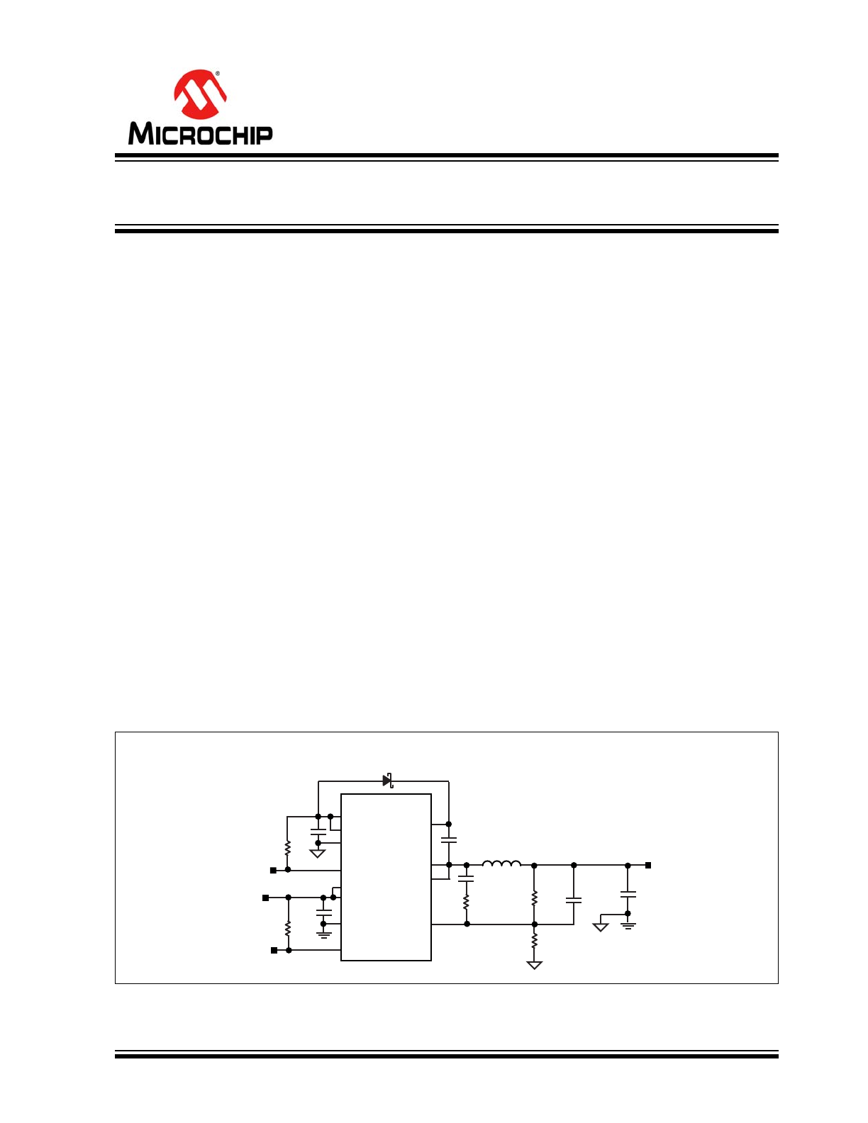
Typical Application Schematic
MIC24051
28-P
IN
QFN
10k
2.2μF
PG
V
IN
4.5V TO 19V
4.7μF
x2
EN
0.1μF
2.2μH
0.1μF
19.6k
2.49k
4.7nF
2.00k
V
OUT
1.8V/6A
100μF
MIC24051
VDD
SGND
PG
VIN
PVIN
PGND
EN
BST
SW
CS
FB
10k
PVDD
12V, 6A High-Efficiency Buck Regulator
with Hyper Speed Control
®
MIC24051
DS20005658A-page 2
2016 Microchip Technology Inc.
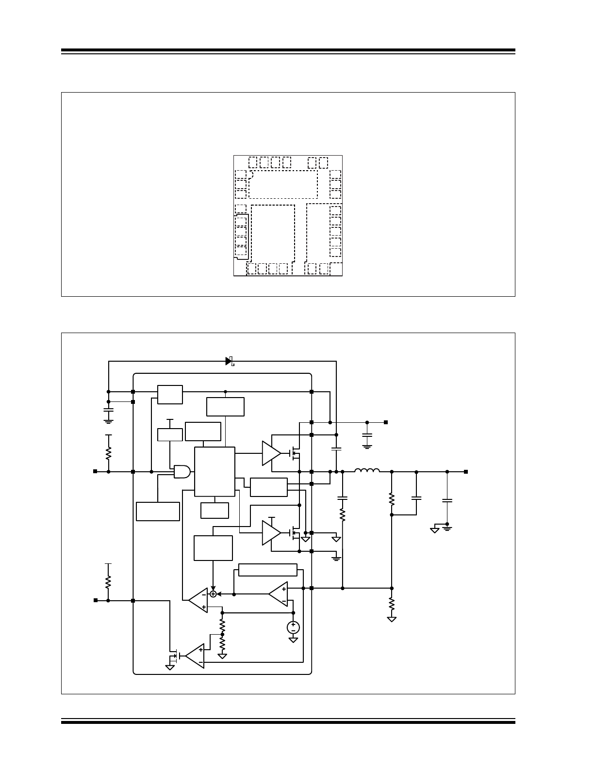
Package Type
Block Diagram
MIC24051
28-Pin QFN (JL)
(Top View)
PVIN
SW
SW
SW
SW
PVIN
1
2
3
4
5
6
7
8
9 10 11 12
13 14
15
16
24
23
22
21
20
19
18
17
28 27 26 25
CS
PGND
BST
PVIN
PVIN
PVIN
PVIN
PVIN
PVDD
PGND
NC
SW
PGND
PGND
PGND
PGND
FB
PG
EN
VIN
VDD
SGND
PGND
SW
PVIN
R1
2.49k
R2
2.00k
0.1μF
19.6k
2.2μF
V
OUT
1.8V/6A
2.2μH
100μF
MIC24051
4.7nF
0.1μF
C
BST
BST
SW
FB
VDD
EN
PGND
VIN
PVIN
V
IN
4.5V to 19V
4.7μF
x2
g
m
EA
COMP
CS
CL and ZC
DETECTION
CONTROL
LOGIC
TIMER
SOFT-START
FIXED T
ON
ESTIMATE
UVLO
LDO
THERMAL
SHUTDOWN
SOFT
START
PVDD
V
REF
0.8V
COMPENSATION
SGND
D1
MODIFIED
T
OFF
PG
10k
VDD
VDD
8%
92%
10k
V
IN
HSD
LSD
INTERNAL
RIPPLE
INJECTION
PVDD

2016 Microchip Technology Inc.
DS20005658A-page 3
MIC24051
1.0
ELECTRICAL CHARACTERISTICS
Absolute Maximum Ratings †
PV
IN
to PGND ............................................................................................................................................ –0.3V to +29V
V
IN
to PGND ............................................................................................................................................... –0.3V to PV
IN
PV
DD
, V
DD
to PGND .................................................................................................................................... –0.3V to +6V
V
SW
, V
CS
to PGND ....................................................................................................................... –0.3V to (PV
IN
+ 0.3V)
V
BST
to V
SW
................................................................................................................................................. –0.3V to +6V
V
BST
to PGND............................................................................................................................................ –0.3V to +35V
V
FB
, V
PG
to PGND ......................................................................................................................... –0.3V to (V
DD
+ 0.3V)
V
EN
to PGND ...................................................................................................................................–0.3V to (V
IN
+ 0.3V)
PGND to SGND ........................................................................................................................................ –0.3V to +0.3V
ESD Rating (
Note 1
) .................................................................................................................................. ESD Sensitive
Operating Ratings ‡
Supply Voltage (PV
IN
, V
IN
)......................................................................................................................... +4.5V to +19V
PV
DD
, V
DD
Supply Voltage (PV
DD
, V
DD
)................................................................................................... +4.5V to +5.5V
Enable Input (V
EN
) ..............................................................................................................................................0V to V
IN
†
Notice: Stresses above those listed under “Absolute Maximum Ratings” may cause permanent damage to the device.
This is a stress rating only and functional operation of the device at those or any other conditions above those indicated
in the operational sections of this specification is not intended. Exposure to maximum rating conditions for extended
periods may affect device reliability.
‡ Notice:
The device is not guaranteed to function outside its operating ratings.
Note 1:
Devices are ESD sensitive. Handling precautions recommended. Human body model, 1.5 kΩ in series with
100 pF.
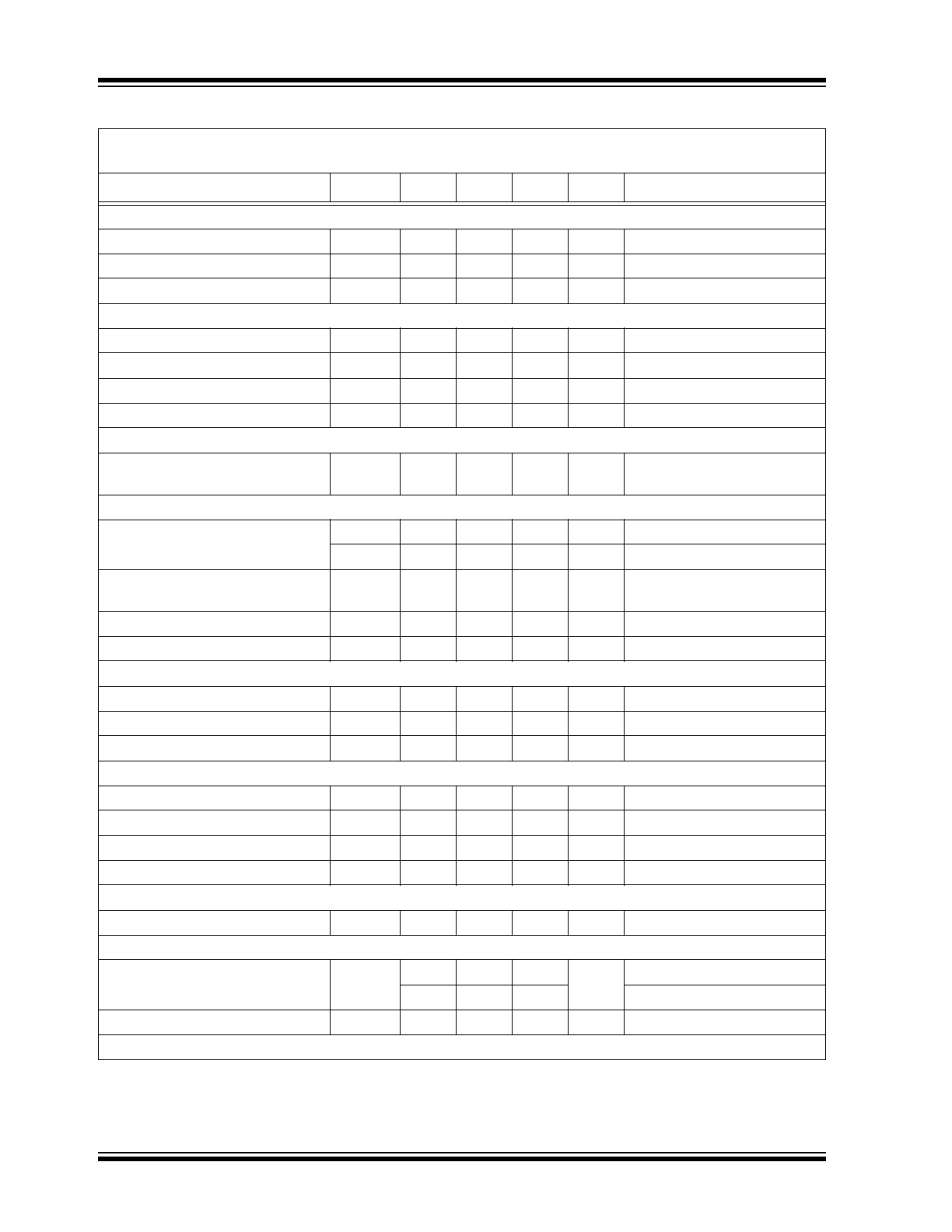
MIC24051
DS20005658A-page 4
2016 Microchip Technology Inc.
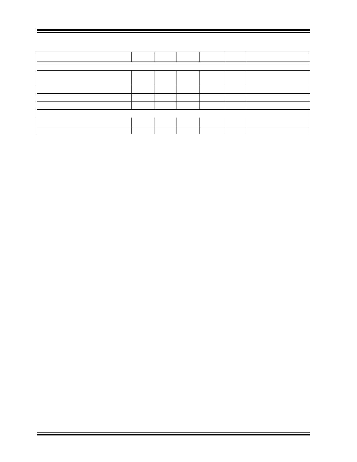
TABLE 1-1:
ELECTRICAL CHARACTERISTICS
Electrical Characteristics:
PV
IN
= V
IN
= V
EN
= 12V, V
BST
– V
SW
= 5V; T
A
= 25°C, unless noted. Bold values
indicate –40°C ≤ T
J
≤ +125°C. (
Note 1
)
.
Parameters
Sym.
Min.
Typ.
Max.
Units
Conditions
Power Supply Input
Input Voltage Range (V
IN
, PV
IN
)
—
4.5
—
19
V
—
Quiescent Supply Current
—
—
730
1500
µA
V
FB
= 1.5V (non-switching)
Shutdown Supply Current
—
—
5
10
µA
V
EN
= 0V
V
DD
Supply Voltage
V
DD
Output Voltage
—
4.8
5
5.4
V
V
IN
= 7V to 19V, I
DD
= 40 mA
V
DD
UVLO Threshold
—
3.7
4.2
4.5
V
V
DD
Rising
V
DD
UVLO Hysteresis
—
400
mV
—
Dropout Voltage (V
IN
– V
DD
)
—
380
600
mV
I
DD
= 25 mA
DC/DC Controller
Output-Voltage Adjust Range
(V
OUT
)
—
0.8
—
5.5
V
—
Reference
Feedback Reference Voltage
—
0.792
0.8
0.808
V
0°C ≤ T
J
≤ +85°C (±1.0%)
—
0.788
0.8
0.812
V
–40°C ≤ T
J
≤ +125°C (±1.5%)
Load Regulation
—
—
0.25
—
%
I
OUT
= 0A to 6A (Continuous
Mode)
Line Regulation
—
—
0.25
—
%
V
IN
= 4.5V to 19V
FB Bias Current
—
—
50
500
nA
V
FB
= 0.8V
Enable Control
EN Logic Level High
—
1.8
—
—
V
—
EN Logic Level Low
—
—
—
0.6
V
—
EN Bias Current
—
—
6
30
µA
V
EN
= 12V
Oscillator
Switching Frequency (
Note 2
)
—
450
600
750
kHz
V
OUT
= 2.5V
Maximum Duty Cycle (
Note 3
)
—
—
82
—
%
V
FB
= 0V
Minimum Duty Cycle
—
—
0
—
%
V
FB
= 1.0V
Minimum Off-Time
—
—
300
—
ns
—
Soft-Start
Soft-Start Time
—
—
3
—
ms
—
Short-Circuit Protection
Peak Inductor Current-Limit
Threshold
—
7.5
11
17
A
V
FB
= 0.8V, T
J
= 25°C
6.6
11
17
V
FB
= 0.8V, T
J
= 125°C
Short-Circuit Current
—
—
8
—
A
V
FB
= 0V
Internal FETs
Note 1:
Specification for packaged product only.
2:
Measured in test mode.
3:
The maximum duty-cycle is limited by the fixed mandatory off-time (t
OFF
) of typically 300 ns.
2016 Microchip Technology Inc.
DS20005658A-page 5
MIC24051
Top MOSFET R
DS(ON)
—
—
42
—
mΩ
I
SW
= 1A
Bottom MOSFET R
DS(ON)
—
—
12.5
—
mΩ
I
SW
= 1A
SW Leakage Current
—
—
—
60
µA
V
EN
= 0V
V
IN
Leakage Current
—
—
—
25
µA
V
EN
= 0V
Power Good (PG)
PG Threshold Voltage
—
85
92
95
%V
OUT
Sweep V
FB
from Low to High
PG Hysteresis
—
—
5.5
—
%V
OUT
Sweep V
FB
from High to Low
PG Delay Time
—
—
100
—
µs
Sweep V
FB
from Low to High
PG Low Voltage
—
—
70
200
mV
Sweep V
FB
< 0.9 x V
NOM
,
I
PG
= 1 mA
Thermal Protection
Overtemperature Shutdown
—
—
160
—
°C
T
J
Rising
Overtemperature Shutdown
Hysteresis
—
—
15
—
°C
—
TABLE 1-1:
ELECTRICAL CHARACTERISTICS (CONTINUED)
Electrical Characteristics:
PV
IN
= V
IN
= V
EN
= 12V, V
BST
– V
SW
= 5V; T
A
= 25°C, unless noted. Bold values
indicate –40°C ≤ T
J
≤ +125°C. (
Note 1
)
.
Parameters
Sym.
Min.
Typ.
Max.
Units
Conditions
Note 1:
Specification for packaged product only.
2:
Measured in test mode.
3:
The maximum duty-cycle is limited by the fixed mandatory off-time (t
OFF
) of typically 300 ns.
MIC24051
DS20005658A-page 6
2016 Microchip Technology Inc.
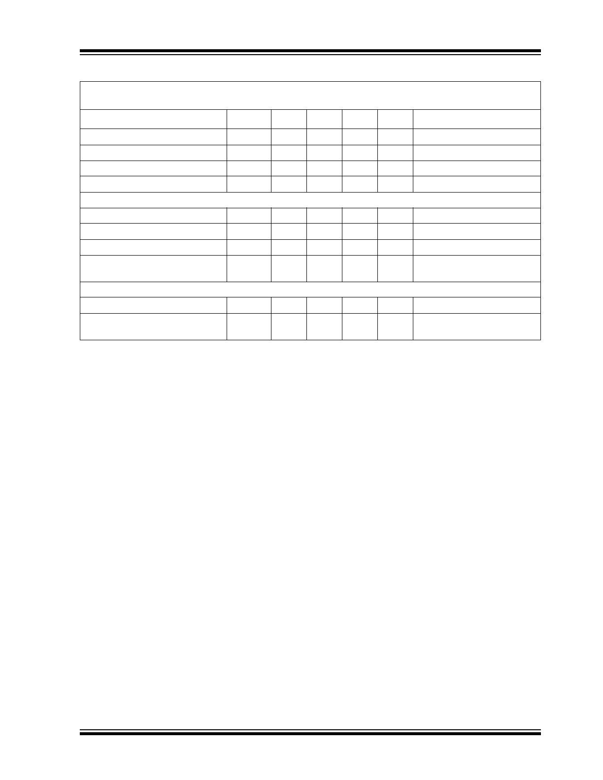
TEMPERATURE SPECIFICATIONS
Parameters
Sym.
Min.
Typ.
Max.
Units
Conditions
Temperature Ranges
Junction Operating Temperature
Range
T
J
–40
—
+125
°C
Note 1
Maximum Junction Temperature
—
—
—
+150
°C
—
Storage Temperature
T
S
–65
—
+150
°C
—
Lead Temperature
—
—
—
+260
°C
Soldering, 10s
Package Thermal Resistances
Thermal Resistance, 5x6 QFN-28
JA
—
28
—
°C/W
Note 2
Thermal Resistance, 5x6 QFN-28
JC
—
2.5
—
°C/W
—
Note 1:
The maximum allowable power dissipation is a function of ambient temperature, the maximum allowable
junction temperature and the thermal resistance from junction to air (i.e., T
A
, T
J
,
JA
). Exceeding the
maximum allowable power dissipation will cause the device operating junction temperature to exceed the
maximum +125°C rating. Sustained junction temperatures above +125°C can impact the device reliability.
2:
P
D(MAX)
= (T
J(MAX)
– T
A
)/
JA
, where
JA
depends upon the printed circuit layout. A 5 square inch 4 layer,
0.62”, FR-4 PCB with 2 oz. finish copper weight per layer is used for the
JA
.
2016 Microchip Technology Inc.
DS20005658A-page 7
MIC24051
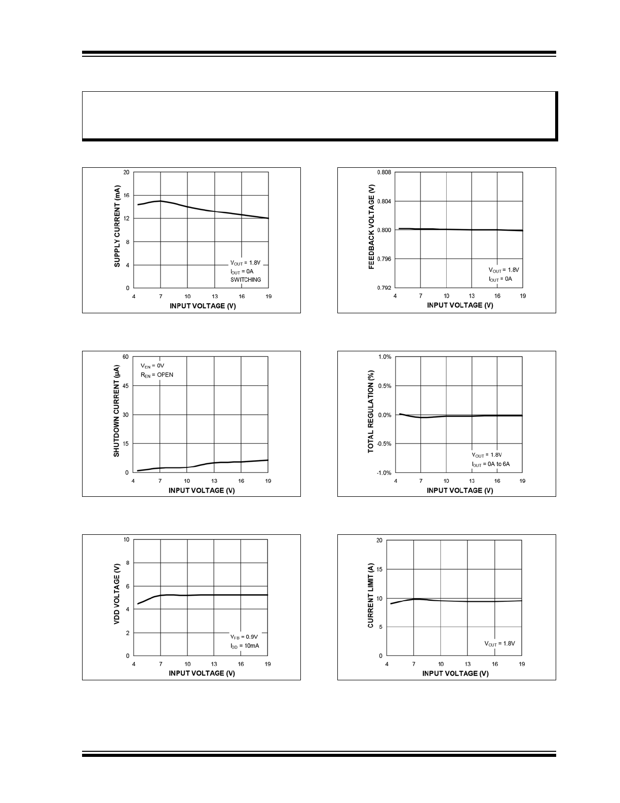
2.0
TYPICAL PERFORMANCE CURVES
FIGURE 2-1:
V
IN
Operating Supply
Current vs. Input Voltage.
FIGURE 2-2:
V
IN
Shutdown Current vs.
Input Voltage.
FIGURE 2-3:
V
DD
Output Voltage vs.
Input Voltage.
FIGURE 2-4:
Feedback Voltage vs. Input
Voltage.
FIGURE 2-5:
Total Regulation vs. Input
Voltage.
FIGURE 2-6:
Output Current Limit vs.
Input Voltage.
Note:
The graphs and tables provided following this note are a statistical summary based on a limited number of
samples and are provided for informational purposes only. The performance characteristics listed herein
are not tested or guaranteed. In some graphs or tables, the data presented may be outside the specified
operating range (e.g., outside specified power supply range) and therefore outside the warranted range.
MIC24051
DS20005658A-page 8
2016 Microchip Technology Inc.
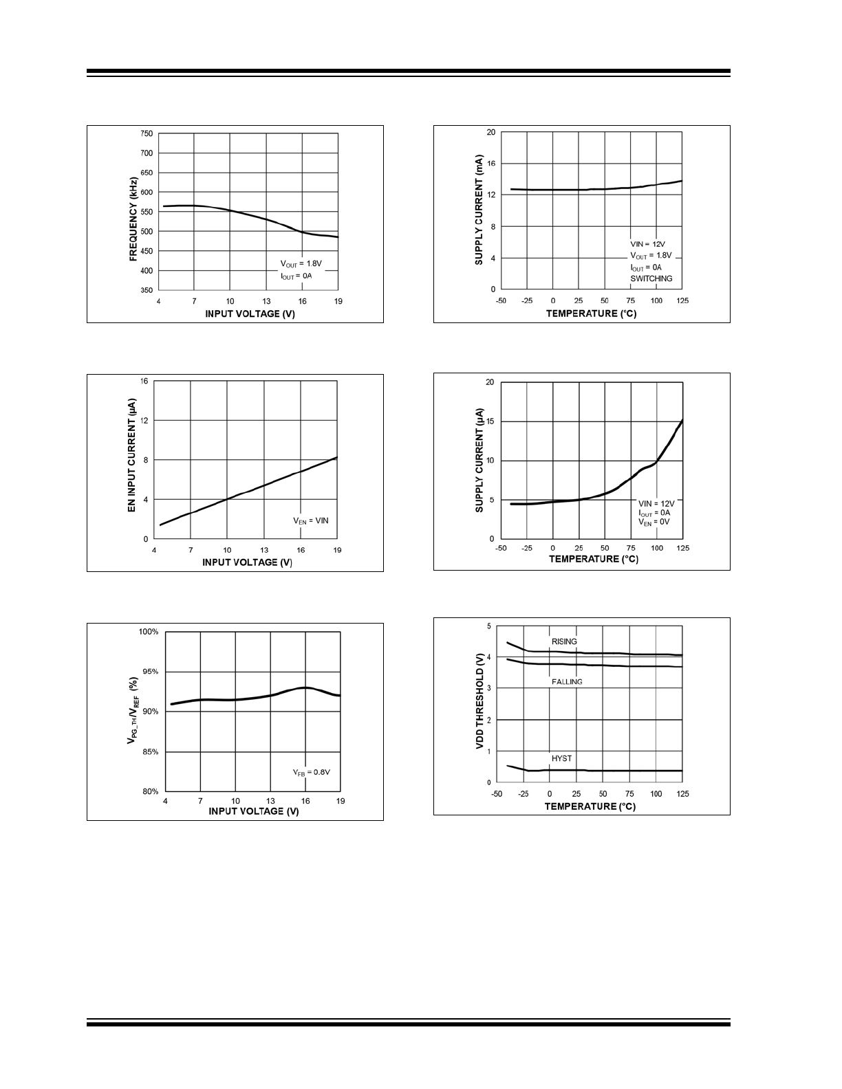
FIGURE 2-7:
Switching Frequency vs.
Input Voltage.
FIGURE 2-8:
Enable Input Current vs.
Input Voltage.
FIGURE 2-9:
PG Threshold/V
REF
Ratio
vs. Input Voltage.
FIGURE 2-10:
V
IN
Operating Supply
Current vs. Temperature.
FIGURE 2-11:
V
IN
Shutdown Current vs.
Temperature.
FIGURE 2-12:
V
DD
UVLO Threshold vs.
Temperature.
2016 Microchip Technology Inc.
DS20005658A-page 9
MIC24051
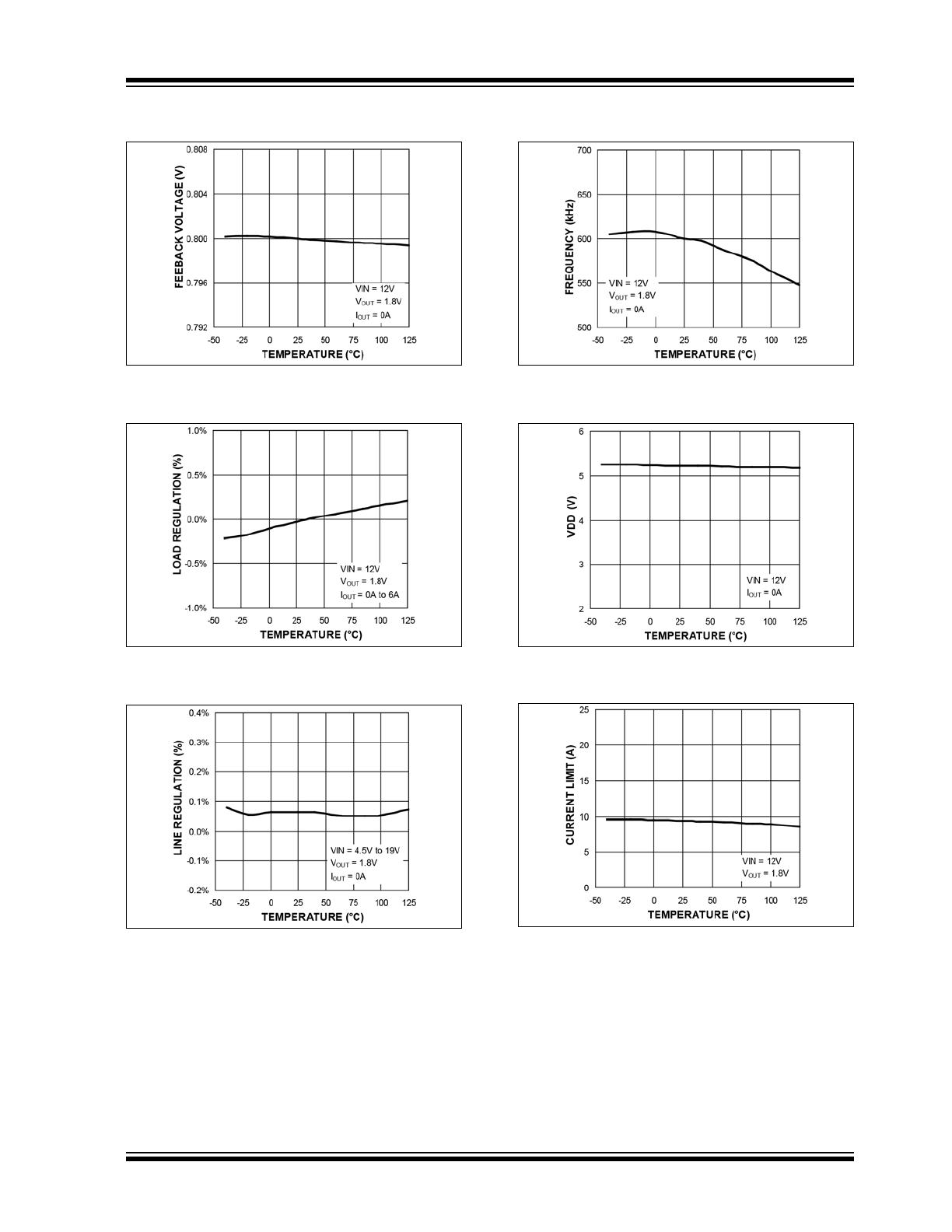
FIGURE 2-13:
Feedback Voltage vs.
Temperature
.
FIGURE 2-14:
Load Regulation vs.
Temperature
.
FIGURE 2-15:
Line Regulation vs.
Temperature.
FIGURE 2-16:
Switching Frequency vs.
Temperature
.
FIGURE 2-17:
V
DD
vs. Temperature
.
FIGURE 2-18:
Output Current Limit vs.
Temperature
.
MIC24051
DS20005658A-page 10
2016 Microchip Technology Inc.
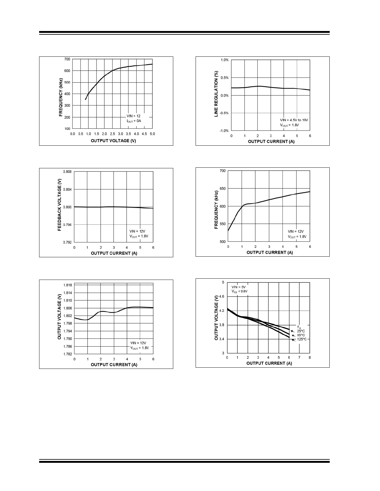
FIGURE 2-19:
Switching Frequency vs.
Output Voltage.
FIGURE 2-20:
Feedback Voltage vs.
Output Current.
FIGURE 2-21:
Output Voltage vs. Output
Current.
FIGURE 2-22:
Line Regulation vs. Output
Current.
FIGURE 2-23:
Switching Frequency vs.
Output Current.
FIGURE 2-24:
Output Voltage (V
IN
= 5V)
vs. Output Current.