
© 2009 Microchip Technology Inc.
DS22039D-page 1
MCP4725
Features
• 12-Bit Resolution
• On-Board Non-Volatile Memory (EEPROM)
• ±0.2 LSB DNL (typical)
• External A0 Address Pin
• Normal or Power-Down Mode
• Fast Settling Time: 6 µs (typical)
• External Voltage Reference (V
DD
)
• Rail-to-Rail Output
• Low Power Consumption
• Single-Supply Operation: 2.7V to 5.5V
• I
2
C
TM
Interface:
- Eight Available Addresses
- Standard (100 kbps), Fast (400 kbps), and
High-Speed (3.4 Mbps) Modes
• Small 6-lead SOT-23 Package
• Extended Temperature Range: -40°C to +125°C
Applications
• Set Point or Offset Trimming
• Sensor Calibration
• Closed-Loop Servo Control
• Low Power Portable Instrumentation
• PC Peripherals
• Data Acquisition Systems
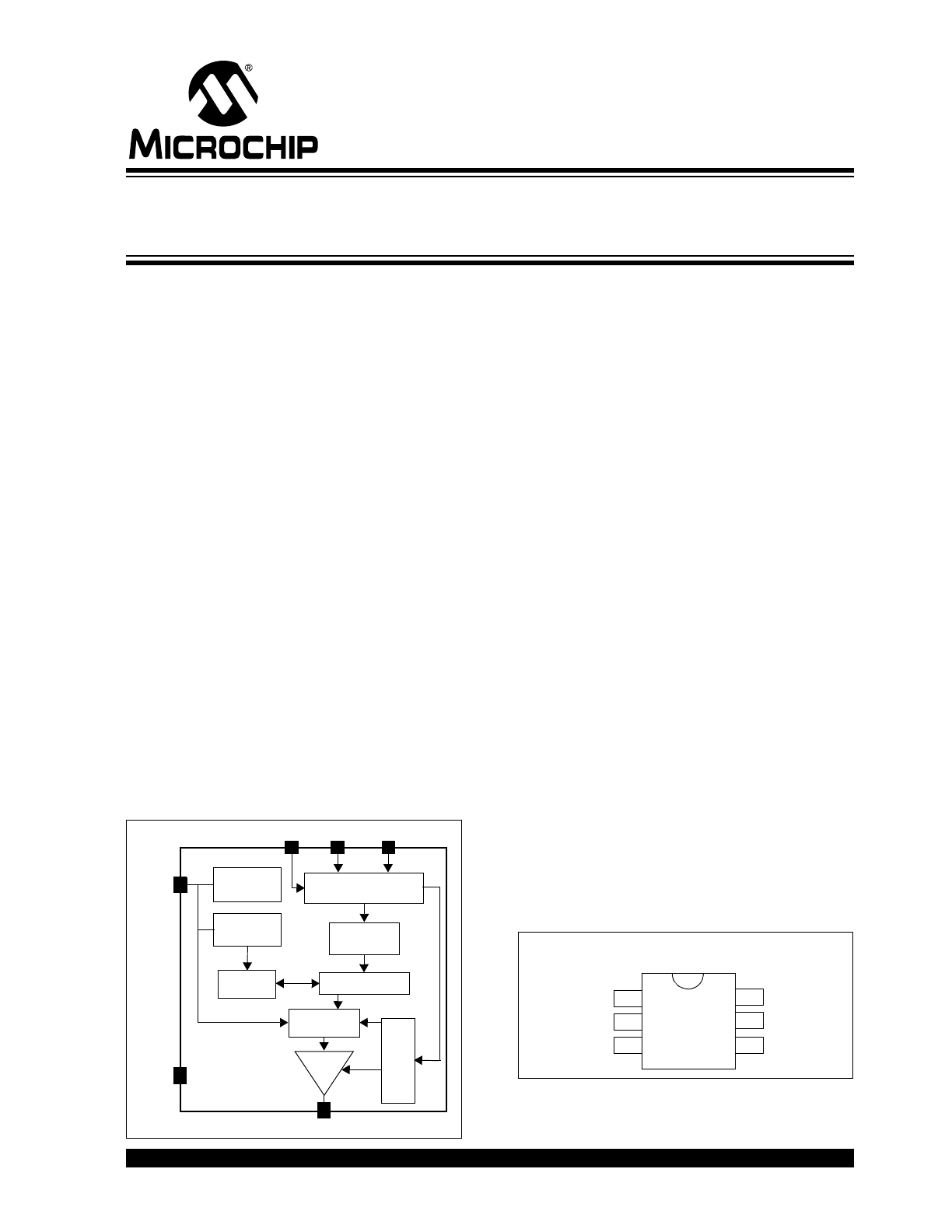
Block Diagram
DESCRIPTION
The MCP4725 is a low-power, high accuracy, single
channel, 12-bit buffered voltage output Digital-to-
Analog Convertor (DAC) with non-volatile memory
(EEPROM). Its on-board precision output amplifier
allows it to achieve rail-to-rail analog output swing.
The DAC input and configuration data can be
programmed to the non-volatile memory (EEPROM) by
the user using I
2
C interface command. The non-volatile
memory feature enables the DAC device to hold the
DAC input code during power-off time, and the DAC
output is available immediately after power-up. This
feature is very useful when the DAC device is used as
a supporting device for other devices in the network.
The device includes a Power-On-Reset (POR) circuit to
ensure reliable power-up and an on-board charge
pump for the EEPROM programming voltage. The
DAC reference is driven from V
DD
directly. In power-
down mode, the output amplifier can be configured to
present a known low, medium, or high resistance
output load.
The MCP4725 has an external A0 address bit selection
pin. This A0 pin can be tied to V
DD
or V
SS
of the user’s
application board.
The MCP4725 has a two-wire I
2
C™ compatible serial
interface for standard (100 kHz), fast (400 kHz), or high
speed (3.4 MHz) mode.
The MCP4725 is an ideal DAC device where design
simplicity and small footprint is desired, and for
applications requiring the DAC device settings to be
saved during power-off time.
The device is available in a small 6-pin SOT-23
package.
Package Type
Resistive
Power-on
Reset
Charge
Pump
EEPROM
I
2
C Interface Logic
Input
Register
DAC Register
Op
Amp
P
o
wer-down Control
V
DD
V
SS
SCL
SDA
V
OUT
A0
String DAC
3
V
DD
SCL
SDA
V
SS
A0
SOT-23-6
V
OUT
2
1
4
5
6
MCP4725
12-Bit Digital-to-Analog Converter with EEPROM Memory
in SOT-23-6

MCP4725
DS22039D-page 2
© 2009 Microchip Technology Inc.
NOTES:
© 2009 Microchip Technology Inc.
DS22039D-page 3
MCP4725
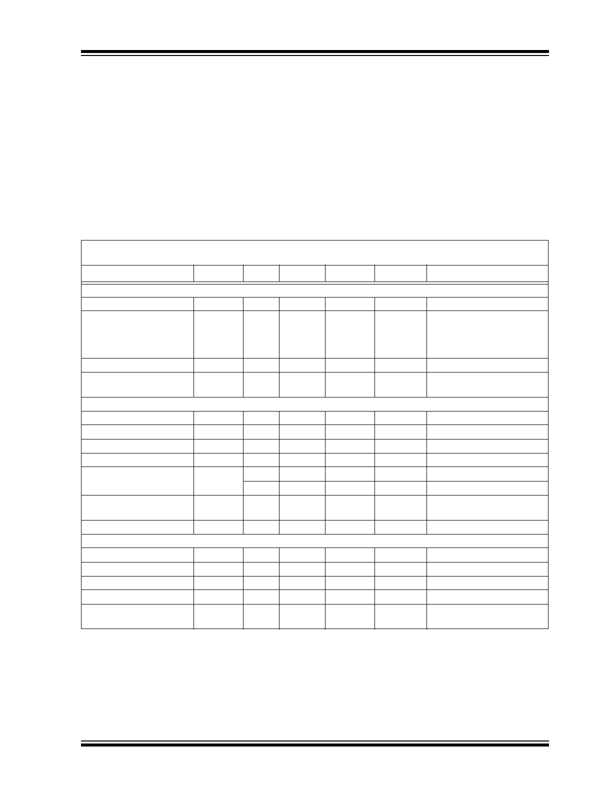
1.0
ELECTRICAL
CHARACTERISTICS
Absolute Maximum Ratings†
V
DD
...................................................................................6.5V
All inputs and outputs w.r.t V
SS
.................–0.3V to V
DD
+0.3V
Current at Input Pins ....................................................±2 mA
Current at Supply Pins ...............................................±50 mA
Current at Output Pins ...............................................±25 mA
Storage Temperature ...................................-65°C to +150°C
Ambient Temp. with Power Applied .............-55°C to +125°C
ESD protection on all pins
................ ≥ 6 kV HBM, ≥ 400V MM
Maximum Junction Temperature (T
J
) ......................... +150°C
† Notice: Stresses above those listed under “Maximum
ratings” may cause permanent damage to the device. This is
a stress rating only and functional operation of the device at
these or any other conditions above those indicated in the
operation listings of this specification is not implied. Exposure
to maximum rating conditions for extended periods may affect
device reliability
ELECTRICAL CHARACTERISTICS
Electrical Specifications: Unless otherwise indicated, all parameters apply at
V
DD
= + 2.7V to 5.5V,
V
SS
= 0V,
R
L
= 5 kΩ from V
OUT
to V
SS
, C
L
= 100 pF, T
A
= -40°C to +125°C. Typical values are at +25°C.
Parameter Sym
Min
Typ
Max Units
Conditions
Power Requirements
Operating Voltage
V
DD
2.7
5.5 V
Supply Current
I
DD
—
210
400
µA
Digital input pins are
grounded, Output pin (V
OUT
)
is not connected (unloaded),
Code = 000h
Power-Down Current
I
DDP
—
0.06
2.0
µA
V
DD
= 5.5V
Power-On-Reset
Threshold Voltage
V
POR
—
2
—
V
DC Accuracy
Resolution
n
12
—
—
Bits
Code Range = 000h to FFFh
INL Error
INL
—
±2
±14.5
LSB
Note 1
DNL DNL
-0.75
±0.2
±0.75
LSB
Note 1
Offset Error
V
OS
0.02
0.75
% of FSR Code = 000h
Offset Error Drift
ΔV
OS
/°C —
±1
—
ppm/°C
-45°C
to
+25°C
—
±2 —
ppm/°C
+25°C
to
+85°C
Gain Error
G
E
-2
-0.1
2
% of FSR Code = FFFh,
Offset error is not included.
Gain Error Drift
ΔG
E
/°C —
-3
—
ppm/°C
Output Amplifier
Phase Margin
p
M
—
66 —
Degree(°) C
L
= 400 pF, R
L
=
∞
Capacitive Load Stability
C
L
—
—
1000 pF
R
L
= 5 kΩ, Note 2
Slew Rate
SR
—
0.55
—
V/µs
Short Circuit Current
I
SC
—
15
24
mA
V
DD
= 5V, V
OUT
= Grounded
Output Voltage Settling
Time
T
S
—
6
—
µs
Note 3
Note 1: Test Code Range: 100 to 4000.
2: This parameter is ensure by design and not 100% tested.
3: Within 1/2 LSB of the final value when code changes from 1/4 to 3/4 (400h to C00h) of full scale range.
4: Logic state of external address selection pin (A0 pin).
MCP4725
DS22039D-page 4
© 2009 Microchip Technology Inc.
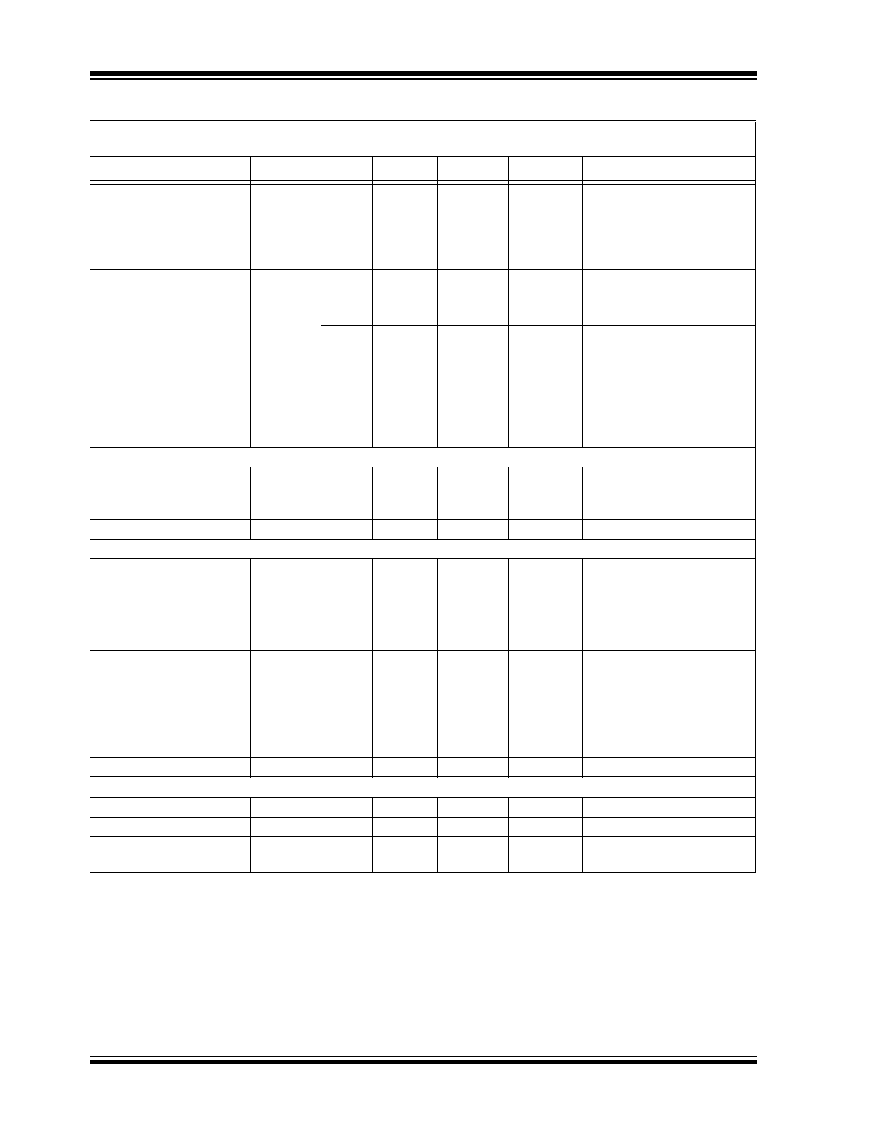
Power Up Time
T
PU
—
2.5
—
µs
V
DD
= 5V
—
5
—
µs
V
DD
= 3V
Exit Power-down Mode,
(Started from falling edge of
ACK pulse)
DC Output Impedance
R
OUT
—
1
—
Ω
Normal mode (V
OUT
to V
SS
)
—
1
—
k
Ω
Power-Down Mode 1
(V
OUT
to V
SS
)
—
100
—
k
Ω
Power-Down Mode 2
(V
OUT
to V
SS
)
—
500
—
k
Ω
Power-Down Mode 3
(V
OUT
to V
SS
)
Supply Voltage Power-up
Ramp Rate for EEPROM
loading
V
DD_RAMP
1
—
—
V/ms
Validation only.
Dynamic Performance
Major Code Transition
Glitch
—
45
—
nV-s
1 LSB change around major
carry (from 800h to 7FFh)
(Note 2)
Digital Feedthrough
—
<10
—
nV-s
Note 2
Digital Interface
Output Low Voltage
V
OL
—
—
0.4
V I
OL
= 3 mA
Input High Voltage
(SDA and SCL Pins)
V
IH
0.7V
DD
—
—
V
Input Low Voltage
(SDA and SCL Pins)
V
IL
—
—
0.3V
DD
V
Input High Voltage
(A0 Pin)
V
A0-Hi
0.8V
DD
—
—
Note 4
Input Low Voltage
(A0 Pin)
V
A0-IL
—
—
0.2V
DD
Note 4
Input Leakage
I
LI
—
—
±1
µA
SCL = SDA = A0 = V
SS
or
SCL = SDA = A0 = V
DD
Pin Capacitance
C
PIN
—
—
3
pF
Note 2
EEPROM
EEPROM Write Time
T
WRITE
—
25
50
ms
Data Retention
—
200
—
Years
At +25°C, (Note 2)
Endurance
1
—
—
Million
Cycles
At +25°C, (Note 2)
ELECTRICAL CHARACTERISTICS (CONTINUED)
Electrical Specifications: Unless otherwise indicated, all parameters apply at
V
DD
= + 2.7V to 5.5V,
V
SS
= 0V,
R
L
= 5 kΩ from V
OUT
to V
SS
, C
L
= 100 pF, T
A
= -40°C to +125°C. Typical values are at +25°C.
Parameter Sym
Min
Typ
Max Units
Conditions
Note 1: Test Code Range: 100 to 4000.
2: This parameter is ensure by design and not 100% tested.
3: Within 1/2 LSB of the final value when code changes from 1/4 to 3/4 (400h to C00h) of full scale range.
4: Logic state of external address selection pin (A0 pin).
© 2009 Microchip Technology Inc.
DS22039D-page 5
MCP4725
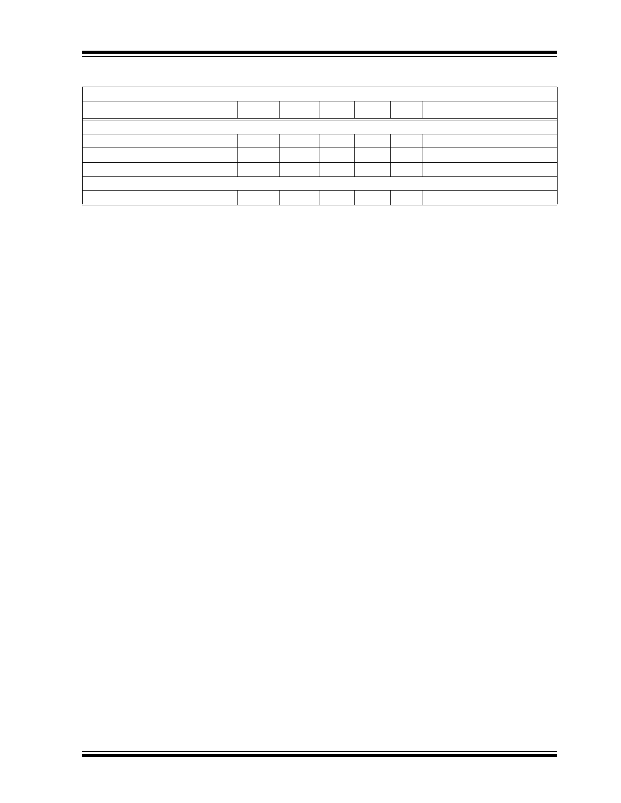
TEMPERATURE CHARACTERISTICS
Electrical Specifications: Unless otherwise indicated, V
DD
= +2.7V to +5.5V, V
SS
= GND.
Parameters
Sym
Min
Typ
Max
Units
Conditions
Temperature Ranges
Specified Temperature Range
T
A
-40
—
+125
°C
Operating Temperature Range
T
A
-40
—
+125
°C
Storage Temperature Range
T
A
-65
—
+150
°C
Thermal Package Resistances
Thermal Resistance, 6L-SOT-23
θ
JA
—
190.5
—
°C/W

MCP4725
DS22039D-page 6
© 2009 Microchip Technology Inc.
NOTES:
© 2009 Microchip Technology Inc.
DS22039D-page 7
MCP4725
2.0
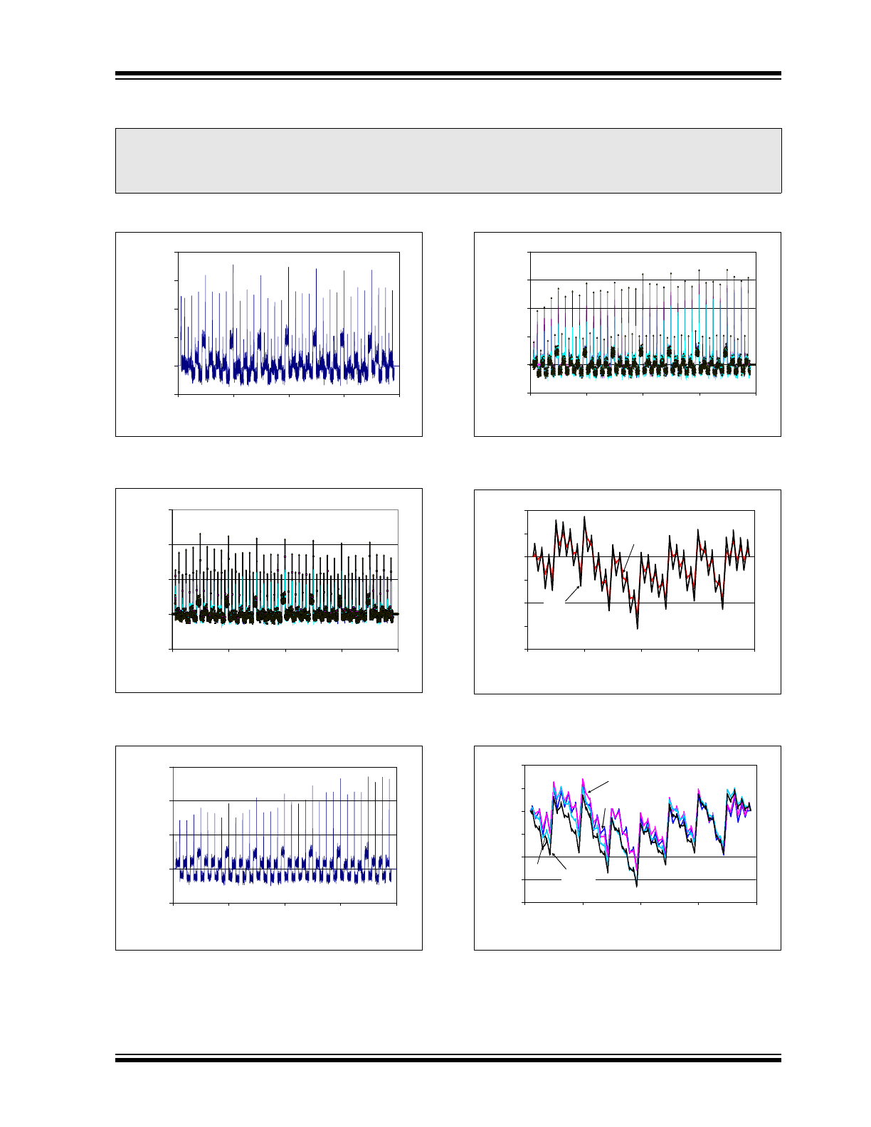
TYPICAL PERFORMANCE CURVES
Note: Unless otherwise indicated, T
A
= +25°C, V
DD
= +5.0V, V
SS
= 0V, R
L
= 5 kΩ to V
SS
, C
L
= 100 pF.
FIGURE 2-1:
DNL vs. Code (V
DD
= 5.5V).
FIGURE 2-2:
DNL vs. Code and
Temperature (T
A
= -40°C to +125°C).
FIGURE 2-3:
DNL vs. Code (V
DD
= 2.7V).
FIGURE 2-4:
DNL vs. Code and
Temperature (T
A
= -40°C to +125°C).
FIGURE 2-5:
INL vs. Code.
FIGURE 2-6:
INL vs. Code and
Temperature (V
DD
= 5.5V).
Note:
The graphs and tables provided following this note are a statistical summary based on a limited number of
samples and are provided for informational purposes only. The performance characteristics listed herein
are not tested or guaranteed. In some graphs or tables, the data presented may be outside the specified
operating range (e.g., outside specified power supply range) and therefore, outside the warranted range.
-0.04
0
0.04
0.08
0.12
0.16
0
1024
2048
3072
4096
Code
DNL (
L
SB)
-0.1
0
0.1
0.2
0.3
0
1024
2048
3072
4096
Code
DNL (
L
SB)
V
DD
= 5.5V
-0.1
0.0
0.1
0.2
0.3
0
1024
2048
3072
4096
Code
DN
L
(
L
SB
)
-0.1
0.0
0.1
0.2
0.3
0.4
0
1024
2048
3072
4096
Code
DN
L
(L
SB
)
V
DD
= 2.7V
-4
-3
-2
-1
0
1
2
0
1024
2048
3072
4096
Code
IN
L(
LSB)
2.7V
5.5V
-4
-3
-2
-1
0
1
2
0
1024
2048
3072
4096
Code
IN
L(
L
S
B
)
+25°C
+125°C
- 40°C
+85°C
MCP4725
DS22039D-page 8
© 2009 Microchip Technology Inc.
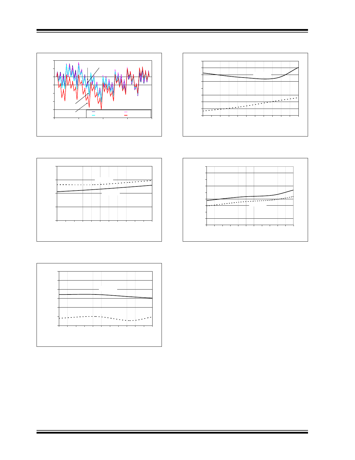
Note: Unless otherwise indicated, T
A
= +25°C, V
DD
= +5.0V, V
SS
= 0V, R
L
= 5 kΩ to V
SS
, C
L
= 100 pF.
FIGURE 2-7:
INL vs. Code and
Temperature (V
DD
= 2.7V).
FIGURE 2-8:
Zero Scale Error vs.
Temperature (Code = 000d).
FIGURE 2-9:
Full Scale Error vs.
Temperature (Code = 4095d).
FIGURE 2-10:
Output Error vs.
Temperature (Code = 4000d).
FIGURE 2-11:
I
DD
vs. Temperature.
-5
-4
-3
-2
-1
0
1
2
0
1024
2048
3072
4096
Code
IN
L
(L
S
B
)
TA = -40 C
TA = 25 C
TA = 85 C
TA = 125 C
+125°C
- 40°C
+85°C
+25°C
-1
0
1
2
3
-40 -25 -10 5
20 35 50 65 80 95 110 125
Temperature (°C)
Zero S
cale
Error (mV)
V
DD
= 5.5V
V
DD
= 2.7V
-60
-50
-40
-30
-20
-10
0
-40 -25 -10 5
20 35 50 65 80 95 110 125
Temperature (°C)
Full-
S
c
al
e E
rror (
m
V
)
V
DD
= 2.7V
V
DD
= 5.5V
-5
-4
-3
-2
-1
0
1
2
3
-40 -25 -10 5
20 35 50 65 80 95 110 125
Temperature (°C)
Out
p
ut
E
rror (
m
V
)
V
DD
= 2.7V
V
DD
= 5.5V
0
50
100
150
200
250
300
350
400
450
-40 -25 -10 5 20 35 50 65 80 95 110 125
Temperature(°C)
I
DD
(A)
V
DD
= 2.7V
V
DD
= 5V
© 2009 Microchip Technology Inc.
DS22039D-page 9
MCP4725
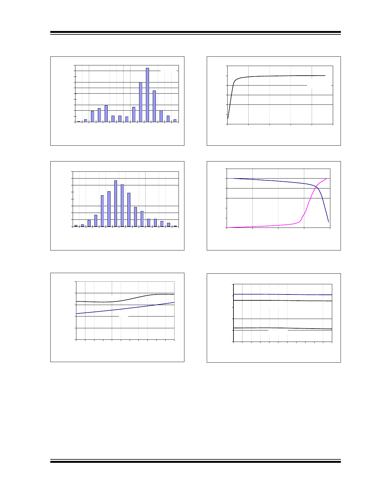
Note: Unless otherwise indicated, T
A
= +25°C, V
DD
= +5.0V, V
SS
= 0V, R
L
= 5 kΩ to V
SS
, C
L
= 100 pF.
FIGURE 2-12:
I
DD
Histogram .
FIGURE 2-13:
I
DD
Histogram.
FIGURE 2-14:
Offset Error vs. Temperature
and V
DD
.
FIGURE 2-15:
V
OUT
vs. Resistive Load.
FIGURE 2-16:
Source and Sink Current
Capability.
FIGURE 2-17:
V
IN
High Threshold vs.
Temperature and V
DD
.
0
10
20
30
40
50
60
70
80
90
100
18
0
18
4
18
8
19
2
19
6
20
0
20
4
20
8
21
2
21
6
22
0
22
4
22
8
23
2
23
6
Current (µA)
Oc
cura
nc
e
V
DD
= 5V
V
DD
= 2.7V
0
10
20
30
40
50
60
70
80
16
3
16
5
16
7
16
9
17
1
17
3
17
5
17
7
17
9
18
1
18
3
18
5
18
7
18
9
19
1
19
3
Current (µA)
Occ
u
ranc
e
0.00
0.50
1.00
1.50
2.00
2.50
-40 -25 -10 5
20 35 50 65 80 95 110 125
Temperature (°C)
Of
fse
t E
rror (
m
V
)
2.7V
5.5V
0
1
2
3
4
5
6
0
1
2
3
4
5
Load Resistance (kΩ)
V
OU
T
(V
)
V
DD
= 5V
Code = FFFh
0
1
2
3
4
5
6
0
4
8
12
16
I
SOURCE/SINK
(mA)
V
OUT
(V
)
Code = FFFh
Code = 000h
V
DD
= 5V
1.00
1.50
2.00
2.50
3.00
3.50
-40 -25 -10 5
20 35 50 65 80 95 110 125
Temperature (°C)
V
IH
Threshold (
V
)
V
DD
= 5.5V
V
DD
= 5.0V
V
DD
= 2.7V
MCP4725
DS22039D-page 10
© 2009 Microchip Technology Inc.
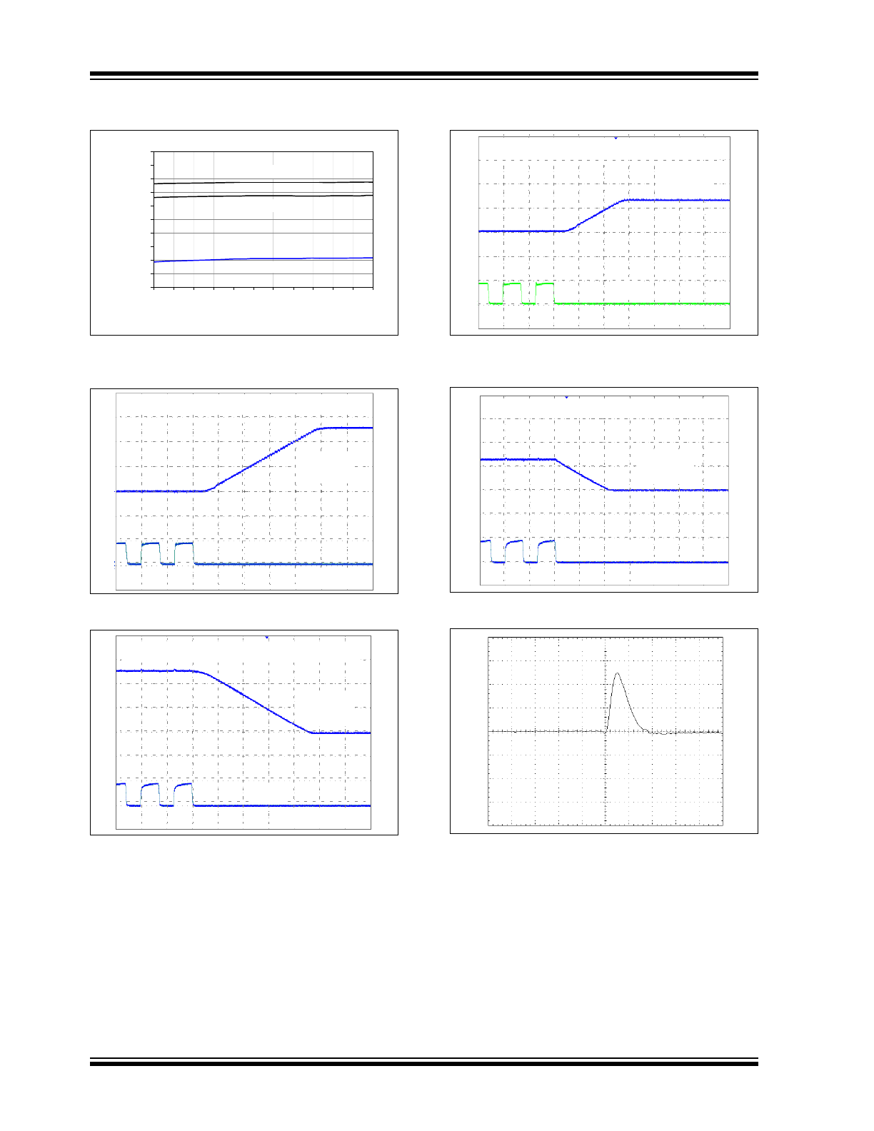
Note: Unless otherwise indicated, T
A
= +25°C, V
DD
= +5.0V, V
SS
= 0V, R
L
= 5 kΩ to V
SS
, C
L
= 100 pF.
FIGURE 2-18:
V
IN
Low Threshold vs.
Temperature and V
DD
.
FIGURE 2-19:
Full Scale Settling Time.
FIGURE 2-20:
Full Scale Settling Time.
FIGURE 2-21:
Half Scale Settling Time.
FIGURE 2-22:
Half Scale Settling Time.
FIGURE 2-23:
Code Change Glitch.
0.50
0.70
0.90
1.10
1.30
1.50
1.70
1.90
2.10
2.30
2.50
-40 -25 -10 5
20 35 50 65 80 95 110 125
Temperature (°C)
V
IL
T
h
re
s
hol
d (
V
)
V
DD
= 5.5V
V
DD
= 5.0V
V
DD
= 2.7V
Full Scale Code Change: 000h to FFFh
V
OUT
(2V/Div)
CLK
Time (2 µs/Div)
Full Scale Code Change: FFFh to 000h
V
OUT
(2V/Div)
CLK
Time (2 µs/Div)
Half Scale Code Change: 000h to 7FFh
V
OUT
(2V/Div)
CLK
Time (2 µs/Div)
V
OUT
(2V/Div)
CLK
Time (2 µs/Div)
Half Scale Code Change: 7FFh to 000h
Code Change: 800h to 7FFh
V
OUT
(20 mV/Div)
Time (1 µs/Div)