
2008-2018 Microchip Technology Inc.
DS20002122E-page 1
11AA02E48/11AA02E64
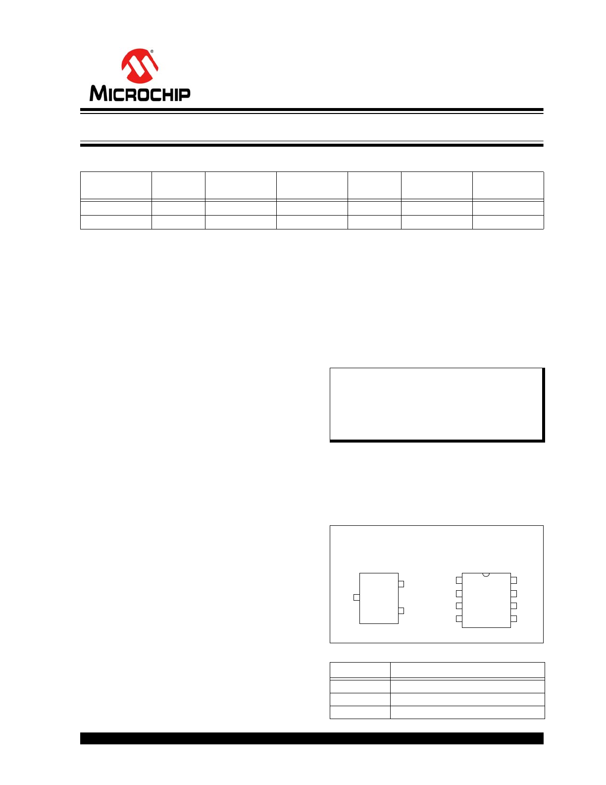
Device Selection Table
Features
• Preprogrammed Globally Unique, 48-Bit or 64-Bit
Node Address
• Compatible with EUI-48
™
and EUI-64
™
• Single I/O, UNI/O
®
Serial Interface Bus
• Low-Power CMOS Technology:
- 1 mA active current, typical
- 1 µA standby current, maximum
• 256 x 8-Bit Organization
• Schmitt Trigger Inputs for Noise Suppression
• Output Slope Control to Eliminate Ground Bounce
• 100 kbps Maximum Bit Rate – Equivalent to
100 kHz Clock Frequency
• Self-Timed Write Cycle (including Auto-Erase)
• Page-Write Buffer for up to 16 Bytes
• STATUS Register for Added Control:
- Write Enable Latch bit
- Write-In-Progress bit
• Block Write Protection:
- Protect none, 1/4, 1/2 or all of array
• Built-in Write Protection:
- Power-on/off data protection circuitry
- Write enable latch
• High Reliability:
- Endurance: 1,000,000 erase/write cycles
- Data retention: >200 years
- ESD protection: >4,000V
• 3-Lead SOT-23 and 8-Lead SOIC Packages
• Pb-Free and RoHS Compliant
• Available Temperature Ranges:
Description
The Microchip Technology Inc.
11AA02E48/11AA02E64 (11AA02EXX
(
1
)
) device is a
2 Kbit Serial Electrically Erasable PROM. The device is
organized in blocks of x8-bit memory and support the
patented
(
2
)
single I/O UNI/O
®
serial bus. By using
Manchester encoding techniques, the clock and data
are combined into a single, serial bit stream (SCIO),
where the clock signal is extracted by the receiver to
correctly decode the timing and value of each bit.
Low-voltage design permits operation down to 1.8V,
with standby and active currents of only 1 µA and
1 mA, respectively.
The 11AA02EXX is available in standard 8-lead
SOIC and 3-lead SOT-23 packages.
Package Types (not to scale)
Pin Function Table
Part Number
Density
(bits)
V
CC
Range
Page Size
(Bytes)
Temp.
Ranges
Packages
Node Address
11AA02E48
2K
1.8V-5.5V
16
I
SN, TT
EUI-48
™
11AA02E64
2K
1.8V-5.5V
16
I
SN, TT
EUI-64
™
- Industrial (I):
-40°C to
+85°C
Note 1:
11AA02EXX is used in this document as
a generic part number for the 11AA02E48
and 11AA02E64 devices.
2:
Microchip’s UNI/O
®
Bus products are
covered by the following patents issued
in the U.S.A.: 7,376,020 and 7,788,430.
Name
Function
SCIO
Serial Clock, Data Input/Output
V
SS
Ground
V
CC
Supply Voltage
V
CC
SCIO
V
SS
3-Lead SOT-23
(TT)
NC
NC
NC
V
SS
V
CC
NC
NC
SCIO
1
2
3
4
8
7
6
5
SOIC
(SN)
3
2
1
2K UNI/O
®
Serial EEPROMs with EUI-48
™
or EUI-64
™
Node Identity

2008-2018 Microchip Technology Inc.
DS20002122E-page 2
11AA02E48/11AA02E64
1.0
ELECTRICAL CHARACTERISTICS
Absolute Maximum Ratings
(†)
V
CC
.............................................................................................................................................................................6.5V
SCIO w.r.t. V
SS
.....................................................................................................................................-0.6V to V
CC
+1.0V
Storage temperature ................................................................................................................................. -65°C to 150°C
Ambient temperature under bias................................................................................................................. -40°C to 85°C
ESD protection on all pins.......................................................................................................................................... 4 kV
TABLE 1-1:
DC CHARACTERISTICS
† NOTICE:
Stresses above those listed under ‘Absolute Maximum Ratings’ may cause permanent damage to the
device. This is a stress rating only and functional operation of the device at those or any other conditions above those
indicated in the operational listings of this specification is not implied. Exposure to maximum rating conditions for an
extended period of time may affect device reliability.
DC CHARACTERISTICS
Electrical Characteristics:
Industrial (I):
V
CC
= 2.5V to 5.5V
T
A
= -40°C to +85°C
V
CC
= 1.8V to 2.5V
T
A
= -20°C to +85°C
Param.
No.
Symbol
Characteristic
Min.
Max.
Units
Test Conditions
D1
V
IH
High-Level Input
Voltage
0.7 V
CC
V
CC
+1
V
D2
V
IL
Low-Level Input
Voltage
-0.3
0.3 V
CC
V
V
CC
≥ 2.5V
-0.3
0.2 V
CC
V
V
CC
< 2.5V
D3
V
HYS
Hysteresis of Schmitt
Trigger Inputs
(SCIO)
0.05 Vcc
—
V
V
CC
≥ 2.5V (
Note 1
)
D4
V
OH
High-Level Output
Voltage
V
CC
-0.5
—
V
I
OH
= -300 µA, V
CC
= 5.5V
V
CC
-0.5
—
V
I
OH
= -200 µA, Vcc = 2.5V
D5
V
OL
Low-Level Output
Voltage
—
0.4
V
I
O
I = 300 µA, V
CC
= 5.5V
—
0.4
V
I
O
I = 200 µA, Vcc = 2.5V
D6
I
O
Output Current Limit
(
Note 2
)
—
±4
mA
V
CC
= 5.5V (
Note 1
)
—
±3
mA
Vcc = 2.5V (
Note 1
)
D7
I
LI
Input Leakage
Current (SCIO)
—
±1
µA
V
IN
= V
SS
or V
CC
D8
C
INT
Internal Capacitance
(all inputs and
outputs)
—
7
pF
T
A
= 25°C, F
CLK
= 1 MHz,
V
CC
= 5.0V (
Note 1
)
D9
I
CCREAD
Read
Operating
Current
—
3
mA
V
CC
= 5.5V, F
BUS
= 100 kHz,
C
B
= 100 pF
—
1
mA
V
CC
= 2.5V, F
BUS
= 100 kHz,
C
B
= 100 pF
D10
I
CCWRITE
Write Operating
Current
—
5
mA
V
CC
= 5.5V
—
3
mA
V
CC
= 2.5V
D11
Iccs
Standby Current
—
1
µA
V
CC
= 5.5V, T
A
= 85°C
D12
I
CCI
Idle Mode Current
—
50
µA
V
CC
= 5.5V
Note 1:
This parameter is periodically sampled and not 100% tested.
2:
The SCIO output driver impedance will vary to ensure I
O
is not exceeded.

2008-2018 Microchip Technology Inc.
DS20002122E-page 3
11AA02E48/11AA02E64
TABLE 1-3:
AC TEST CONDITIONS
TABLE 1-2:
AC CHARACTERISTICS
AC CHARACTERISTICS
Electrical Characteristics:
Industrial (I):
V
CC
= 2.5V to 5.5V
T
A
= -40°C to +85°C
V
CC
= 1.8V to 2.5V
T
A
= -20°C to +85°C
Param.
No.
Symbol
Characteristic
Min.
Max.
Units
Test Conditions
1
F
BUS
Serial Bus
Frequency
10
100
kHz
2
T
E
Bit Period
10
100
µs
3
T
IJIT
Input Edge Jitter
Tolerance
—
±0.06
UI
Note 2
4
F
DRIFT
Serial Bus
Frequency Drift Rate
Tolerance
—
±0.50
% per byte
5
F
DEV
Serial Bus
Frequency Drift Limit
—
±5
% per command
6
T
OJIT
Output Edge Jitter
—
±0.25
UI
Note 2
7
T
R
SCIO Input Rise
Time (
Note 1
)
—
100
ns
8
T
F
SCIO Input Fall Time
(
Note 1
)
—
100
ns
9
T
STBY
Standby Pulse Time
600
—
µs
10
T
SS
Start Header Setup
Time
10
—
µs
11
T
HDR
Start Header Low
Pulse Time
5
—
µs
12
T
SP
Input Filter Spike
Suppression (SCIO)
—
50
ns
Note 1
13
T
WC
Write Cycle Time
(byte or page)
—
5
ms
Write, WRSR commands
10
ms
ERAL, SETAL commands
14
Endurance (per
page)
1M
—
cycles
25°C, V
CC
= 5.5V (
Note 3
)
Note 1:
This parameter is periodically sampled and not 100% tested.
2:
A Unit Interval (UI) is equal to 1-bit period (T
E
) at the current bus frequency.
3:
This parameter is not tested but ensured by characterization. For endurance estimates in a specific
application, please consult the Total Endurance
™
Model which can be obtained on Microchip’s website:
www.microchip.com.
AC Waveform
V
LO
= 0.2V
V
HI
= V
CC
- 0.2V
C
L
= 100 pF
Timing Measurement Reference Level
Input
0.5 V
CC
Output
0.5 V
CC
2008-2018 Microchip Technology Inc.
DS20002122E-page 4
11AA02E48/11AA02E64
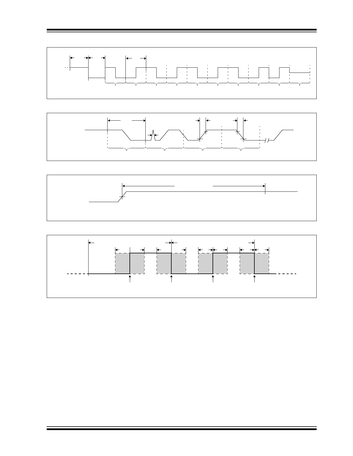
FIGURE 1-1:
BUS TIMING – START HEADER
FIGURE 1-2:
BUS TIMING – DATA
FIGURE 1-3:
BUS TIMING – STANDBY PULSE
FIGURE 1-4:
BUS TIMING – JITTER
SCIO
2
Data ‘0’ Data ‘1’ Data ‘0’ Data ‘1’ Data ‘0’ Data ‘1’ Data ‘0’ Data ‘1’ MAK bit NoSAK bit
11
10
2
SCIO
7
8
Data ‘0’
Data ‘1’
Data ‘1’
Data ‘0’
12
SCIO
9
Standby
Mode
Ideal Edge
3
2
3
6
6
2
6
6
Ideal Edge
Ideal Edge
Ideal Edge
from Master
from Master
from Slave
from Slave
2008-2018 Microchip Technology Inc.
DS20002122E-page 5
11AA02E48/11AA02E64
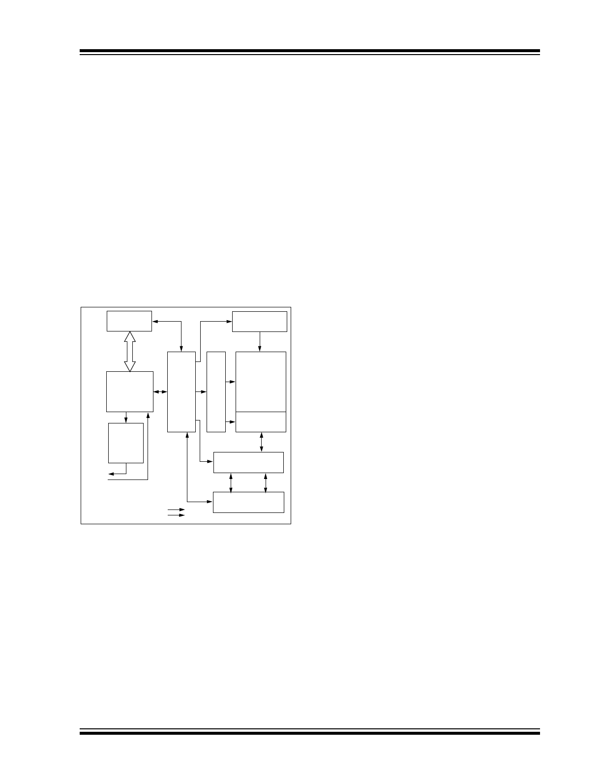
2.0
FUNCTIONAL DESCRIPTION
2.1
Principles of Operation
The 11AA02EXX family of serial EEPROMs support
the UNI/O
®
protocol. They can be interfaced with
microcontrollers, including Microchip’s PIC
®
microcontrollers, ASICs, or any other device with an
available discrete I/O line that can be configured
properly to match the UNI/O protocol.
The 11AA02EXX devices contain an 8-bit instruction
register. The devices are accessed via the SCIO pin.
Data is embedded into the I/O stream through
Manchester encoding. The bus is controlled by a
master device which determines the clock period,
controls the bus access and initiates all operations,
while the 11AA02EXX works as slave. Both master
and slave can operate as transmitter or receiver, but
the master device determines which mode is active.
FIGURE 2-1:
BLOCK DIAGRAM
SCIO
STATUS
Register
I/O Control
Memory
Control
Logic
X
Dec
HV Generator
EEPROM
Array
Page Latches
Y Decoder
Sense Amp.
R/W Control
Logic
V
CC
V
SS
Current-
Limited
Slope
Control
2008-2018 Microchip Technology Inc.
DS20002122E-page 6
11AA02E48/11AA02E64
3.0
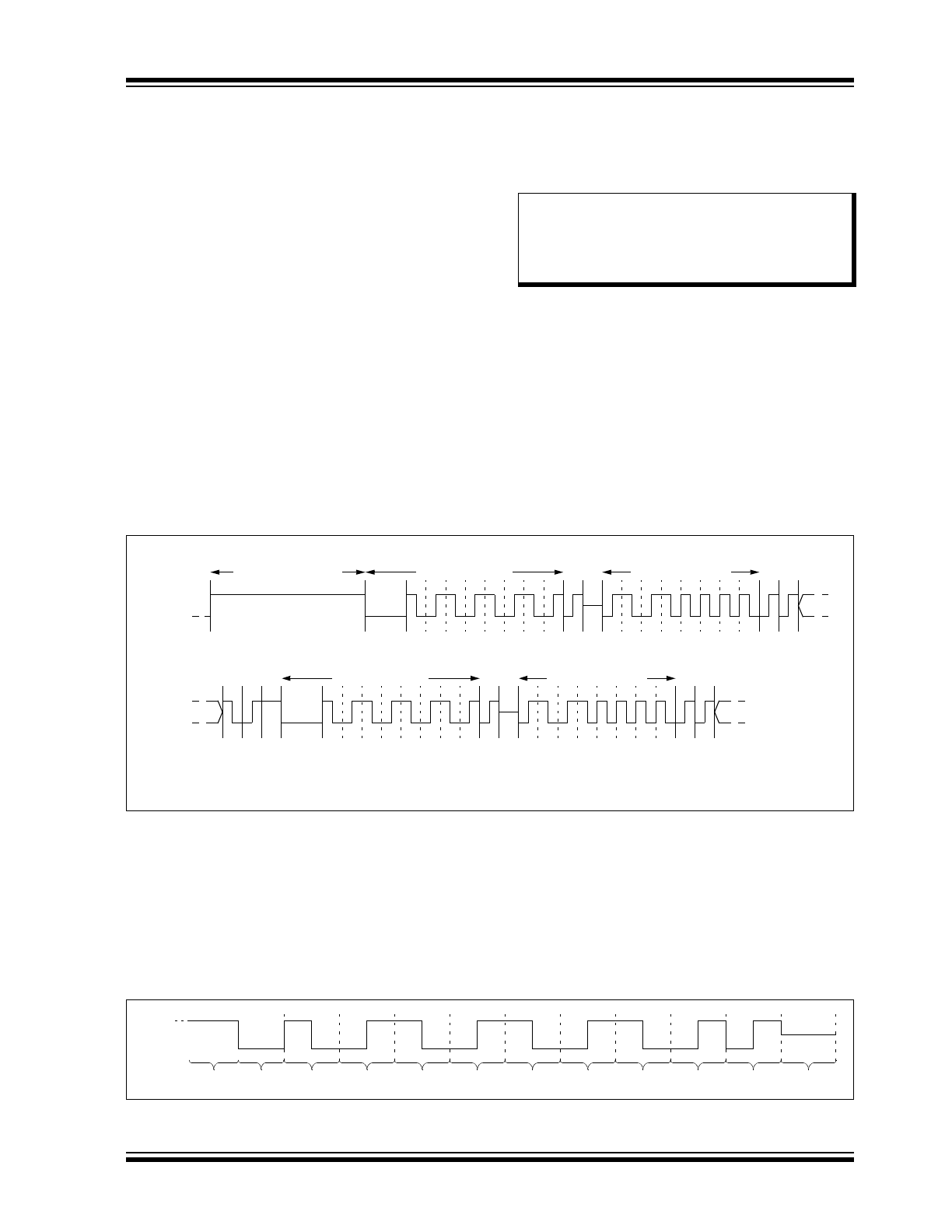
BUS CHARACTERISTICS
3.1
Standby Pulse
When the master has control of SCIO, a standby pulse
can be generated by holding SCIO high for T
STBY
. At
this time, the 11AA02EXX will reset and return to
Standby mode. Subsequently, a high-to-low transition
on SCIO (the first low pulse of the header) will return
the device to the active state.
Once a command is terminated satisfactorily (i.e., via
a NoMAK/SAK combination during the Acknowledge
sequence), performing a standby pulse is not required
to begin a new command as long as the device to be
selected is the same device selected during the
previous command. However, a period of T
SS
must be
observed after the end of the command and before the
beginning of the start header. After T
SS
, the start
header (including T
HDR
low pulse) can be transmitted
in order to begin the new command.
If a command is terminated in any manner other than a
NoMAK/SAK combination, then the master must
perform a standby pulse before beginning a new
command, regardless of which device is to be selected
.
An example of two consecutive commands is shown in
Figure 3-1
. Note that the device address is the same
for both commands, indicating that the same device is
being selected both times.
A standby pulse cannot be generated while the slave
has control of SCIO. In this situation, the master must
wait for the slave to finish transmitting and to release
SCIO before the pulse can be generated.
If, at any point during a command, an error is detected
by the master, a standby pulse should be generated
and the command should be performed again.
FIGURE 3-1:
CONSECUTIVE COMMANDS EXAMPLE
3.2
Start Data Transfer
All operations must be preceded by a start header. The
start header consists of holding SCIO low for a period
of T
HDR
, followed by transmitting an 8-bit ‘01010101’
code. This code is used to synchronize the slave’s
internal clock period with the master’s clock period, so
accurate timing is very important.
When a standby pulse is not required (i.e., between
successive commands to the same device), a period of
T
SS
must be observed after the end of the command
and before the beginning of the start header.
Figure 3-2
shows the waveform for the start header,
including the required Acknowledge sequence at the
end of the byte.
FIGURE 3-2:
START HEADER
Note:
After a POR/BOR event occurs, a
low-to-high transition on SCIO must be
generated before proceeding with
communication, including a standby
pulse.
1
1
0
1
0
1
0
0
Start Header
SCIO
Device Address
MA
K
0
0
0
0
1
0
1
0
MA
K
NoSAK
SAK
Standby Pulse
(1)
1
1
0
1
0
1
0
0
Start Header
SCIO
Device Address
MA
K
0
0
0
0
1
0
1
0
MA
K
NoSAK
SA
K
No
M
A
K
SA
K
T
SS
Note 1:
After a POR/BOR event, a low-to-high transition on SCIO is required to occur before the first
standby pulse.
SCIO
Data ‘0’ Data ‘1’ Data ‘0’ Data ‘1’ Data ‘0’ Data ‘1’ Data ‘0’ Data ‘1’
MAK
NoSAK
T
SS
T
HDR
2008-2018 Microchip Technology Inc.
DS20002122E-page 7
11AA02E48/11AA02E64
3.3
Acknowledge
An Acknowledge routine occurs after each byte is
transmitted, including the start header. This routine
consists of two bits. The first bit is transmitted by the
master, and the second bit is transmitted by the slave.
The Master Acknowledge, or MAK, is signified by
transmitting a ‘1’, and informs the slave that the current
operation is to be continued. Conversely, a Not
Acknowledge, or NoMAK, is signified by transmitting a
‘0’, and is used to end the current operation (and initiate
the write cycle for write operations).
The slave Acknowledge, or SAK, is also signified by
transmitting a ‘1’, and confirms proper communication.
However, unlike the NoMAK, the NoSAK is signified by
the lack of a middle edge during the bit period.
A NoSAK will occur for the following events:
• Following the start header
• Following the device address, if no slave on the
bus matches the transmitted address
• Following the command byte, if the command is
invalid, including Read, CRRD, Write, WRSR,
SETAL, and ERAL during a write cycle.
• If the slave becomes out of sync with the master
• If a command is terminated prematurely by using
a NoMAK, with the exception of immediately after
the device address.
See
Figure 3-3
and
Figure 3-4
for details.
If a NoSAK is received from the slave after any byte
(except the start header), an error has occurred. The
master should then perform a standby pulse and begin
the desired command again.
FIGURE 3-3:
ACKNOWLEDGE
ROUTINE
FIGURE 3-4:
ACKNOWLEDGE BITS
3.4
Device Addressing
A device address byte is the first byte received from the
master device following the start header. The device
address byte consists of a four-bit family code, for the
11AA02EXX this is set as ‘1010’. The last four bits of
the device address byte are the device code, which is
hardwired to ‘0000’.
FIGURE 3-5:
DEVICE ADDRESS BYTE
ALLOCATION
3.5
Bus Conflict Protection
To help guard against high-current conditions arising
from bus conflicts, the 11AA02EXX features a
current-limited output driver. The I
OL
and I
OH
specifications describe the maximum current that can
be sunk or sourced, respectively, by the SCIO pin. The
11AA02EXX will vary the output driver impedance to
ensure that the maximum current level is not exceeded.
Note:
A MAK must always be transmitted
following the start header.
Note:
When a NoMAK is used to end a WRITE or
WRSR
instruction, the write cycle is not
initiated if no bytes of data have been
received.
Note:
In order to guard against bus contention, a
NoSAK will occur after the start header.
Master
Slave
MAK
SAK
MAK (‘1’)
NoMAK (‘0’)
SAK (‘1’)
NoSAK
(1)
Note 1:
valid SAK.
A NoSAK is defined as any sequence that is not a
1
0
1
0
0
0
0
MAK
SLAVE ADDRESS
0
SAK

2008-2018 Microchip Technology Inc.
DS20002122E-page 8
11AA02E48/11AA02E64
3.6
Device Standby
The 11AA02EXX features a low-power Standby mode
during which the device is waiting to begin a new
command. A high-to-low transition on SCIO will exit
low-power mode and prepare the device for receiving
the start header.
Standby mode will be entered upon the following
conditions:
• A NoMAK followed by a SAK
(i.e., valid termination of a command)
• Reception of a standby pulse
3.7
Device Idle
The 11AA02EXX features an Idle mode during which
all serial data is ignored until a standby pulse occurs.
Idle mode will be entered upon the following
conditions:
• Invalid device address
• Invalid command byte, including Read, CRRD,
Write, WRSR, SETAL and ERAL during a write
cycle
• Missed edge transition
• Reception of a MAK following a WREN, WRDI,
SETAL, or ERAL command byte
• Reception of a MAK following the data byte of a
WRSR command
An invalid start header will indirectly cause the device
to enter Idle mode. Whether or not the start header is
invalid cannot be detected by the slave, but will
prevent the slave from synchronizing properly with the
master. If the slave is not synchronized with the
master, an edge transition will be missed, thus causing
the device to enter Idle mode.
3.8
Synchronization
At the beginning of every command, the 11AA02EXX
utilizes the start header to determine the master’s bus
clock period. This period is then used as a reference for
all subsequent communication within that command.
The 11AA02EXX features re-synchronization circuitry
which will monitor the position of the middle data edge
during each MAK bit and subsequently adjust the
internal time reference in order to remain synchronized
with the master.
There are two variables which can cause the
11AA02EXX to lose synchronization. The first is
frequency drift, defined as a change in the bit
period, T
E
. The second is edge jitter, which is a single
occurrence change in the position of an edge within a
bit period, while the bit period itself remains constant.
3.8.1
FREQUENCY DRIFT
Within a system, there is a possibility that frequencies
can drift due to changes in voltage, temperature, etc.
The re-synchronization circuitry provides some
tolerance for such frequency drift. The tolerance range
is specified by two parameters, F
DRIFT
and F
DEV
.
F
DRIFT
specifies the maximum tolerable change in bus
frequency per byte. F
DEV
specifies the overall limit in
frequency deviation within an operation (i.e., from the
end of the start header until communication is
terminated for that operation). The start header at the
beginning of the next operation will reset the
re-synchronization circuitry and allow for another F
DEV
amount of frequency drift.
3.8.2
EDGE JITTER
Ensuring that edge transitions from the master always
occur exactly in the middle or end of the bit period is not
always possible. Therefore, the re-synchronization
circuitry is designed to provide some tolerance for edge
jitter.
The 11AA02EXX adjusts its phase every MAK bit, so
T
IJIT
specifies the maximum allowable peak-to-peak
jitter relative to the previous MAK bit. Since the position
of the previous MAK bit would be difficult to measure by
the master, the minimum and maximum jitter values for
a system should be considered the worst-case. These
values will be based on the execution time for different
branch paths in software, jitter due to thermal noise,
etc.
The difference between the minimum and maximum
values, as a percentage of the bit period, should be
calculated and then compared against T
IJIT
to
determine jitter compliance.
Note:
In the case of the WRITE, WRSR, SETAL,
or ERAL commands, the write cycle is
initiated upon receipt of the NoMAK,
assuming all other write requirements
have been met.
Note:
Because the 11AA02EXX only
re-synchronizes during the MAK bit, the
overall ability to remain synchronized
depends on a combination of frequency
drift and edge jitter (i.e., if the MAK bit
edge is experiencing the maximum
allowable edge jitter, then there is no room
for frequency drift). Conversely, if the
frequency has drifted to the maximum
amount tolerable within a byte, then no
edge jitter can be present.
2008-2018 Microchip Technology Inc.
DS20002122E-page 9
11AA02E48/11AA02E64
4.0
DEVICE COMMANDS
After the device address byte, a command byte must
be sent by the master to indicate the type of operation
to be performed. The code for each instruction is listed
in
Table 4-1
.
TABLE 4-1:
INSTRUCTION SET
4.1
Read Instruction
The Read command allows the master to access any
memory location in a random manner. After the READ
instruction has been sent to the slave, the two bytes of
the Word Address are transmitted, with an
Acknowledge sequence being performed after each
byte. Then, the slave sends the first data byte to the
master. If more data is to be read, the master sends a
MAK, indicating that the slave should output the next
data byte. This continues until the master sends a
NoMAK, which ends the operation.
To provide sequential reads in this manner, the
11AA02EXX contains an internal Address Pointer
which is incremented by one after the transmission of
each byte. This Address Pointer allows the entire
memory contents to be serially read during one
operation. When the highest address is reached, the
Address Pointer rolls over to address ‘0x00’ if the
master chooses to continue the operation by providing
a MAK.
FIGURE 4-1:
READ COMMAND SEQUENCE
Instruction Name
Instruction Code
Hex Code
Description
READ
0000 0011
0x03
Read data from memory array beginning at specified address
CRRD
0000 0110
0x06
Read data from current location in memory array
WRITE
0110 1100
0x6C
Write data to memory array beginning at specified address
WREN
1001 0110
0x96
Set the write enable latch (enable write operations)
WRDI
1001 0001
0x91
Reset the write enable latch (disable write operations)
RDSR
0000 0101
0x05
Read STATUS register
WRSR
0110 1110
0x6E
Write STATUS register
ERAL
0110 1101
0x6D
Write ‘0x00’ to entire array
SETAL
0110 0111
0x67
Write ‘0xFF’ to entire array
7 6 5 4
Data Byte 1
3 2 1 0
7 6 5 4
Data Byte 2
3 2 1 0
7 6 5 4
Data Byte n
3 2 1 0
SCIO
MA
K
MA
K
No
MAK
1
1
0
1
0
1
0
0
Start Header
SCIO
Device Address
MA
K
0
0
0
0
1
0
1
0
MA
K
Command
0
1
0
0
0
0
0
1
MA
K
NoSAK
SAK
Standby Pulse
SCIO
SAK
15 14 13 12
Word Address MSB
11 10 9 8
MA
K
SAK
7 6 5 4
Word Address LSB
3 2 1 0
MA
K
SAK
SAK
SAK
SAK
2008-2018 Microchip Technology Inc.
DS20002122E-page 10
11AA02E48/11AA02E64
4.2
Current Address Read (CRRD)
Instruction
The internal address counter featured on the
11AA02EXX maintains the address of the last memory
array location accessed. The CRRD instruction allows
the master to read data back beginning from this
current location. Consequently, no word address is
provided upon issuing this command.
Note that, except for the initial word address, the READ
and CRRD instructions are identical, including the
ability to continue requesting data through the use of
MAKs in order to sequentially read from the array.
As with the READ instruction, the CRRD instruction is
terminated by transmitting a NoMAK.
Table 4-2
lists the events upon which the internal
address counter is modified.
TABLE 4-2:
INTERNAL ADDRESS
COUNTER
FIGURE 4-2:
CRRD COMMAND SEQUENCE
Command
Event
Action
—
Power-on Reset Counter is undefined
READ
or
WRITE
MAK edge
following each
Address byte
Counter is updated
with newly received
value
READ
,
WRITE
, or
CRRD
MAK/NoMAK
edge following
each data byte
Counter is
incremented by 1
Note:
If, following each data byte in a READ,
WRITE
, or CRRD instruction, neither a
MAK nor a NoMAK edge is received
(i.e., if a standby pulse occurs instead),
the internal address counter will not be
incremented.
Note:
During a Write command, once the last
data byte for a page has been loaded, the
internal Address Pointer will rollover to the
beginning of the selected page.
7 6 5 4
Data Byte 1
3 2 1 0
7 6 5 4
Data Byte 2
3 2 1 0
7 6 5 4
Data Byte n
3 2 1 0
SCIO
MA
K
MA
K
No
MAK
1
1
0
1
0
1
0
0
Start Header
SCIO
Device Address
MA
K
0
0
0
0
1
0
1
0
MA
K
Command
1
0
0
0
0
0
0
1
MA
K
NoSAK
SAK
Standby Pulse
SCIO
SAK
SAK
SAK
SAK
2008-2018 Microchip Technology Inc.
DS20002122E-page 1
11AA02E48/11AA02E64
Device Selection Table
Features
• Preprogrammed Globally Unique, 48-Bit or 64-Bit
Node Address
• Compatible with EUI-48
™
and EUI-64
™
• Single I/O, UNI/O
®
Serial Interface Bus
• Low-Power CMOS Technology:
- 1 mA active current, typical
- 1 µA standby current, maximum
• 256 x 8-Bit Organization
• Schmitt Trigger Inputs for Noise Suppression
• Output Slope Control to Eliminate Ground Bounce
• 100 kbps Maximum Bit Rate – Equivalent to
100 kHz Clock Frequency
• Self-Timed Write Cycle (including Auto-Erase)
• Page-Write Buffer for up to 16 Bytes
• STATUS Register for Added Control:
- Write Enable Latch bit
- Write-In-Progress bit
• Block Write Protection:
- Protect none, 1/4, 1/2 or all of array
• Built-in Write Protection:
- Power-on/off data protection circuitry
- Write enable latch
• High Reliability:
- Endurance: 1,000,000 erase/write cycles
- Data retention: >200 years
- ESD protection: >4,000V
• 3-Lead SOT-23 and 8-Lead SOIC Packages
• Pb-Free and RoHS Compliant
• Available Temperature Ranges:
Description
The Microchip Technology Inc.
11AA02E48/11AA02E64 (11AA02EXX
(
1
)
) device is a
2 Kbit Serial Electrically Erasable PROM. The device is
organized in blocks of x8-bit memory and support the
patented
(
2
)
single I/O UNI/O
®
serial bus. By using
Manchester encoding techniques, the clock and data
are combined into a single, serial bit stream (SCIO),
where the clock signal is extracted by the receiver to
correctly decode the timing and value of each bit.
Low-voltage design permits operation down to 1.8V,
with standby and active currents of only 1 µA and
1 mA, respectively.
The 11AA02EXX is available in standard 8-lead
SOIC and 3-lead SOT-23 packages.
Package Types (not to scale)
Pin Function Table
Part Number
Density
(bits)
V
CC
Range
Page Size
(Bytes)
Temp.
Ranges
Packages
Node Address
11AA02E48
2K
1.8V-5.5V
16
I
SN, TT
EUI-48
™
11AA02E64
2K
1.8V-5.5V
16
I
SN, TT
EUI-64
™
- Industrial (I):
-40°C to
+85°C
Note 1:
11AA02EXX is used in this document as
a generic part number for the 11AA02E48
and 11AA02E64 devices.
2:
Microchip’s UNI/O
®
Bus products are
covered by the following patents issued
in the U.S.A.: 7,376,020 and 7,788,430.
Name
Function
SCIO
Serial Clock, Data Input/Output
V
SS
Ground
V
CC
Supply Voltage
V
CC
SCIO
V
SS
3-Lead SOT-23
(TT)
NC
NC
NC
V
SS
V
CC
NC
NC
SCIO
1
2
3
4
8
7
6
5
SOIC
(SN)
3
2
1
2K UNI/O
®
Serial EEPROMs with EUI-48
™
or EUI-64
™
Node Identity
2008-2018 Microchip Technology Inc.
DS20002122E-page 2
11AA02E48/11AA02E64
1.0
ELECTRICAL CHARACTERISTICS
Absolute Maximum Ratings
(†)
V
CC
.............................................................................................................................................................................6.5V
SCIO w.r.t. V
SS
.....................................................................................................................................-0.6V to V
CC
+1.0V
Storage temperature ................................................................................................................................. -65°C to 150°C
Ambient temperature under bias................................................................................................................. -40°C to 85°C
ESD protection on all pins.......................................................................................................................................... 4 kV
TABLE 1-1:
DC CHARACTERISTICS
† NOTICE:
Stresses above those listed under ‘Absolute Maximum Ratings’ may cause permanent damage to the
device. This is a stress rating only and functional operation of the device at those or any other conditions above those
indicated in the operational listings of this specification is not implied. Exposure to maximum rating conditions for an
extended period of time may affect device reliability.
DC CHARACTERISTICS
Electrical Characteristics:
Industrial (I):
V
CC
= 2.5V to 5.5V
T
A
= -40°C to +85°C
V
CC
= 1.8V to 2.5V
T
A
= -20°C to +85°C
Param.
No.
Symbol
Characteristic
Min.
Max.
Units
Test Conditions
D1
V
IH
High-Level Input
Voltage
0.7 V
CC
V
CC
+1
V
D2
V
IL
Low-Level Input
Voltage
-0.3
0.3 V
CC
V
V
CC
≥ 2.5V
-0.3
0.2 V
CC
V
V
CC
< 2.5V
D3
V
HYS
Hysteresis of Schmitt
Trigger Inputs
(SCIO)
0.05 Vcc
—
V
V
CC
≥ 2.5V (
Note 1
)
D4
V
OH
High-Level Output
Voltage
V
CC
-0.5
—
V
I
OH
= -300 µA, V
CC
= 5.5V
V
CC
-0.5
—
V
I
OH
= -200 µA, Vcc = 2.5V
D5
V
OL
Low-Level Output
Voltage
—
0.4
V
I
O
I = 300 µA, V
CC
= 5.5V
—
0.4
V
I
O
I = 200 µA, Vcc = 2.5V
D6
I
O
Output Current Limit
(
Note 2
)
—
±4
mA
V
CC
= 5.5V (
Note 1
)
—
±3
mA
Vcc = 2.5V (
Note 1
)
D7
I
LI
Input Leakage
Current (SCIO)
—
±1
µA
V
IN
= V
SS
or V
CC
D8
C
INT
Internal Capacitance
(all inputs and
outputs)
—
7
pF
T
A
= 25°C, F
CLK
= 1 MHz,
V
CC
= 5.0V (
Note 1
)
D9
I
CCREAD
Read
Operating
Current
—
3
mA
V
CC
= 5.5V, F
BUS
= 100 kHz,
C
B
= 100 pF
—
1
mA
V
CC
= 2.5V, F
BUS
= 100 kHz,
C
B
= 100 pF
D10
I
CCWRITE
Write Operating
Current
—
5
mA
V
CC
= 5.5V
—
3
mA
V
CC
= 2.5V
D11
Iccs
Standby Current
—
1
µA
V
CC
= 5.5V, T
A
= 85°C
D12
I
CCI
Idle Mode Current
—
50
µA
V
CC
= 5.5V
Note 1:
This parameter is periodically sampled and not 100% tested.
2:
The SCIO output driver impedance will vary to ensure I
O
is not exceeded.
2008-2018 Microchip Technology Inc.
DS20002122E-page 3
11AA02E48/11AA02E64
TABLE 1-3:
AC TEST CONDITIONS
TABLE 1-2:
AC CHARACTERISTICS
AC CHARACTERISTICS
Electrical Characteristics:
Industrial (I):
V
CC
= 2.5V to 5.5V
T
A
= -40°C to +85°C
V
CC
= 1.8V to 2.5V
T
A
= -20°C to +85°C
Param.
No.
Symbol
Characteristic
Min.
Max.
Units
Test Conditions
1
F
BUS
Serial Bus
Frequency
10
100
kHz
2
T
E
Bit Period
10
100
µs
3
T
IJIT
Input Edge Jitter
Tolerance
—
±0.06
UI
Note 2
4
F
DRIFT
Serial Bus
Frequency Drift Rate
Tolerance
—
±0.50
% per byte
5
F
DEV
Serial Bus
Frequency Drift Limit
—
±5
% per command
6
T
OJIT
Output Edge Jitter
—
±0.25
UI
Note 2
7
T
R
SCIO Input Rise
Time (
Note 1
)
—
100
ns
8
T
F
SCIO Input Fall Time
(
Note 1
)
—
100
ns
9
T
STBY
Standby Pulse Time
600
—
µs
10
T
SS
Start Header Setup
Time
10
—
µs
11
T
HDR
Start Header Low
Pulse Time
5
—
µs
12
T
SP
Input Filter Spike
Suppression (SCIO)
—
50
ns
Note 1
13
T
WC
Write Cycle Time
(byte or page)
—
5
ms
Write, WRSR commands
10
ms
ERAL, SETAL commands
14
Endurance (per
page)
1M
—
cycles
25°C, V
CC
= 5.5V (
Note 3
)
Note 1:
This parameter is periodically sampled and not 100% tested.
2:
A Unit Interval (UI) is equal to 1-bit period (T
E
) at the current bus frequency.
3:
This parameter is not tested but ensured by characterization. For endurance estimates in a specific
application, please consult the Total Endurance
™
Model which can be obtained on Microchip’s website:
www.microchip.com.
AC Waveform
V
LO
= 0.2V
V
HI
= V
CC
- 0.2V
C
L
= 100 pF
Timing Measurement Reference Level
Input
0.5 V
CC
Output
0.5 V
CC
2008-2018 Microchip Technology Inc.
DS20002122E-page 4
11AA02E48/11AA02E64
FIGURE 1-1:
BUS TIMING – START HEADER
FIGURE 1-2:
BUS TIMING – DATA
FIGURE 1-3:
BUS TIMING – STANDBY PULSE
FIGURE 1-4:
BUS TIMING – JITTER
SCIO
2
Data ‘0’ Data ‘1’ Data ‘0’ Data ‘1’ Data ‘0’ Data ‘1’ Data ‘0’ Data ‘1’ MAK bit NoSAK bit
11
10
2
SCIO
7
8
Data ‘0’
Data ‘1’
Data ‘1’
Data ‘0’
12
SCIO
9
Standby
Mode
Ideal Edge
3
2
3
6
6
2
6
6
Ideal Edge
Ideal Edge
Ideal Edge
from Master
from Master
from Slave
from Slave
2008-2018 Microchip Technology Inc.
DS20002122E-page 5
11AA02E48/11AA02E64
2.0
FUNCTIONAL DESCRIPTION
2.1
Principles of Operation
The 11AA02EXX family of serial EEPROMs support
the UNI/O
®
protocol. They can be interfaced with
microcontrollers, including Microchip’s PIC
®
microcontrollers, ASICs, or any other device with an
available discrete I/O line that can be configured
properly to match the UNI/O protocol.
The 11AA02EXX devices contain an 8-bit instruction
register. The devices are accessed via the SCIO pin.
Data is embedded into the I/O stream through
Manchester encoding. The bus is controlled by a
master device which determines the clock period,
controls the bus access and initiates all operations,
while the 11AA02EXX works as slave. Both master
and slave can operate as transmitter or receiver, but
the master device determines which mode is active.
FIGURE 2-1:
BLOCK DIAGRAM
SCIO
STATUS
Register
I/O Control
Memory
Control
Logic
X
Dec
HV Generator
EEPROM
Array
Page Latches
Y Decoder
Sense Amp.
R/W Control
Logic
V
CC
V
SS
Current-
Limited
Slope
Control
2008-2018 Microchip Technology Inc.
DS20002122E-page 6
11AA02E48/11AA02E64
3.0
BUS CHARACTERISTICS
3.1
Standby Pulse
When the master has control of SCIO, a standby pulse
can be generated by holding SCIO high for T
STBY
. At
this time, the 11AA02EXX will reset and return to
Standby mode. Subsequently, a high-to-low transition
on SCIO (the first low pulse of the header) will return
the device to the active state.
Once a command is terminated satisfactorily (i.e., via
a NoMAK/SAK combination during the Acknowledge
sequence), performing a standby pulse is not required
to begin a new command as long as the device to be
selected is the same device selected during the
previous command. However, a period of T
SS
must be
observed after the end of the command and before the
beginning of the start header. After T
SS
, the start
header (including T
HDR
low pulse) can be transmitted
in order to begin the new command.
If a command is terminated in any manner other than a
NoMAK/SAK combination, then the master must
perform a standby pulse before beginning a new
command, regardless of which device is to be selected
.
An example of two consecutive commands is shown in
Figure 3-1
. Note that the device address is the same
for both commands, indicating that the same device is
being selected both times.
A standby pulse cannot be generated while the slave
has control of SCIO. In this situation, the master must
wait for the slave to finish transmitting and to release
SCIO before the pulse can be generated.
If, at any point during a command, an error is detected
by the master, a standby pulse should be generated
and the command should be performed again.
FIGURE 3-1:
CONSECUTIVE COMMANDS EXAMPLE
3.2
Start Data Transfer
All operations must be preceded by a start header. The
start header consists of holding SCIO low for a period
of T
HDR
, followed by transmitting an 8-bit ‘01010101’
code. This code is used to synchronize the slave’s
internal clock period with the master’s clock period, so
accurate timing is very important.
When a standby pulse is not required (i.e., between
successive commands to the same device), a period of
T
SS
must be observed after the end of the command
and before the beginning of the start header.
Figure 3-2
shows the waveform for the start header,
including the required Acknowledge sequence at the
end of the byte.
FIGURE 3-2:
START HEADER
Note:
After a POR/BOR event occurs, a
low-to-high transition on SCIO must be
generated before proceeding with
communication, including a standby
pulse.
1
1
0
1
0
1
0
0
Start Header
SCIO
Device Address
MA
K
0
0
0
0
1
0
1
0
MA
K
NoSAK
SAK
Standby Pulse
(1)
1
1
0
1
0
1
0
0
Start Header
SCIO
Device Address
MA
K
0
0
0
0
1
0
1
0
MA
K
NoSAK
SA
K
No
M
A
K
SA
K
T
SS
Note 1:
After a POR/BOR event, a low-to-high transition on SCIO is required to occur before the first
standby pulse.
SCIO
Data ‘0’ Data ‘1’ Data ‘0’ Data ‘1’ Data ‘0’ Data ‘1’ Data ‘0’ Data ‘1’
MAK
NoSAK
T
SS
T
HDR
2008-2018 Microchip Technology Inc.
DS20002122E-page 7
11AA02E48/11AA02E64
3.3
Acknowledge
An Acknowledge routine occurs after each byte is
transmitted, including the start header. This routine
consists of two bits. The first bit is transmitted by the
master, and the second bit is transmitted by the slave.
The Master Acknowledge, or MAK, is signified by
transmitting a ‘1’, and informs the slave that the current
operation is to be continued. Conversely, a Not
Acknowledge, or NoMAK, is signified by transmitting a
‘0’, and is used to end the current operation (and initiate
the write cycle for write operations).
The slave Acknowledge, or SAK, is also signified by
transmitting a ‘1’, and confirms proper communication.
However, unlike the NoMAK, the NoSAK is signified by
the lack of a middle edge during the bit period.
A NoSAK will occur for the following events:
• Following the start header
• Following the device address, if no slave on the
bus matches the transmitted address
• Following the command byte, if the command is
invalid, including Read, CRRD, Write, WRSR,
SETAL, and ERAL during a write cycle.
• If the slave becomes out of sync with the master
• If a command is terminated prematurely by using
a NoMAK, with the exception of immediately after
the device address.
See
Figure 3-3
and
Figure 3-4
for details.
If a NoSAK is received from the slave after any byte
(except the start header), an error has occurred. The
master should then perform a standby pulse and begin
the desired command again.
FIGURE 3-3:
ACKNOWLEDGE
ROUTINE
FIGURE 3-4:
ACKNOWLEDGE BITS
3.4
Device Addressing
A device address byte is the first byte received from the
master device following the start header. The device
address byte consists of a four-bit family code, for the
11AA02EXX this is set as ‘1010’. The last four bits of
the device address byte are the device code, which is
hardwired to ‘0000’.
FIGURE 3-5:
DEVICE ADDRESS BYTE
ALLOCATION
3.5
Bus Conflict Protection
To help guard against high-current conditions arising
from bus conflicts, the 11AA02EXX features a
current-limited output driver. The I
OL
and I
OH
specifications describe the maximum current that can
be sunk or sourced, respectively, by the SCIO pin. The
11AA02EXX will vary the output driver impedance to
ensure that the maximum current level is not exceeded.
Note:
A MAK must always be transmitted
following the start header.
Note:
When a NoMAK is used to end a WRITE or
WRSR
instruction, the write cycle is not
initiated if no bytes of data have been
received.
Note:
In order to guard against bus contention, a
NoSAK will occur after the start header.
Master
Slave
MAK
SAK
MAK (‘1’)
NoMAK (‘0’)
SAK (‘1’)
NoSAK
(1)
Note 1:
valid SAK.
A NoSAK is defined as any sequence that is not a
1
0
1
0
0
0
0
MAK
SLAVE ADDRESS
0
SAK
2008-2018 Microchip Technology Inc.
DS20002122E-page 8
11AA02E48/11AA02E64
3.6
Device Standby
The 11AA02EXX features a low-power Standby mode
during which the device is waiting to begin a new
command. A high-to-low transition on SCIO will exit
low-power mode and prepare the device for receiving
the start header.
Standby mode will be entered upon the following
conditions:
• A NoMAK followed by a SAK
(i.e., valid termination of a command)
• Reception of a standby pulse
3.7
Device Idle
The 11AA02EXX features an Idle mode during which
all serial data is ignored until a standby pulse occurs.
Idle mode will be entered upon the following
conditions:
• Invalid device address
• Invalid command byte, including Read, CRRD,
Write, WRSR, SETAL and ERAL during a write
cycle
• Missed edge transition
• Reception of a MAK following a WREN, WRDI,
SETAL, or ERAL command byte
• Reception of a MAK following the data byte of a
WRSR command
An invalid start header will indirectly cause the device
to enter Idle mode. Whether or not the start header is
invalid cannot be detected by the slave, but will
prevent the slave from synchronizing properly with the
master. If the slave is not synchronized with the
master, an edge transition will be missed, thus causing
the device to enter Idle mode.
3.8
Synchronization
At the beginning of every command, the 11AA02EXX
utilizes the start header to determine the master’s bus
clock period. This period is then used as a reference for
all subsequent communication within that command.
The 11AA02EXX features re-synchronization circuitry
which will monitor the position of the middle data edge
during each MAK bit and subsequently adjust the
internal time reference in order to remain synchronized
with the master.
There are two variables which can cause the
11AA02EXX to lose synchronization. The first is
frequency drift, defined as a change in the bit
period, T
E
. The second is edge jitter, which is a single
occurrence change in the position of an edge within a
bit period, while the bit period itself remains constant.
3.8.1
FREQUENCY DRIFT
Within a system, there is a possibility that frequencies
can drift due to changes in voltage, temperature, etc.
The re-synchronization circuitry provides some
tolerance for such frequency drift. The tolerance range
is specified by two parameters, F
DRIFT
and F
DEV
.
F
DRIFT
specifies the maximum tolerable change in bus
frequency per byte. F
DEV
specifies the overall limit in
frequency deviation within an operation (i.e., from the
end of the start header until communication is
terminated for that operation). The start header at the
beginning of the next operation will reset the
re-synchronization circuitry and allow for another F
DEV
amount of frequency drift.
3.8.2
EDGE JITTER
Ensuring that edge transitions from the master always
occur exactly in the middle or end of the bit period is not
always possible. Therefore, the re-synchronization
circuitry is designed to provide some tolerance for edge
jitter.
The 11AA02EXX adjusts its phase every MAK bit, so
T
IJIT
specifies the maximum allowable peak-to-peak
jitter relative to the previous MAK bit. Since the position
of the previous MAK bit would be difficult to measure by
the master, the minimum and maximum jitter values for
a system should be considered the worst-case. These
values will be based on the execution time for different
branch paths in software, jitter due to thermal noise,
etc.
The difference between the minimum and maximum
values, as a percentage of the bit period, should be
calculated and then compared against T
IJIT
to
determine jitter compliance.
Note:
In the case of the WRITE, WRSR, SETAL,
or ERAL commands, the write cycle is
initiated upon receipt of the NoMAK,
assuming all other write requirements
have been met.
Note:
Because the 11AA02EXX only
re-synchronizes during the MAK bit, the
overall ability to remain synchronized
depends on a combination of frequency
drift and edge jitter (i.e., if the MAK bit
edge is experiencing the maximum
allowable edge jitter, then there is no room
for frequency drift). Conversely, if the
frequency has drifted to the maximum
amount tolerable within a byte, then no
edge jitter can be present.
2008-2018 Microchip Technology Inc.
DS20002122E-page 9
11AA02E48/11AA02E64
4.0
DEVICE COMMANDS
After the device address byte, a command byte must
be sent by the master to indicate the type of operation
to be performed. The code for each instruction is listed
in
Table 4-1
.
TABLE 4-1:
INSTRUCTION SET
4.1
Read Instruction
The Read command allows the master to access any
memory location in a random manner. After the READ
instruction has been sent to the slave, the two bytes of
the Word Address are transmitted, with an
Acknowledge sequence being performed after each
byte. Then, the slave sends the first data byte to the
master. If more data is to be read, the master sends a
MAK, indicating that the slave should output the next
data byte. This continues until the master sends a
NoMAK, which ends the operation.
To provide sequential reads in this manner, the
11AA02EXX contains an internal Address Pointer
which is incremented by one after the transmission of
each byte. This Address Pointer allows the entire
memory contents to be serially read during one
operation. When the highest address is reached, the
Address Pointer rolls over to address ‘0x00’ if the
master chooses to continue the operation by providing
a MAK.
FIGURE 4-1:
READ COMMAND SEQUENCE
Instruction Name
Instruction Code
Hex Code
Description
READ
0000 0011
0x03
Read data from memory array beginning at specified address
CRRD
0000 0110
0x06
Read data from current location in memory array
WRITE
0110 1100
0x6C
Write data to memory array beginning at specified address
WREN
1001 0110
0x96
Set the write enable latch (enable write operations)
WRDI
1001 0001
0x91
Reset the write enable latch (disable write operations)
RDSR
0000 0101
0x05
Read STATUS register
WRSR
0110 1110
0x6E
Write STATUS register
ERAL
0110 1101
0x6D
Write ‘0x00’ to entire array
SETAL
0110 0111
0x67
Write ‘0xFF’ to entire array
7 6 5 4
Data Byte 1
3 2 1 0
7 6 5 4
Data Byte 2
3 2 1 0
7 6 5 4
Data Byte n
3 2 1 0
SCIO
MA
K
MA
K
No
MAK
1
1
0
1
0
1
0
0
Start Header
SCIO
Device Address
MA
K
0
0
0
0
1
0
1
0
MA
K
Command
0
1
0
0
0
0
0
1
MA
K
NoSAK
SAK
Standby Pulse
SCIO
SAK
15 14 13 12
Word Address MSB
11 10 9 8
MA
K
SAK
7 6 5 4
Word Address LSB
3 2 1 0
MA
K
SAK
SAK
SAK
SAK
2008-2018 Microchip Technology Inc.
DS20002122E-page 10
11AA02E48/11AA02E64
4.2
Current Address Read (CRRD)
Instruction
The internal address counter featured on the
11AA02EXX maintains the address of the last memory
array location accessed. The CRRD instruction allows
the master to read data back beginning from this
current location. Consequently, no word address is
provided upon issuing this command.
Note that, except for the initial word address, the READ
and CRRD instructions are identical, including the
ability to continue requesting data through the use of
MAKs in order to sequentially read from the array.
As with the READ instruction, the CRRD instruction is
terminated by transmitting a NoMAK.
Table 4-2
lists the events upon which the internal
address counter is modified.
TABLE 4-2:
INTERNAL ADDRESS
COUNTER
FIGURE 4-2:
CRRD COMMAND SEQUENCE
Command
Event
Action
—
Power-on Reset Counter is undefined
READ
or
WRITE
MAK edge
following each
Address byte
Counter is updated
with newly received
value
READ
,
WRITE
, or
CRRD
MAK/NoMAK
edge following
each data byte
Counter is
incremented by 1
Note:
If, following each data byte in a READ,
WRITE
, or CRRD instruction, neither a
MAK nor a NoMAK edge is received
(i.e., if a standby pulse occurs instead),
the internal address counter will not be
incremented.
Note:
During a Write command, once the last
data byte for a page has been loaded, the
internal Address Pointer will rollover to the
beginning of the selected page.
7 6 5 4
Data Byte 1
3 2 1 0
7 6 5 4
Data Byte 2
3 2 1 0
7 6 5 4
Data Byte n
3 2 1 0
SCIO
MA
K
MA
K
No
MAK
1
1
0
1
0
1
0
0
Start Header
SCIO
Device Address
MA
K
0
0
0
0
1
0
1
0
MA
K
Command
1
0
0
0
0
0
0
1
MA
K
NoSAK
SAK
Standby Pulse
SCIO
SAK
SAK
SAK
SAK