
2004 Microchip Technology Inc.
DS11181E-page 1
FEATURES
• Single supply with programming operation down
to 2.5V
• Low power CMOS technology
- 1 mA active current typical
- 5
µ
A standby current (typical) at 3.0V
• x16 memory organization
- 128x16 (93LCS56)
- 256x16 (93LCS66)
• Software write protection of user defined memory
space
• Self timed erase and write cycles
• Automatic ERAL before WRAL
• Power on/off data protection
• Industry standard 3-wire serial I/O
• Device status signal during E/W
• Sequential READ function
• 1,000,000 E/W cycles guaranteed
• Data retention > 200 years
• 8-pin PDIP/SOIC and 14-pin SOIC packages
• Temperature ranges supported
- Commercial (C):
0°C to +70°C
- Industrial (I):
-40°C to +85°C
BLOCK DIAGRAM
DESCRIPTION
The Microchip Technology Inc. 93LCS56/66 are low volt-
age Serial Electrically Erasable PROMs with memory
capacities of 2K bits/4K bits respectively. A write protect
register is included in order to provide a user defined
region of write protected memory. All memory locations
greater than or equal to the address placed in the write
protect register will be protected from any attempted write
or erase operation. It is also possible to protect the
address in the write protect register permanently by using
a one time only instruction (PRDS). Any attempt to alter
data in a register whose address is equal to or greater
than the address stored in the protect register will be
aborted. Advanced CMOS technology makes this device
ideal for low power non-volatile memory applications.
MEMORY
ARRAY
ADDRESS
DECODER
V
CC
V
SS
DATA REGISTER
DO
MODE
DECODE
LOGIC
CLOCK
GENERATOR
OUTPUT
BUFFER
DI
CS
CLK
PRE
ADDRESS
COUNTER
PE
93LCS56/66
2K/4K 2.5V Microwire
®
Serial EEPROM with Software Write Protect
PACKAGE TYPES
93LCS56
93LCS66
93LCS56
93LCS66
93LCS56
93LCS66
SOIC
1
2
3
4
5
6
7
14
13
12
11
10
9
8
NC
V
CC
PRE
NC
PE
V
SS
NC
NC
CS
CLK
NC
DI
DO
NC
SOIC
1
2
3
4
8
7
6
5
V
CC
PRE
PE
V
SS
CS
CLK
DI
DO
1
2
3
4
8
7
6
5
V
CC
PRE
PE
V
SS
CS
CLK
DI
DO
DIP
Microwire is a registered trademark of National Semiconductor Incorporated.
Obsolete Device
93LCS56/66
DS11181E-page 2
2004 Microchip Technology Inc.
1.0
ELECTRICAL CHARACTERISTICS
1.1
Maximum Ratings*
V
CC
...................................................................................7.0V
All inputs and outputs w.r.t. V
SS
............... -0.6V to V
CC
+1.0V
Storage temperature .....................................-65°C to +150°C
Ambient temp. with power applied ................-65°C to +125°C
Soldering temperature of leads (10 seconds) ............. +300°C
ESD protection on all pins................................................4 kV
*Notice: Stresses above those listed under “Maximum ratings”
may cause permanent damage to the device. This is a stress rat-
ing only and functional operation of the device at those or any
other conditions above those indicated in the operational listings
of this specification is not implied. Exposure to maximum rating
conditions for extended periods may affect device reliability.
TABLE 1-1:
PIN FUNCTION TABLE
Name
Function
CS
Chip Select
CLK
Serial Data Clock
DI
Serial Data Input
DO
Serial Data Output
V
SS
Ground
PE
Program Enable
PRE
Protect Register Enable
V
CC
Power Supply
TABLE 1-2:
DC AND AC ELECTRICAL CHARACTERISTICS
V
CC
= +2.5V to +6.0V
Commercial(C): Tamb = 0°C to +70°C
Industrial (I):
Tamb = -40°C to +85°C
Parameter
Symbol
Min
Max
Units
Conditions
High level input voltage
V
IH
2.0
V
CC
+1
V
V
CC
≥
2.5V
Low level input voltage
V
IL
-0.3
0.8
V
V
CC
≥
2.5V
Low level output voltage
V
OL
1
—
0.4
V
I
OL
= 2.1 mA; V
CC
= 4.5V
V
OL
2
—
0.2
V
I
OL
= 100
µ
A; V
CC
= 2.5V
High level output voltage
V
OH
1
2.4
—
V
I
OH
= -400
µ
A; V
CC
= 4.5V
V
OH
2
V
CC
-0.2
—
V
I
OH
= -100
µ
A; V
CC
= 2.5V
Input leakage current
I
LI
-10
10
µ
A
V
IN
= 0.1V to V
CC
Output leakage current
I
LO
-10
10
µ
A
V
OUT
= 0.1V to Vcc
Pin capacitance
(all inputs/outputs)
C
IN
, C
OUT
—
7
pF
V
IN
/V
OUT
= 0V (Note 1 & 2)
Tamb = +25°C; F
CLK
= 1 MHz
Operating current
I
CC
Write
—
3
mA
F
CLK
= 2 MHz; V
CC
= 3.0V (Note 2)
I
CC
Read
—
1
500
mA
µ
A
F
CLK
= 2 MHz; V
CC
= 6.0V
F
CLK
= 1 MHz; V
CC
= 3.0V
Standby current
I
CCS
—
100
30
µ
A
µ
A
CLK = CS = 0V; V
CC
= 6.0V
CLK = CS = 0V; V
CC
= 3.0V
DI = PE = PRE = V
SS
Clock frequency
F
CLK
—
2
1
MHz
MHz
V
CC
≥
4.5V
V
CC
< 4.5V
Clock high time
T
CKH
250
—
ns
Clock low time
T
CKL
250
—
ns
Chip select setup time
T
CSS
50
—
ns
Relative to CLK
Chip select hold time
T
CSH
0
—
ns
Relative to CLK
Chip select low time
T
CSL
250
—
ns
PRE setup time
T
PRES
100
—
ns
Relative to CLK
PE setup time
T
PES
100
—
ns
Relative to CLK
PRE hold time
T
PREH
0
—
ns
Relative to CLK
PE hold time
T
PEH
500
—
ns
Relative to CLK
Data input setup time
T
DIS
100
—
ns
Relative to CLK
Data input hold time
T
DIH
100
—
ns
Relative to CLK
Data output delay time
T
PD
—
400
ns
CL=100 pF
Data output disable time
T
CZ
—
100
ns
CL=100 pF (Note 2)
Note 1: This parameter is tested at Tamb = 25°C and F
CLK
= 1 MHz.
2: This parameter is periodically sampled and not 100% tested.
2004 Microchip Technology Inc.
DS11181E-page 3
93LCS56/66
TABLE 1-3:
INSTRUCTION SET FOR 93LCS56*/66
Status valid time
T
SV
500
ns
CL=100 pF
Program cycle time
T
WC
10
ms
ERASE/WRITE mode (Note 3)
T
EC
15
ms
ERAL mode
T
WL
30
ms
WRAL mode
Endurance
—
1M
—
cycles
25°C, Vcc = 5.0V, Block Mode
(Note 4)
3: Typical program cycle time is 4 ms per word.
4: This parameter is not tested but guaranteed by characterization. For endurance estimates in a specific appli-
cation, please consult the Total Endurance Model which can be obtained on our BBS or website.
93LCS56/66 (x 16 organization)
Instruction SB Opcode
Address
Data In
Data Out
PRE
PE
Comments
READ
1
10
A7 - A0
—
D15-D0
0
X
Reads data stored in memory, start-
ing at specified address (.Note).
EWEN
1
00
11XXXXXX
—
High-Z
0
1
Erase/Write Enable must precede all
programming modes.
ERASE
1
11
A7 - A0
—
(RDY/
BSY)
1
Erase data at specified address
location if address is unprotected
(Note).
ERAL
1
00
10XXXXXX
—
(RDY/
BSY)
0
1
Erase all registers to “FF”. Valid only
when Protect Register is cleared.
WRITE
1
01
A7 - A0*
D15 - D0
(RDY/
BSY)
0
1
Writes register if address is unpro-
tected.
WRAL
1
00
01XXXXXX
D15 - D0
(RDY/
BSY)
0
1
Writes all registers. Valid only when
Protect Register is cleared.
EWDS
1
00
00XXXXXX
—
High-Z
0
X
Erase/Write Disable deactivates all
programming instructions.
PRREAD
1
10
XXXXXXXX
—
A7-A0
1
X
Reads address stored in Protect
Register.
PREN
1
00
11XXXXXX
—
High-Z
1
1
Must immediately precede
PRCLEAR, PRWRITE and PRDS
instructions.
PRCLEAR
1
11
11111111
—
(RDY/
BSY)
1
1
Clears the Protect Register such that
all data are NOT write-protected.
PRWRITE
1
01
A7 - A0*
—
(RDY/
BSY)
1
1
Programs address into Protect Reg-
ister. Thereafter, memory addresses
greater than or equal to the address
in Protect Register are write-pro-
tected.
PRDS
1
00
00000000
—
(RDY/
BSY)
1
1
ONE TIME ONLY instruction after
which the address in the Protect
Register cannot be altered.
Note:
Address A7 bit is a “don’t care” on 93LCS56.
TABLE 1-2:
DC AND AC ELECTRICAL CHARACTERISTICS
V
CC
= +2.5V to +6.0V
Commercial(C): Tamb = 0°C to +70°C
Industrial (I):
Tamb = -40°C to +85°C
Parameter
Symbol
Min
Max
Units
Conditions
(Continued)

93LCS56/66
DS11181E-page 4
2004 Microchip Technology Inc.
2.0
FUNCTIONAL DESCRIPTION
The 93LCS56/66 is organized as 128/256 registers by
16 bits. Instructions, addresses and write data are
clocked into the DI pin on the rising edge of the clock
(CLK). The DO pin is normally held in a high-Z state
except when reading data from the device, or when
checking the ready/busy status during a programming
operation. The ready/busy status can be verified during
an Erase/Write operation by polling the DO pin; DO low
indicates that programming is still in progress, while
DO high indicates the device is ready. The DO will enter
the high-Z state on the falling edge of the CS.
2.1
START Condition
The START bit is detected by the device if CS and DI
are both HIGH with respect to the positive edge of CLK
for the first time.
Before a START condition is detected, CS, CLK, and DI
may change in any combination (except to that of a
START condition), without resulting in any device oper-
ation (READ, WRITE, ERASE, EWEN, EWDS, ERAL,
WRAL, PRREAD, PREN, PRCLEAR, PRWRITE, and
PRDS). As soon as CS is HIGH, the device is no longer
in the standby mode.
An instruction following a START condition will only be
executed if the required amount of opcode, address
and data bits for any particular instruction is clocked in.
After execution of an instruction (i.e., clock in or out of
the last required address or data bit) CLK and DI
become don't care bits until a new start condition is
detected.
2.2
DI/DO
It is possible to connect the Data In and Data Out pins
together. However, with this configuration it is possible
for a “bus conflict” to occur during the “dummy zero”
that precedes the READ operation, if A0 is a logic
HIGH level. Under such a condition the voltage level
seen at Data Out is undefined and will depend upon the
relative impedances of Data Out and the signal source
driving A0. The higher the current sourcing capability of
A0, the higher the voltage at the Data Out pin.
2.3
Data Protection
During power-up, all programming modes of operation
are inhibited until V
CC
has reached a level greater than
1.4V. During power-down, the source data protection
circuitry acts to inhibit all programming modes when
V
CC
has fallen below 1.4V.
The EWEN and EWDS commands give additional pro-
tection against accidentally programming during nor-
mal operation.
After power-up, the device is automatically in the
EWDS mode. Therefore, an EWEN instruction must be
performed before any ERASE or WRITE instruction
can be executed.
2.4
READ
The READ instruction outputs the serial data of the
addressed memory location on the DO pin. A dummy
zero bit precedes the 16 bit output string. The output
data bits will toggle on the rising edge of the CLK and
are stable after the specified time delay (T
PD
). Sequen-
tial read is possible when CS is held high. The memory
data will automatically cycle to the next register and
output sequentially.
2.5
Erase/Write Enable and Disable
(EWEN, EWDS)
The 93LCS56/66 powers up in the Erase/Write Disable
(EWDS) state. All programming modes must be pre-
ceded by an Erase/Write Enable (EWEN) instruction.
The PE pin MUST be held “high” while loading the
EWEN instruction. Once the EWEN instruction is exe-
cuted, programming remains enabled until an EWDS
instruction is executed or V
CC
is removed from the
device. To protect against accidental data disturb, the
EWDS instruction can be used to disable all Erase/
Write functions and should follow all programming
operations. Execution of a READ instruction is inde-
pendent of both the EWEN and EWDS instructions.
2.6
ERASE
The ERASE instruction forces all data bits of the spec-
ified address to the logical “1” state. CS is brought low
following the loading of the last address bit. This falling
edge of the CS pin initiates the self-timed programming
cycle. The PE pin MUST be latched “high” during load-
ing the ERASE instruction but becomes a “don't care”
after loading the instruction.
The DO pin indicates the READY/BUSY status of the
device if CS is brought high after a minimum of 250 ns
low (T
CLS
). DO at logical “0” indicates that program-
ming is still in progress. DO at logical “1” indicates that
the register at the specified address has been erased
and the device is ready for another instruction. ERASE
instruction is valid if specified address is unprotected.
The ERASE cycle takes 4 ms per word typical.
2.7
WRITE
The WRITE instruction is followed by 16 bits of data
which are written into the specified address. After the
last data bit is put on the DI pin, CS must be brought
low before the next rising edge of the CLK clock. Both
CS and CLK must be low to initiate the self-timed auto-
erase and programming cycle. The PE pin MUST be
latched “high” while loading the WRITE instruction but
becomes a “don't care” thereafter.
2004 Microchip Technology Inc.
DS11181E-page 5
93LCS56/66
The DO pin indicates the READY/BUSY status of the
device if CS is brought high after a minimum of 250 ns
(T
CSL
) and before the entire write cycle is complete. DO
at logical “0” indicates that programming is still in
progress. DO at logical “1” indicates that the register at
the specified address has been written with the data
specified and the device is ready for another instruc-
tion. WRITE instruction is valid only if specified address
is unprotected.
The WRITE cycle takes 4 ms per word typical.
2.8
Erase All (ERAL)
The ERAL instruction will erase the entire memory
array to the logical “1”. The ERAL cycle is identical to
the ERASE cycle except for the different opcode. The
ERAL cycle is completely self-timed and commences
at the falling edge of the CS. PE pin MUST be held
“high” while loading the instruction but becomes “don't
care” thereafter. Clocking of the CLK pin is not neces-
sary after the device has entered the self clocking
mode. The ERAL instruction is guaranteed at V
CC
= 4.5
to 6V and valid only when Protect Register is cleared.
The DO pin indicates the READY/BUSY status of the
device if CS is brought high after a minimum of 250 ns
low (T
CSL
) and before the entire write cycle is complete.
The ERAL cycle takes 15 ms maximum (8 ms typical).
2.9
Write All (WRAL)
The WRAL instruction will write the entire memory
array with the data specified in the command. The
WRAL cycle is completely self-timed and commences
at the falling edge of the CS. PE pin MUST be held
“high” while loading the instruction but becomes “don't
care” thereafter. Clocking of the CLK pin is not neces-
sary after the device has entered the self clocking
mode. The WRAL command does include an automatic
ERAL cycle for the device. Therefore, the WRAL
instruction does not require an ERAL instruction but the
chip must be in the EWEN status. The WRAL instruc-
tion is guaranteed at V
CC
= 4.5 to 6V and valid only
when Protect Register is cleared.
The DO pin indicates the READY/BUSY status of the
device if CS is brought high after a minimum of 250 ns
low (T
CSL
).
The WRAL cycle takes 30 ms maximum (16 ms typi-
cal).
Note:
In order to execute either READ, EWEN,
ERAL, WRITE, WRAL, or EWDS instruc-
tions, the Protect Register Enable (PRE)
pin must be held LOW.
2.10
Protect Register Read (PRREAD)
The Protect Register Read (PRREAD) instruction out-
puts the address stored in the Protect Register on the
DO pin. The PRE pin MUST be held HIGH when load-
ing the instruction and remains HIGH until CS goes
LOW. A dummy zero bit precedes the 8-bit output
string. The output data bits in the memory Protect Reg-
ister will toggle on the rising edge of the CLK as in the
READ mode.
2.11
Protect Register Enable (PREN)
The Protect Register Enable (PREN) instruction is
used to enable the PRCLEAR, PRWRITE, and PRDS
modes. Before the PREN mode can be entered, the
device must be in the EWEN mode. Both PRE and PE
pins MUST be held “high” while loading the instruction.
The PREN instruction MUST immediately precede a
PRCLEAR, PRWRITE, or PRDS instruction.
2.12
Protect Register Clear (PRCLEAR)
The Protect Register Clear (PRCLEAR) instruction
clears the address stored in the Protect Register and,
therefore, enables all registers for programming
instructions such as ERASE, ERAL, WRITE, and
WRAL. The PRE and PE pin MUST be held HIGH
when loading the instruction. Thereafter, PRE and PE
pins become “don't care”. A PREN instruction must
immediately precede a PRCLEAR instruction.
2.13
Protect Register Write (PRWRITE)
The Protect Register Write (PRWRITE) instruction
writes into the Protect Register the address of the first
register to be protected. After this instruction is exe-
cuted, all registers whose memory addresses are
greater than or equal to the address pointer specified in
the Protect register are protected from any program-
ming instructions. Note that a PREN instruction must
be executed before a PRWRITE instruction and, the
Protect Register must be cleared (by a PRCLEAR
instruction) before executing the PRWRITE instruction.
The PRE and PE pins MUST be held HIGH while load-
ing PRWRITE instruction. After the instruction is
loaded, they become “don't care”.
2.14
Protect Register Disable (PRDS)
The Protect Register Disable (PRDS) instruction is a
ONE TIME ONLY instruction to permanently set the
address specified in the Protect Register. Any attempts
to change the address pointer will be aborted. The PRE
and PE pins MUST be held HIGH while loading PRDS
instruction. After the instruction is loaded, they become
“don't care”. Note that a PREN instruction must be exe-
cuted before a PRDS instruction.
93LCS56/66
DS11181E-page 6
2004 Microchip Technology Inc.
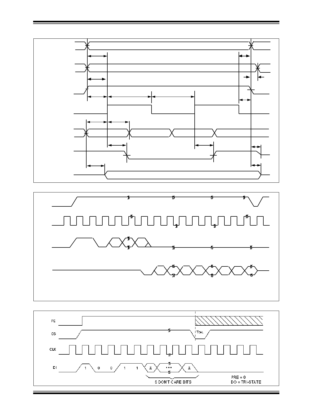
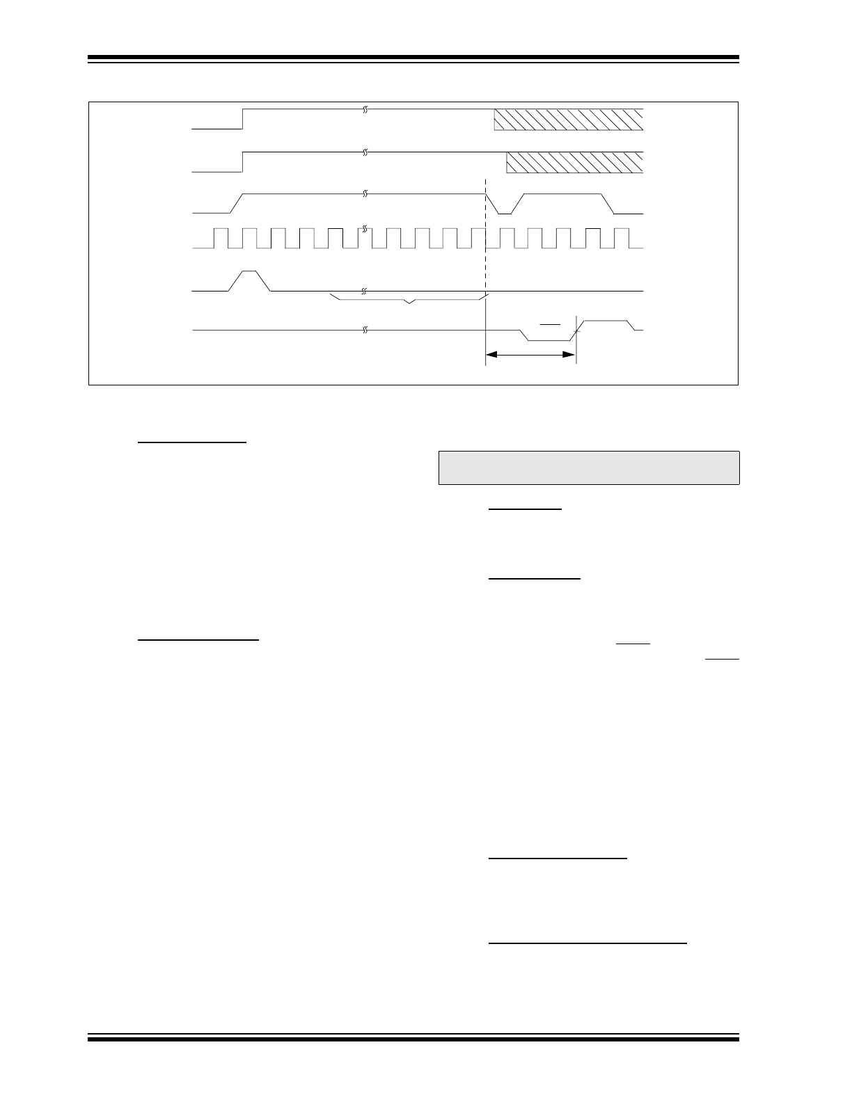
FIGURE 2-1:
SYNCHRONOUS DATA TIMING
FIGURE 2-2:
READ TIMING
FIGURE 2-3:
EWEN TIMING
CLK
STATUS VALID
V
IH
V
IL
CS
T
CSS
T
DIS
T
DIH
T
SV
T
CSH
T
CKH
T
CKL
T
PD
T
CZ
T
CZ
T
PD
V
IH
V
IL
DI
V
IH
V
IL
DO
(READ)
V
OH
V
OL
DO
(PROGRAM)
V
OH
V
OL
T
PRES
PRE
V
IH
V
IL
PE
V
IH
V
IL
T
PES
T
PREH
T
PEH
CLK
CS
T
CSL
A2
• • •
A0
0
1 1
DI
DO
* The memory automatically cycles to the next register.
Tri-State is a registered trademark of National Semiconductor.
D15
• • •
D0
0
D15*
• • •
D0
D15*
TRI-STATE
PRE = 0
PE = X
• • •
2004 Microchip Technology Inc.
DS11181E-page 7
93LCS56/66
FIGURE 2-4:
EWDS TIMING
FIGURE 2-5:
WRITE TIMING
FIGURE 2-6:
WRAL TIMING
CLK
CS
T
CSL
0 0
1
DI
0 0
PRE = 0
PE = X
DO = TRI-STATE
† † †
X
X
6 DON'T CARE BITS
CLK
CS
T
CSL
0
1
DI
† † †
BUSY
D0
1
A0
† † †
D15
READY
T
WC
DO
TRI-STATE
A7
PE
PRE = 0
† Address bit A7 becomes a "don't care" for 93LCS56.
CLK
CS
T
CSL
0
1
DI
• • •
BUSY
D0
X
0
X
• • •
D15
READY
T
WL
DO
0
1
TRI-STATE
PE
Guaranteed at V
CC
= 4.5V to 6.0V
Protect Register must be cleared
PRE = 0
6 DON'T CARE BITS
TRISTATE
93LCS56/66
DS11181E-page 8
2004 Microchip Technology Inc.
FIGURE 2-7:
ERASE TIMING
FIGURE 2-8:
ERAL TIMING
FIGURE 2-9:
PRREAD TIMING
CLK
CS
T
CSL
1
DI
A7
BUSY
A0
† † †
READY
T
WC
DO
1
1
CHECK STATUS
STANDBY
T
CZ
TRI-STATE
T
SV
TRI-STATE
PE
PRE = 0
† Address bit A7 is a "don't care" for 93LCS56.
CLK
CS
T
CSL
0
DI
0
BUSY
0
READY
T
EC
DO
1
1
CHECK STATUS
STANDBY
T
CZ
TRI-STATE
T
SV
TRI-STATE
Guarantee at V
CC
= 4.5V to 6.0V
Protect Register must be cleared
PE
PRE = 0
† † †
X
X
6 DON'T CARE BITS
CLK
CS
T
CSL
1
DI
X
† † †
DO
1
0
PRE
X
A6
† † †
A0
0
A7
† X †
PE = X
† Address bit A7 is a "don't care" for 93LCS56.
8 DON'T CARE BITS
2004 Microchip Technology Inc.
DS11181E-page 9
93LCS56/66
FIGURE 2-10: PREN TIMING
FIGURE 2-11: PRCLEAR TIMING
FIGURE 2-12: PRWRITE TIMING
CLK
CS
T
CSL
1
DI
X
† † †
0
1
PE
X
DO = TRI-STATE
A EWEN cycle must precede a PREN cycle.
PRE
0
1
6 DON'T CARE BITS
CLK
CS
T
CSL
1
DI
BUSY
• • •
READY
T
WC
DO
1
TRI-STATE
PE
PRE
1
1
1
1
1
1
A PREN cycle must immediately precede a PRCLEAR cycle.
8 BITS OF "1"
CLK
CS
T
CSL
0
DI
BUSY
READY
T
WC
DO
1
PE
PRE
1
A7
• • •
A0
Protect Register MUST be cleared before a PRWRITE cycle.
A PREN cycle must immediately precede a PRWRITE cycle.
Address bit A7 is a "don't care" for 93LCS56.
93LCS56/66
DS11181E-page 10
2004 Microchip Technology Inc.
FIGURE 2-13: PRDS TIMING
CLK
CS
T
CSL
0
DI
BUSY
• • •
READY
T
WC
DO
1
ONE TIME ONLY instruction. A PREN cycle must immediately precede a PRDS cycle.
PE
PRE
0
0
0
0
0
0
8 BITS OF "0"
3.0
PIN DESCRIPTION
3.1
Chip Select (CS)
A HIGH level selects the device. A LOW level deselects
the device and forces it into standby mode. However, a
programming cycle which is already initiated and/or in
progress will be completed, regardless of the CS input
signal. If CS is brought LOW during a program cycle,
the device will go into standby mode as soon as the
programming cycle is completed.
CS must be LOW for 250 ns minimum (T
CSL
) between
consecutive instructions. If CS is LOW, the internal
control logic is held in a RESET status.
3.2
Serial Clock (CLK)
The Serial Clock is used to synchronize the communi-
cation between a master device and the 93LCS56/66.
Opcode, address, and data bits are clocked in on the
positive edge of CLK. Data bits are also clocked out on
the positive edge of CLK.
CLK can be stopped anywhere in the transmission
sequence (at HIGH or LOW level) and can be contin-
ued anytime with respect to clock HIGH time (TCDD)
and clock LOW time (T
CKL
). This gives the controlling
master freedom in preparing opcode, address, and
data.
CLK is a “Don't Care” if CS is LOW (device deselected).
If CS is HIGH, but START condition has not been
detected, any number of clock cycles can be received
by the device without changing its status (i.e., waiting
for START condition).
CLK cycles are not required during the self-timed
WRITE (i.e., auto ERASE/WRITE) cycle.
After detection of a start condition the specified number
of clock cycles (respectively LOW to HIGH transitions
of CLK) must be provided. These clock cycles are
required to clock in all required opcode, address, and
data bits before an instruction is executed (see instruc-
tion set truth table). CLK and DI then become don't care
inputs waiting for a new start condition to be detected.
3.3
Data In (DI)
Data In is used to clock in a START bit, opcode,
address, and data synchronously with the CLK input.
3.4
Data Out (DO)
Data Out is used in the READ and PRREAD mode to
output data synchronously with the CLK input (T
PD
after the positive edge of CLK).
This pin also provides READY/BUSY status informa-
tion during ERASE and WRITE cycles. READY/BUSY
status information is available on the DO pin if CS is
brought HIGH after held LOW for minimum chip select
low time (T
CSL
) and an ERASE or WRITE operation
has been initiated.
The status signal is not available on DO, if CS is held
LOW or HIGH during the entire WRITE or ERASE
cycle. In all other cases DO is in the HIGH-Z mode. If
status is checked after the WRITE/ERASE cycle, a
pull-up resistor on DO is required to read the READY
signal.
3.5
Program Enable (PE)
This pin should be held HIGH in the programming
mode or when executing the Protect Register program-
ming instructions.
3.6
Protect Register Enable (PRE)
This pin should be held HIGH when executing all Pro-
tect Register instructions. Otherwise, it must be held
LOW for normal operations.
Note:
CS must go LOW between consecutive
instructions.
2004 Microchip Technology Inc.
DS11181E-page 1
FEATURES
• Single supply with programming operation down
to 2.5V
• Low power CMOS technology
- 1 mA active current typical
- 5
µ
A standby current (typical) at 3.0V
• x16 memory organization
- 128x16 (93LCS56)
- 256x16 (93LCS66)
• Software write protection of user defined memory
space
• Self timed erase and write cycles
• Automatic ERAL before WRAL
• Power on/off data protection
• Industry standard 3-wire serial I/O
• Device status signal during E/W
• Sequential READ function
• 1,000,000 E/W cycles guaranteed
• Data retention > 200 years
• 8-pin PDIP/SOIC and 14-pin SOIC packages
• Temperature ranges supported
- Commercial (C):
0°C to +70°C
- Industrial (I):
-40°C to +85°C
BLOCK DIAGRAM
DESCRIPTION
The Microchip Technology Inc. 93LCS56/66 are low volt-
age Serial Electrically Erasable PROMs with memory
capacities of 2K bits/4K bits respectively. A write protect
register is included in order to provide a user defined
region of write protected memory. All memory locations
greater than or equal to the address placed in the write
protect register will be protected from any attempted write
or erase operation. It is also possible to protect the
address in the write protect register permanently by using
a one time only instruction (PRDS). Any attempt to alter
data in a register whose address is equal to or greater
than the address stored in the protect register will be
aborted. Advanced CMOS technology makes this device
ideal for low power non-volatile memory applications.
MEMORY
ARRAY
ADDRESS
DECODER
V
CC
V
SS
DATA REGISTER
DO
MODE
DECODE
LOGIC
CLOCK
GENERATOR
OUTPUT
BUFFER
DI
CS
CLK
PRE
ADDRESS
COUNTER
PE
93LCS56/66
2K/4K 2.5V Microwire
®
Serial EEPROM with Software Write Protect
PACKAGE TYPES
93LCS56
93LCS66
93LCS56
93LCS66
93LCS56
93LCS66
SOIC
1
2
3
4
5
6
7
14
13
12
11
10
9
8
NC
V
CC
PRE
NC
PE
V
SS
NC
NC
CS
CLK
NC
DI
DO
NC
SOIC
1
2
3
4
8
7
6
5
V
CC
PRE
PE
V
SS
CS
CLK
DI
DO
1
2
3
4
8
7
6
5
V
CC
PRE
PE
V
SS
CS
CLK
DI
DO
DIP
Microwire is a registered trademark of National Semiconductor Incorporated.
Obsolete Device
93LCS56/66
DS11181E-page 2
2004 Microchip Technology Inc.
1.0
ELECTRICAL CHARACTERISTICS
1.1
Maximum Ratings*
V
CC
...................................................................................7.0V
All inputs and outputs w.r.t. V
SS
............... -0.6V to V
CC
+1.0V
Storage temperature .....................................-65°C to +150°C
Ambient temp. with power applied ................-65°C to +125°C
Soldering temperature of leads (10 seconds) ............. +300°C
ESD protection on all pins................................................4 kV
*Notice: Stresses above those listed under “Maximum ratings”
may cause permanent damage to the device. This is a stress rat-
ing only and functional operation of the device at those or any
other conditions above those indicated in the operational listings
of this specification is not implied. Exposure to maximum rating
conditions for extended periods may affect device reliability.
TABLE 1-1:
PIN FUNCTION TABLE
Name
Function
CS
Chip Select
CLK
Serial Data Clock
DI
Serial Data Input
DO
Serial Data Output
V
SS
Ground
PE
Program Enable
PRE
Protect Register Enable
V
CC
Power Supply
TABLE 1-2:
DC AND AC ELECTRICAL CHARACTERISTICS
V
CC
= +2.5V to +6.0V
Commercial(C): Tamb = 0°C to +70°C
Industrial (I):
Tamb = -40°C to +85°C
Parameter
Symbol
Min
Max
Units
Conditions
High level input voltage
V
IH
2.0
V
CC
+1
V
V
CC
≥
2.5V
Low level input voltage
V
IL
-0.3
0.8
V
V
CC
≥
2.5V
Low level output voltage
V
OL
1
—
0.4
V
I
OL
= 2.1 mA; V
CC
= 4.5V
V
OL
2
—
0.2
V
I
OL
= 100
µ
A; V
CC
= 2.5V
High level output voltage
V
OH
1
2.4
—
V
I
OH
= -400
µ
A; V
CC
= 4.5V
V
OH
2
V
CC
-0.2
—
V
I
OH
= -100
µ
A; V
CC
= 2.5V
Input leakage current
I
LI
-10
10
µ
A
V
IN
= 0.1V to V
CC
Output leakage current
I
LO
-10
10
µ
A
V
OUT
= 0.1V to Vcc
Pin capacitance
(all inputs/outputs)
C
IN
, C
OUT
—
7
pF
V
IN
/V
OUT
= 0V (Note 1 & 2)
Tamb = +25°C; F
CLK
= 1 MHz
Operating current
I
CC
Write
—
3
mA
F
CLK
= 2 MHz; V
CC
= 3.0V (Note 2)
I
CC
Read
—
1
500
mA
µ
A
F
CLK
= 2 MHz; V
CC
= 6.0V
F
CLK
= 1 MHz; V
CC
= 3.0V
Standby current
I
CCS
—
100
30
µ
A
µ
A
CLK = CS = 0V; V
CC
= 6.0V
CLK = CS = 0V; V
CC
= 3.0V
DI = PE = PRE = V
SS
Clock frequency
F
CLK
—
2
1
MHz
MHz
V
CC
≥
4.5V
V
CC
< 4.5V
Clock high time
T
CKH
250
—
ns
Clock low time
T
CKL
250
—
ns
Chip select setup time
T
CSS
50
—
ns
Relative to CLK
Chip select hold time
T
CSH
0
—
ns
Relative to CLK
Chip select low time
T
CSL
250
—
ns
PRE setup time
T
PRES
100
—
ns
Relative to CLK
PE setup time
T
PES
100
—
ns
Relative to CLK
PRE hold time
T
PREH
0
—
ns
Relative to CLK
PE hold time
T
PEH
500
—
ns
Relative to CLK
Data input setup time
T
DIS
100
—
ns
Relative to CLK
Data input hold time
T
DIH
100
—
ns
Relative to CLK
Data output delay time
T
PD
—
400
ns
CL=100 pF
Data output disable time
T
CZ
—
100
ns
CL=100 pF (Note 2)
Note 1: This parameter is tested at Tamb = 25°C and F
CLK
= 1 MHz.
2: This parameter is periodically sampled and not 100% tested.
2004 Microchip Technology Inc.
DS11181E-page 3
93LCS56/66
TABLE 1-3:
INSTRUCTION SET FOR 93LCS56*/66
Status valid time
T
SV
500
ns
CL=100 pF
Program cycle time
T
WC
10
ms
ERASE/WRITE mode (Note 3)
T
EC
15
ms
ERAL mode
T
WL
30
ms
WRAL mode
Endurance
—
1M
—
cycles
25°C, Vcc = 5.0V, Block Mode
(Note 4)
3: Typical program cycle time is 4 ms per word.
4: This parameter is not tested but guaranteed by characterization. For endurance estimates in a specific appli-
cation, please consult the Total Endurance Model which can be obtained on our BBS or website.
93LCS56/66 (x 16 organization)
Instruction SB Opcode
Address
Data In
Data Out
PRE
PE
Comments
READ
1
10
A7 - A0
—
D15-D0
0
X
Reads data stored in memory, start-
ing at specified address (.Note).
EWEN
1
00
11XXXXXX
—
High-Z
0
1
Erase/Write Enable must precede all
programming modes.
ERASE
1
11
A7 - A0
—
(RDY/
BSY)
1
Erase data at specified address
location if address is unprotected
(Note).
ERAL
1
00
10XXXXXX
—
(RDY/
BSY)
0
1
Erase all registers to “FF”. Valid only
when Protect Register is cleared.
WRITE
1
01
A7 - A0*
D15 - D0
(RDY/
BSY)
0
1
Writes register if address is unpro-
tected.
WRAL
1
00
01XXXXXX
D15 - D0
(RDY/
BSY)
0
1
Writes all registers. Valid only when
Protect Register is cleared.
EWDS
1
00
00XXXXXX
—
High-Z
0
X
Erase/Write Disable deactivates all
programming instructions.
PRREAD
1
10
XXXXXXXX
—
A7-A0
1
X
Reads address stored in Protect
Register.
PREN
1
00
11XXXXXX
—
High-Z
1
1
Must immediately precede
PRCLEAR, PRWRITE and PRDS
instructions.
PRCLEAR
1
11
11111111
—
(RDY/
BSY)
1
1
Clears the Protect Register such that
all data are NOT write-protected.
PRWRITE
1
01
A7 - A0*
—
(RDY/
BSY)
1
1
Programs address into Protect Reg-
ister. Thereafter, memory addresses
greater than or equal to the address
in Protect Register are write-pro-
tected.
PRDS
1
00
00000000
—
(RDY/
BSY)
1
1
ONE TIME ONLY instruction after
which the address in the Protect
Register cannot be altered.
Note:
Address A7 bit is a “don’t care” on 93LCS56.
TABLE 1-2:
DC AND AC ELECTRICAL CHARACTERISTICS
V
CC
= +2.5V to +6.0V
Commercial(C): Tamb = 0°C to +70°C
Industrial (I):
Tamb = -40°C to +85°C
Parameter
Symbol
Min
Max
Units
Conditions
(Continued)
93LCS56/66
DS11181E-page 4
2004 Microchip Technology Inc.
2.0
FUNCTIONAL DESCRIPTION
The 93LCS56/66 is organized as 128/256 registers by
16 bits. Instructions, addresses and write data are
clocked into the DI pin on the rising edge of the clock
(CLK). The DO pin is normally held in a high-Z state
except when reading data from the device, or when
checking the ready/busy status during a programming
operation. The ready/busy status can be verified during
an Erase/Write operation by polling the DO pin; DO low
indicates that programming is still in progress, while
DO high indicates the device is ready. The DO will enter
the high-Z state on the falling edge of the CS.
2.1
START Condition
The START bit is detected by the device if CS and DI
are both HIGH with respect to the positive edge of CLK
for the first time.
Before a START condition is detected, CS, CLK, and DI
may change in any combination (except to that of a
START condition), without resulting in any device oper-
ation (READ, WRITE, ERASE, EWEN, EWDS, ERAL,
WRAL, PRREAD, PREN, PRCLEAR, PRWRITE, and
PRDS). As soon as CS is HIGH, the device is no longer
in the standby mode.
An instruction following a START condition will only be
executed if the required amount of opcode, address
and data bits for any particular instruction is clocked in.
After execution of an instruction (i.e., clock in or out of
the last required address or data bit) CLK and DI
become don't care bits until a new start condition is
detected.
2.2
DI/DO
It is possible to connect the Data In and Data Out pins
together. However, with this configuration it is possible
for a “bus conflict” to occur during the “dummy zero”
that precedes the READ operation, if A0 is a logic
HIGH level. Under such a condition the voltage level
seen at Data Out is undefined and will depend upon the
relative impedances of Data Out and the signal source
driving A0. The higher the current sourcing capability of
A0, the higher the voltage at the Data Out pin.
2.3
Data Protection
During power-up, all programming modes of operation
are inhibited until V
CC
has reached a level greater than
1.4V. During power-down, the source data protection
circuitry acts to inhibit all programming modes when
V
CC
has fallen below 1.4V.
The EWEN and EWDS commands give additional pro-
tection against accidentally programming during nor-
mal operation.
After power-up, the device is automatically in the
EWDS mode. Therefore, an EWEN instruction must be
performed before any ERASE or WRITE instruction
can be executed.
2.4
READ
The READ instruction outputs the serial data of the
addressed memory location on the DO pin. A dummy
zero bit precedes the 16 bit output string. The output
data bits will toggle on the rising edge of the CLK and
are stable after the specified time delay (T
PD
). Sequen-
tial read is possible when CS is held high. The memory
data will automatically cycle to the next register and
output sequentially.
2.5
Erase/Write Enable and Disable
(EWEN, EWDS)
The 93LCS56/66 powers up in the Erase/Write Disable
(EWDS) state. All programming modes must be pre-
ceded by an Erase/Write Enable (EWEN) instruction.
The PE pin MUST be held “high” while loading the
EWEN instruction. Once the EWEN instruction is exe-
cuted, programming remains enabled until an EWDS
instruction is executed or V
CC
is removed from the
device. To protect against accidental data disturb, the
EWDS instruction can be used to disable all Erase/
Write functions and should follow all programming
operations. Execution of a READ instruction is inde-
pendent of both the EWEN and EWDS instructions.
2.6
ERASE
The ERASE instruction forces all data bits of the spec-
ified address to the logical “1” state. CS is brought low
following the loading of the last address bit. This falling
edge of the CS pin initiates the self-timed programming
cycle. The PE pin MUST be latched “high” during load-
ing the ERASE instruction but becomes a “don't care”
after loading the instruction.
The DO pin indicates the READY/BUSY status of the
device if CS is brought high after a minimum of 250 ns
low (T
CLS
). DO at logical “0” indicates that program-
ming is still in progress. DO at logical “1” indicates that
the register at the specified address has been erased
and the device is ready for another instruction. ERASE
instruction is valid if specified address is unprotected.
The ERASE cycle takes 4 ms per word typical.
2.7
WRITE
The WRITE instruction is followed by 16 bits of data
which are written into the specified address. After the
last data bit is put on the DI pin, CS must be brought
low before the next rising edge of the CLK clock. Both
CS and CLK must be low to initiate the self-timed auto-
erase and programming cycle. The PE pin MUST be
latched “high” while loading the WRITE instruction but
becomes a “don't care” thereafter.
2004 Microchip Technology Inc.
DS11181E-page 5
93LCS56/66
The DO pin indicates the READY/BUSY status of the
device if CS is brought high after a minimum of 250 ns
(T
CSL
) and before the entire write cycle is complete. DO
at logical “0” indicates that programming is still in
progress. DO at logical “1” indicates that the register at
the specified address has been written with the data
specified and the device is ready for another instruc-
tion. WRITE instruction is valid only if specified address
is unprotected.
The WRITE cycle takes 4 ms per word typical.
2.8
Erase All (ERAL)
The ERAL instruction will erase the entire memory
array to the logical “1”. The ERAL cycle is identical to
the ERASE cycle except for the different opcode. The
ERAL cycle is completely self-timed and commences
at the falling edge of the CS. PE pin MUST be held
“high” while loading the instruction but becomes “don't
care” thereafter. Clocking of the CLK pin is not neces-
sary after the device has entered the self clocking
mode. The ERAL instruction is guaranteed at V
CC
= 4.5
to 6V and valid only when Protect Register is cleared.
The DO pin indicates the READY/BUSY status of the
device if CS is brought high after a minimum of 250 ns
low (T
CSL
) and before the entire write cycle is complete.
The ERAL cycle takes 15 ms maximum (8 ms typical).
2.9
Write All (WRAL)
The WRAL instruction will write the entire memory
array with the data specified in the command. The
WRAL cycle is completely self-timed and commences
at the falling edge of the CS. PE pin MUST be held
“high” while loading the instruction but becomes “don't
care” thereafter. Clocking of the CLK pin is not neces-
sary after the device has entered the self clocking
mode. The WRAL command does include an automatic
ERAL cycle for the device. Therefore, the WRAL
instruction does not require an ERAL instruction but the
chip must be in the EWEN status. The WRAL instruc-
tion is guaranteed at V
CC
= 4.5 to 6V and valid only
when Protect Register is cleared.
The DO pin indicates the READY/BUSY status of the
device if CS is brought high after a minimum of 250 ns
low (T
CSL
).
The WRAL cycle takes 30 ms maximum (16 ms typi-
cal).
Note:
In order to execute either READ, EWEN,
ERAL, WRITE, WRAL, or EWDS instruc-
tions, the Protect Register Enable (PRE)
pin must be held LOW.
2.10
Protect Register Read (PRREAD)
The Protect Register Read (PRREAD) instruction out-
puts the address stored in the Protect Register on the
DO pin. The PRE pin MUST be held HIGH when load-
ing the instruction and remains HIGH until CS goes
LOW. A dummy zero bit precedes the 8-bit output
string. The output data bits in the memory Protect Reg-
ister will toggle on the rising edge of the CLK as in the
READ mode.
2.11
Protect Register Enable (PREN)
The Protect Register Enable (PREN) instruction is
used to enable the PRCLEAR, PRWRITE, and PRDS
modes. Before the PREN mode can be entered, the
device must be in the EWEN mode. Both PRE and PE
pins MUST be held “high” while loading the instruction.
The PREN instruction MUST immediately precede a
PRCLEAR, PRWRITE, or PRDS instruction.
2.12
Protect Register Clear (PRCLEAR)
The Protect Register Clear (PRCLEAR) instruction
clears the address stored in the Protect Register and,
therefore, enables all registers for programming
instructions such as ERASE, ERAL, WRITE, and
WRAL. The PRE and PE pin MUST be held HIGH
when loading the instruction. Thereafter, PRE and PE
pins become “don't care”. A PREN instruction must
immediately precede a PRCLEAR instruction.
2.13
Protect Register Write (PRWRITE)
The Protect Register Write (PRWRITE) instruction
writes into the Protect Register the address of the first
register to be protected. After this instruction is exe-
cuted, all registers whose memory addresses are
greater than or equal to the address pointer specified in
the Protect register are protected from any program-
ming instructions. Note that a PREN instruction must
be executed before a PRWRITE instruction and, the
Protect Register must be cleared (by a PRCLEAR
instruction) before executing the PRWRITE instruction.
The PRE and PE pins MUST be held HIGH while load-
ing PRWRITE instruction. After the instruction is
loaded, they become “don't care”.
2.14
Protect Register Disable (PRDS)
The Protect Register Disable (PRDS) instruction is a
ONE TIME ONLY instruction to permanently set the
address specified in the Protect Register. Any attempts
to change the address pointer will be aborted. The PRE
and PE pins MUST be held HIGH while loading PRDS
instruction. After the instruction is loaded, they become
“don't care”. Note that a PREN instruction must be exe-
cuted before a PRDS instruction.
93LCS56/66
DS11181E-page 6
2004 Microchip Technology Inc.
FIGURE 2-1:
SYNCHRONOUS DATA TIMING
FIGURE 2-2:
READ TIMING
FIGURE 2-3:
EWEN TIMING
CLK
STATUS VALID
V
IH
V
IL
CS
T
CSS
T
DIS
T
DIH
T
SV
T
CSH
T
CKH
T
CKL
T
PD
T
CZ
T
CZ
T
PD
V
IH
V
IL
DI
V
IH
V
IL
DO
(READ)
V
OH
V
OL
DO
(PROGRAM)
V
OH
V
OL
T
PRES
PRE
V
IH
V
IL
PE
V
IH
V
IL
T
PES
T
PREH
T
PEH
CLK
CS
T
CSL
A2
• • •
A0
0
1 1
DI
DO
* The memory automatically cycles to the next register.
Tri-State is a registered trademark of National Semiconductor.
D15
• • •
D0
0
D15*
• • •
D0
D15*
TRI-STATE
PRE = 0
PE = X
• • •
2004 Microchip Technology Inc.
DS11181E-page 7
93LCS56/66
FIGURE 2-4:
EWDS TIMING
FIGURE 2-5:
WRITE TIMING
FIGURE 2-6:
WRAL TIMING
CLK
CS
T
CSL
0 0
1
DI
0 0
PRE = 0
PE = X
DO = TRI-STATE
† † †
X
X
6 DON'T CARE BITS
CLK
CS
T
CSL
0
1
DI
† † †
BUSY
D0
1
A0
† † †
D15
READY
T
WC
DO
TRI-STATE
A7
PE
PRE = 0
† Address bit A7 becomes a "don't care" for 93LCS56.
CLK
CS
T
CSL
0
1
DI
• • •
BUSY
D0
X
0
X
• • •
D15
READY
T
WL
DO
0
1
TRI-STATE
PE
Guaranteed at V
CC
= 4.5V to 6.0V
Protect Register must be cleared
PRE = 0
6 DON'T CARE BITS
TRISTATE
93LCS56/66
DS11181E-page 8
2004 Microchip Technology Inc.
FIGURE 2-7:
ERASE TIMING
FIGURE 2-8:
ERAL TIMING
FIGURE 2-9:
PRREAD TIMING
CLK
CS
T
CSL
1
DI
A7
BUSY
A0
† † †
READY
T
WC
DO
1
1
CHECK STATUS
STANDBY
T
CZ
TRI-STATE
T
SV
TRI-STATE
PE
PRE = 0
† Address bit A7 is a "don't care" for 93LCS56.
CLK
CS
T
CSL
0
DI
0
BUSY
0
READY
T
EC
DO
1
1
CHECK STATUS
STANDBY
T
CZ
TRI-STATE
T
SV
TRI-STATE
Guarantee at V
CC
= 4.5V to 6.0V
Protect Register must be cleared
PE
PRE = 0
† † †
X
X
6 DON'T CARE BITS
CLK
CS
T
CSL
1
DI
X
† † †
DO
1
0
PRE
X
A6
† † †
A0
0
A7
† X †
PE = X
† Address bit A7 is a "don't care" for 93LCS56.
8 DON'T CARE BITS
2004 Microchip Technology Inc.
DS11181E-page 9
93LCS56/66
FIGURE 2-10: PREN TIMING
FIGURE 2-11: PRCLEAR TIMING
FIGURE 2-12: PRWRITE TIMING
CLK
CS
T
CSL
1
DI
X
† † †
0
1
PE
X
DO = TRI-STATE
A EWEN cycle must precede a PREN cycle.
PRE
0
1
6 DON'T CARE BITS
CLK
CS
T
CSL
1
DI
BUSY
• • •
READY
T
WC
DO
1
TRI-STATE
PE
PRE
1
1
1
1
1
1
A PREN cycle must immediately precede a PRCLEAR cycle.
8 BITS OF "1"
CLK
CS
T
CSL
0
DI
BUSY
READY
T
WC
DO
1
PE
PRE
1
A7
• • •
A0
Protect Register MUST be cleared before a PRWRITE cycle.
A PREN cycle must immediately precede a PRWRITE cycle.
Address bit A7 is a "don't care" for 93LCS56.
93LCS56/66
DS11181E-page 10
2004 Microchip Technology Inc.
FIGURE 2-13: PRDS TIMING
CLK
CS
T
CSL
0
DI
BUSY
• • •
READY
T
WC
DO
1
ONE TIME ONLY instruction. A PREN cycle must immediately precede a PRDS cycle.
PE
PRE
0
0
0
0
0
0
8 BITS OF "0"
3.0
PIN DESCRIPTION
3.1
Chip Select (CS)
A HIGH level selects the device. A LOW level deselects
the device and forces it into standby mode. However, a
programming cycle which is already initiated and/or in
progress will be completed, regardless of the CS input
signal. If CS is brought LOW during a program cycle,
the device will go into standby mode as soon as the
programming cycle is completed.
CS must be LOW for 250 ns minimum (T
CSL
) between
consecutive instructions. If CS is LOW, the internal
control logic is held in a RESET status.
3.2
Serial Clock (CLK)
The Serial Clock is used to synchronize the communi-
cation between a master device and the 93LCS56/66.
Opcode, address, and data bits are clocked in on the
positive edge of CLK. Data bits are also clocked out on
the positive edge of CLK.
CLK can be stopped anywhere in the transmission
sequence (at HIGH or LOW level) and can be contin-
ued anytime with respect to clock HIGH time (TCDD)
and clock LOW time (T
CKL
). This gives the controlling
master freedom in preparing opcode, address, and
data.
CLK is a “Don't Care” if CS is LOW (device deselected).
If CS is HIGH, but START condition has not been
detected, any number of clock cycles can be received
by the device without changing its status (i.e., waiting
for START condition).
CLK cycles are not required during the self-timed
WRITE (i.e., auto ERASE/WRITE) cycle.
After detection of a start condition the specified number
of clock cycles (respectively LOW to HIGH transitions
of CLK) must be provided. These clock cycles are
required to clock in all required opcode, address, and
data bits before an instruction is executed (see instruc-
tion set truth table). CLK and DI then become don't care
inputs waiting for a new start condition to be detected.
3.3
Data In (DI)
Data In is used to clock in a START bit, opcode,
address, and data synchronously with the CLK input.
3.4
Data Out (DO)
Data Out is used in the READ and PRREAD mode to
output data synchronously with the CLK input (T
PD
after the positive edge of CLK).
This pin also provides READY/BUSY status informa-
tion during ERASE and WRITE cycles. READY/BUSY
status information is available on the DO pin if CS is
brought HIGH after held LOW for minimum chip select
low time (T
CSL
) and an ERASE or WRITE operation
has been initiated.
The status signal is not available on DO, if CS is held
LOW or HIGH during the entire WRITE or ERASE
cycle. In all other cases DO is in the HIGH-Z mode. If
status is checked after the WRITE/ERASE cycle, a
pull-up resistor on DO is required to read the READY
signal.
3.5
Program Enable (PE)
This pin should be held HIGH in the programming
mode or when executing the Protect Register program-
ming instructions.
3.6
Protect Register Enable (PRE)
This pin should be held HIGH when executing all Pro-
tect Register instructions. Otherwise, it must be held
LOW for normal operations.
Note:
CS must go LOW between consecutive
instructions.