
2004 Microchip Technology Inc.
DS11126H-page 1
FEATURES
• Fast Read Access Time—150 ns
• CMOS Technology for Low Power Dissipation
- 30 mA Active
- 100
µ
A Standby
• Fast Byte Write Time—200
µ
s or 1 ms
• Data Retention >200 years
• Endurance - Minimum 10
4
Erase/Write Cycles
- Automatic Write Operation
- Internal Control Timer
- Auto-Clear Before Write Operation
- On-Chip Address and Data Latches
• Data Polling
• Chip Clear Operation
• Enhanced Data Protection
- V
CC
Detector
- Pulse Filter
- Write Inhibit
• 5-Volt-Only Operation
• Organized 512x8 JEDEC standard pinout
- 24-pin Dual-In-Line Package
- 32-pin PLCC Package
• Available for Extended Temperature Ranges:
- Commercial: 0°C to +70°C
- Industrial: -40°C to +85°C
DESCRIPTION
The Microchip Technology Inc. 28C04A is a CMOS 4K
non-volatile electrically Erasable and Programmable
Read Only Memory (EEPROM). The 28C04A is
accessed like a static RAM for the read or write cycles
without the need of external components. During a
“byte write”, the address and data are latched inter-
nally, freeing the microprocessor address and data bus
for other operations. Following the initiation of write
cycle, the device will go to a busy state and automati-
cally clear and write the latched data using an internal
control timer. To determine when a write cycle is com-
plete, the 28C04A uses Data polling. Data polling
allows the user to read the location last written to when
the write operation is complete. CMOS design and pro-
cessing enables this part to be used in systems where
reduced power consumption and reliability are
required. A complete family of packages is offered to
provide the utmost flexibility in applications.
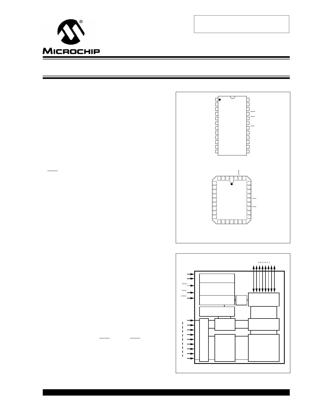
PACKAGE TYPES
BLOCK DIAGRAM
• 1
2
3
4
5
6
7
8
9
10
11
12
24
23
22
21
20
19
18
17
16
15
14
13
A7
A6
A5
A4
A3
A2
A1
A0
I/O0
I/O1
I/O2
V
Vcc
A8
NC
WE
OE
NC
CE
I/O7
I/O6
I/O5
I/O4
I/O3
SS
A6
A5
A4
A3
A2
A1
A0
NC
I/O0
A8
NC
NC
NC
OE
NC
CE
I/O7
I/O6
A7
NC
NC
NU
Vc
c
W
E
NC
I/O1
I/O2
Vss
NU
I/O3
I/O4
I/O5
14
15
16
17
18
19
20
4
3
2
1
32
31
30
29
28
27
26
25
24
23
22
21
5
6
7
8
9
10
11
12
13
DIP
PLCC
28
C
04A
• Pin 1 indicator on PLCC on top of package
28C
0
4
A
I/O0
I/O7
Input/Output
Buffers
Chip Enable/
Output Enable
Control Logic
CE
OE
Data Protection
Circuitry
A8
Y Gating
4K bit
Cell Matrix
X
Decoder
Y
Decoder
A0
Data
Poll
Auto Erase/Write
Timing
V
CC
V
SS
WE
L
a
t
c
h
e
s
Program Voltage
Generation
28C04A
4K (512 x 8) CMOS EEPROM
Obsolete Device
28C04A
DS11126H-page 2
2004 Microchip Technology Inc.
1.0
ELECTRICAL CHARACTERISTICS
1.1
MAXIMUM RATINGS*
V
CC
and input voltages w.r.t. V
SS
....... -0.6V to + 6.25V
Voltage on OE w.r.t. V
SS
...................... -0.6V to +13.5V
Output Voltage w.r.t. V
SS
.................-0.6V to V
CC
+0.6V
Storage temperature ..........................-65°C to +125°C
Ambient temp. with power applied .......-50°C to +95°C
*Notice: Stresses above those listed under “Maximum Ratings”
may cause permanent damage to the device. This is a stress rat-
ing only and functional operation of the device at those or any
other conditions above those indicated in the operation listings of
this specification is not implied. Exposure to maximum rating con-
ditions for extended periods may affect device reliability.
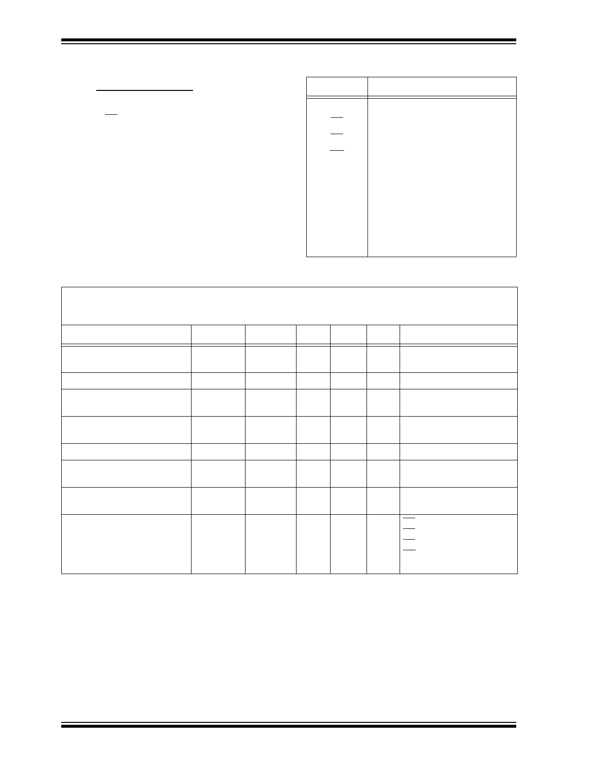
TABLE 1-1:
PIN FUNCTION TABLE
Name
Function
A0 - A8
Address Inputs
CE
Chip Enable
OE
Output Enable
WE
Write Enable
I/O0 - I/O7
Data Inputs/Outputs
V
CC
+5V Power Supply
V
SS
Ground
NC
No Connect; No Internal Connection
NU
Not Used; No External Connection is
Allowed
TABLE 1-2:
READ/WRITE OPERATION DC CHARACTERISTICS
V
CC
= +5V
±
10%
Commercial (C): Tamb =
0°C to +70°C
Industrial (I): Tamb = -40°C to +85°C
Parameter
Status
Symbol
Min
Max
Units
Conditions
Input Voltages
Logic ‘1’
Logic ‘0’
V
IH
V
IL
2.0
-0.1
V
CC
+1
0.8
V
V
Input Leakage
I
LI
-10
10
µ
A
V
IN
= -0.1V to V
CC
+1
Input Capacitance
C
IN
10
pF
V
IN
= 0V; Tamb = 25°C;
f = 1 MHz
Output Voltages
Logic ‘1’
Logic ‘0’
V
OH
V
OL
2.4
0.45
V
V
I
OH
= -400
µ
A
I
OL
= 2.1 mA
Output Leakage
I
LO
-10
10
µ
A
V
OUT
= -0.1V
TO
V
CC
+ 0.1V
Output Capacitance
C
OUT
12
pF
V
IN
= 0V; T
AMB
= 25°C;
f = 1 MHz
Power Supply Current, Active
TTL input
I
CC
30
mA
f = 5 MHz (Note 1)
V
CC
= 5.5V
Power Supply Current, Standby
TTL input
TTL input
CMOS input
I
CC
(
S
)
TTL
I
CC
(
S
)
TTL
I
CC
(
S
)
CMOS
2
3
100
mA
mA
µ
A
CE = V
IH
(0°C to +70°C)
CE = V
IH
(-40°C to +85°C)
CE = V
CC
-0.3 to V
CC
+1
OE = V
CC
All inputs equal V
CC
or V
SS
Note 1: AC power supply current above 5 MHz; 1 mA/MHz.
2004 Microchip Technology Inc.
DS11126H-page 3
28C04A
TABLE 1-3:
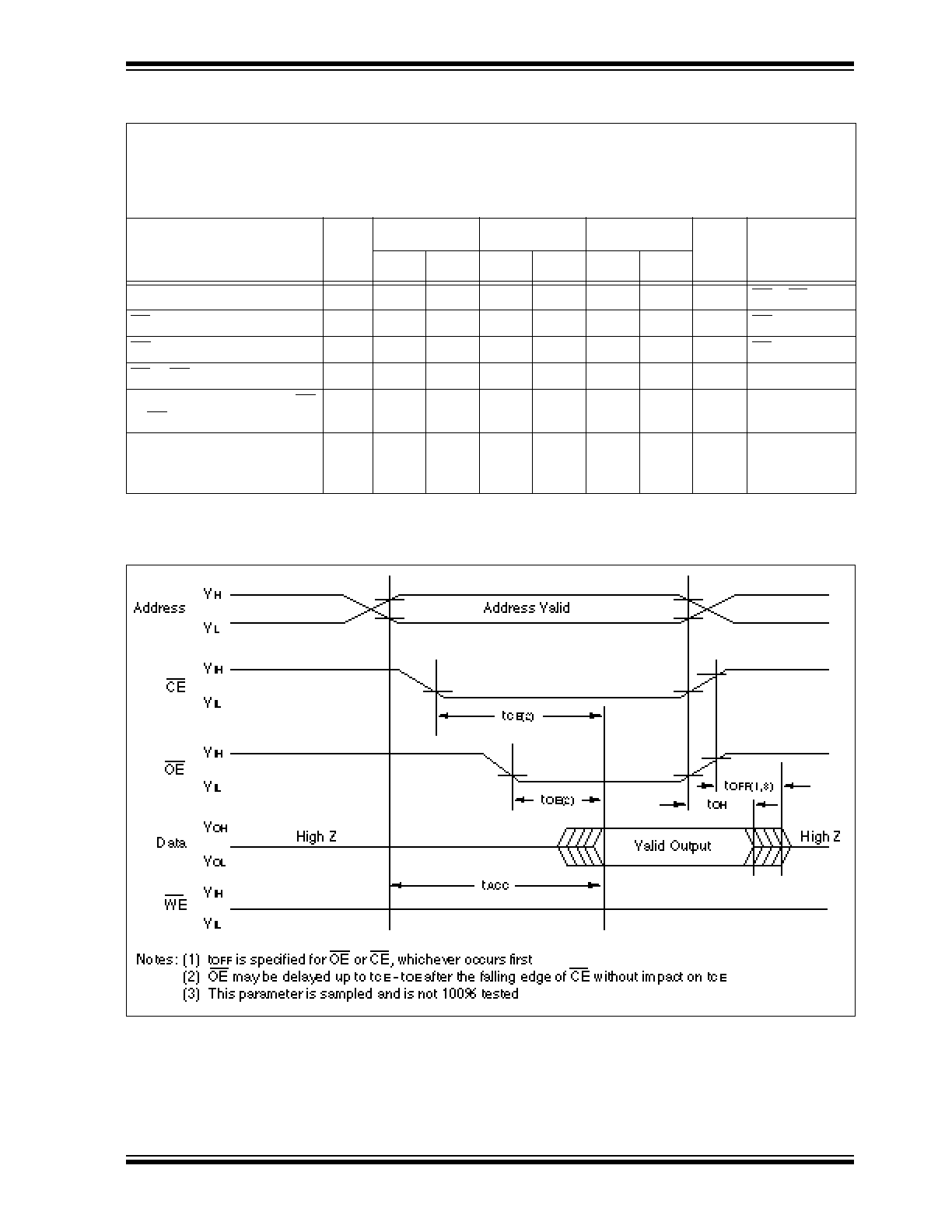
READ OPERATION AC CHARACTERISTICS
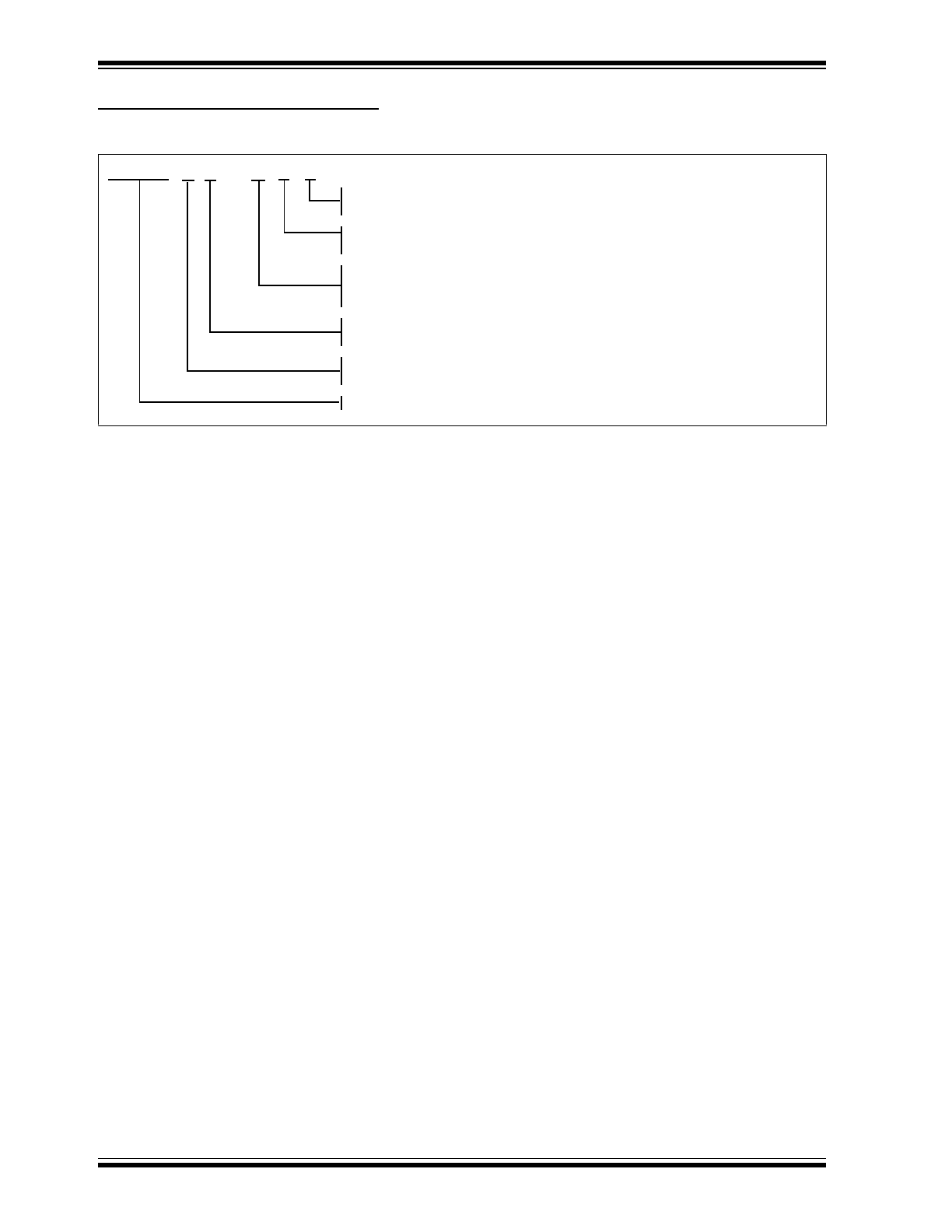
FIGURE 1-1:
READ WAVEFORMS
AC Testing Waveform:
V
IH
= 2.4V; V
IL
= 0.45V; V
OH
= 2.0V; V
OL
= 0.8V
Output Load:
1 TTL Load + 100 pF
Input Rise and Fall Times: 20 ns
Ambient Temperature:
Commercial (C): Tamb =
0°C to +70°C
Industrial
(I):
Tamb =
-40°C to +85°C
Parameter
Sym
28C04A-15
28C04A-20
28C04A-25
Units
Conditions
Min
Max
Min
Max
Min
Max
Address to Output Delay
t
ACC
150
200
250
ns
OE = CE = V
IL
CE to Output Delay
t
CE
150
200
250
ns
OE = V
IL
OE to Output Delay
t
OE
70
80
100
ns
CE = V
IL
CE to OE High Output Float
t
OFF
0
50
0
55
0
70
ns
Output Hold from Address, CE
or OE, whichever occurs first
t
OH
0
0
0
ns
Endurance
—
1M
—
1M
—
1M
—
cycles 25°C, Vcc =
5.0V, Block
Mode (Note)
Note: This parameter is not tested but guaranteed by characterization. For endurance estimates in a specific appli-
cation, please consult the Total Endurance Model which can be obtained on our BBS or website.
28C04A
DS11126H-page 4
2004 Microchip Technology Inc.
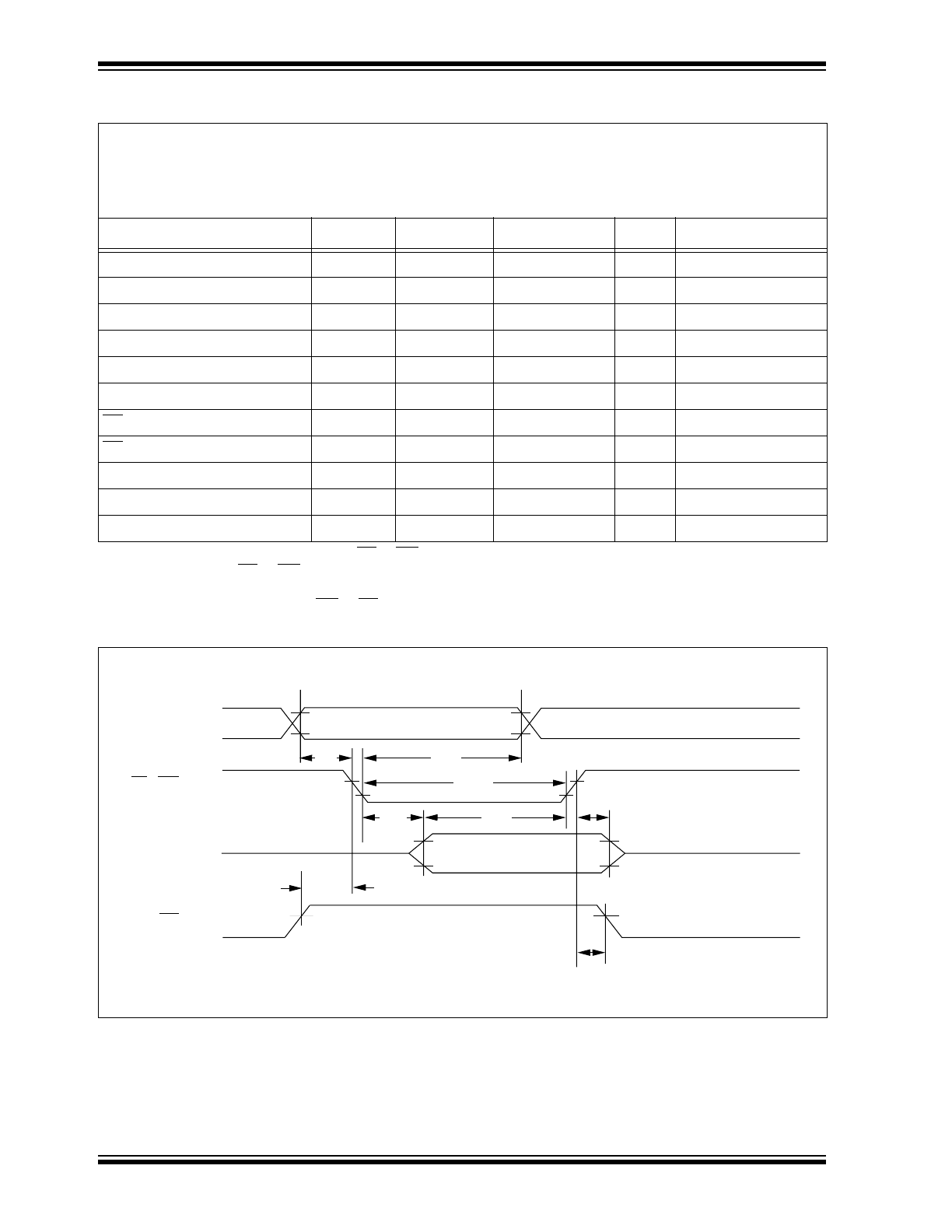
TABLE 1-4:
BYTE WRITE AC CHARACTERISTICS
FIGURE 1-2:
PROGRAMMING WAVEFORMS
AC Testing Waveform:
V
IH
= 2.4V; V
IL
= 0.45V; V
OH
= 2.0V; V
OL
= 0.8V
Output Load:
1 TTL Load + 100 pF
Input Rise/Fall Times:
20 nsec
Ambient Temperature:
Commercial (C): Tamb= 0°C to 70°C
Industrial
(I):
Tamb= -40°C to 85°C
Parameter
Symbol
Min
Max
Units
Remarks
Address Set-Up Time
t
AS
10
ns
Address Hold Time
t
AH
50
ns
Data Set-Up Time
t
DS
50
ns
Data Hold Time
t
DH
10
ns
Write Pulse Width
t
WPL
100
ns
Note 1
Write Pulse High Time
t
WPH
50
ns
OE Hold Time
t
OEH
10
ns
OE Set-Up Time
t
OES
10
ns
Data Valid Time
t
DV
1000
ns
Note 2
Write Cycle Time (28C04A)
t
WC
1
ms
0.5 ms typical
Write Cycle Time (28C04AF)
t
WC
200
µ
s
100
µ
s typical
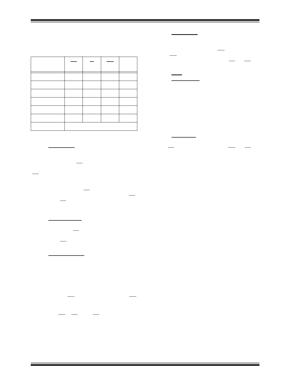
Note 1: A write cycle can be initiated be CE or WE going low, whichever occurs last. The data is latched on the pos-
itive edge of CE or WE, whichever occurs first.
2: Data must be valid within 1000ns max. after a write cycle is initiated and must be stable at least until t
DH
after the positive edge of WE or CE, whichever occurs first.
t
AS
t
AH
t
WPL
t
DS
t
DH
t
OES
t
OEH
t
DV
Address
CE, WE
Data In
OE
V
IH
V
IL
V
IH
V
IL
V
IH
V
IL
V
IH
V
IL
2004 Microchip Technology Inc.
DS11126H-page 5
28C04A
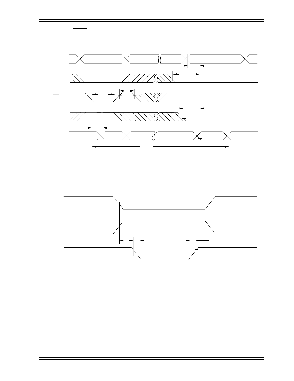
FIGURE 1-3:
DATA POLLING WAVEFORMS
FIGURE 1-4:
CHIP CLEAR WAVEFORMS
Address Valid
Last Written
Address Valid
t
ACC
t
CE
t
WPL
t
WPH
t
DV
t
WC
t
OE
True Data Out
Data In
Valid
V
IH
V
IL
Data
OE
WE
CE
Address
I/O7 Out
V
IH
V
IL
V
IH
V
IL
V
IH
V
IL
V
IH
V
IL
V
H
V
IH
CE
OE
WE
t
S
t
H
t
W
t
S
= = 1
µ
s
t
H
= 10ms
t
W
V
IH
V
IL
V
IH
V
IL
= 12.0V
±
0.5V
V
H
28C04A
DS11126H-page 6
2004 Microchip Technology Inc.
2.0
DEVICE OPERATION
The Microchip Technology Inc. 28C04A has four basic
modes of operation—read, standby, write inhibit, and
byte write—as outlined in the following table.
2.1
Read Mode
The 28C04A has two control functions, both of which
must be logically satisfied in order to obtain data at the
outputs. Chip enable (CE) is the power control and
should be used for device selection. Output Enable
(OE) is the output control and is used to gate data to the
output pins independent of device selection. Assuming
that addresses are stable, address access time (t
ACC
)
is equal to the delay from CE to output (t
CE
). Data is
available at the output tOE after the falling edge of OE,
assuming that CE has been low and addresses have
been stable for at least t
ACC
-t
OE
.
2.2
Standby Mode
The 28C04A is placed in the standby mode by applying
a high signal to the CE input. When in the standby
mode, the outputs are in a high impedance state, inde-
pendent of the OE input.
2.3
Data Protection
In order to ensure data integrity, especially during criti-
cal power-up and power-down transitions, the following
enhanced data protection circuits are incorporated:
First, an internal V
CC
detect (3.3 volts typical) will inhibit
the initiation of non-volatile programming operation
when V
CC
is less than the V
CC
detect circuit trip.
Second, there is a WE filtering circuit that prevents WE
pulses of less than 10 ns duration from initiating a write
cycle.
Third, holding WE or CE high or OE low, inhibits a write
cycle during power-on and power-off (V
CC
).
Operation
Mode
CE
IE
WE
I/O
Read
L
L
H
D
OUT
Standby
H
X
X
High Z
Write Inhibit
H
X
X
High Z
Write Inhibit
X
L
X
High Z
Write Inhibit
X
X
H
High Z
Byte Write
L
H
L
D
IN
Byte Clear
Automatic Before Each “Write”
X = Any TTL level.
2.4
Write Mode
The 28C04A has a write cycle similar to that of a Static
RAM. The write cycle is completely self-timed and initi-
ated by a low going pulse on the WE pin. On the falling
edge of WE, the address information is latched. On ris-
ing edge, the data and the control pins (CE and OE) are
latched.
2.5
Data Polling
The 28C04A features Data polling to signal the comple-
tion of a byte write cycle. During a write cycle, an
attempted read of the last byte written results in the
data complement of I/O7 (I/O0 to I/O6 are indetermin-
able). After completion of the write cycle, true data is
available. Data polling allows a simple read/compare
operation to determine the status of the chip eliminating
the need for external hardware.
2.6
Chip Clear
All data may be cleared to 1's in a chip clear cycle by
raising OE to 12 volts and bringing the WE and CE low.
This procedure clears all data.
28C04A
28C04A Product Identification System
To order or to obtain information, e.g., on pricing or delivery, please use the listed part numbers, and refer to the factory or the listed
sales offices.
Package:
L = Plastic Leaded Chip Carrier (PLCC)
P = Plastic DIP (600mill)
Temperature
Blank = 0
°
C to +70
°
C
Range:
I
= -40
°
C to +85
°
C
Access Time:
15
150 ns
20
200 ns
25
250 ns
Shipping:
Blank
Tube
T
Tape and Reel “L” only
Option:
Blank = twc = 1ms
F = twc = 200
µ
s
Device:
28C04A
512 x 8 CMOS EEPROM
28C04A
F
T
–
15
I
/P
2004 Microchip Technology Inc.
DS11126H-page 7

28C04A
DS11126H-page 8
2004 Microchip Technology Inc.
NOTES:
2004 Microchip Technology Inc.
DS11126H-page 9
Information contained in this publication regarding device
applications and the like is intended through suggestion only
and may be superseded by updates. It is your responsibility to
ensure that your application meets with your specifications.
No representation or warranty is given and no liability is
assumed by Microchip Technology Incorporated with respect
to the accuracy or use of such information, or infringement of
patents or other intellectual property rights arising from such
use or otherwise. Use of Microchip’s products as critical
components in life support systems is not authorized except
with express written approval by Microchip. No licenses are
conveyed, implicitly or otherwise, under any intellectual
property rights.
Trademarks
The Microchip name and logo, the Microchip logo, Accuron,
dsPIC, K
EE
L
OQ
, micro
ID
, MPLAB, PIC, PICmicro, PICSTART,
PRO MATE, PowerSmart, rfPIC, and SmartShunt are
registered trademarks of Microchip Technology Incorporated
in the U.S.A. and other countries.
AmpLab, FilterLab, MXDEV, MXLAB, PICMASTER, SEEVAL,
SmartSensor and The Embedded Control Solutions Company
are registered trademarks of Microchip Technology
Incorporated in the U.S.A.
Analog-for-the-Digital Age, Application Maestro, dsPICDEM,
dsPICDEM.net, dsPICworks, ECAN, ECONOMONITOR,
FanSense, FlexROM, fuzzyLAB, In-Circuit Serial
Programming, ICSP, ICEPIC, Migratable Memory, MPASM,
MPLIB, MPLINK, MPSIM, PICkit, PICDEM, PICDEM.net,
PICLAB, PICtail, PowerCal, PowerInfo, PowerMate,
PowerTool, rfLAB, rfPICDEM, Select Mode, Smart Serial,
SmartTel and Total Endurance are trademarks of Microchip
Technology Incorporated in the U.S.A. and other countries.
SQTP is a service mark of Microchip Technology Incorporated
in the U.S.A.
All other trademarks mentioned herein are property of their
respective companies.
© 2004, Microchip Technology Incorporated, Printed in the
U.S.A., All Rights Reserved.
Printed on recycled paper.
Note the following details of the code protection feature on Microchip devices:
•
Microchip products meet the specification contained in their particular Microchip Data Sheet.
•
Microchip believes that its family of products is one of the most secure families of its kind on the market today, when used in the
intended manner and under normal conditions.
•
There are dishonest and possibly illegal methods used to breach the code protection feature. All of these methods, to our
knowledge, require using the Microchip products in a manner outside the operating specifications contained in Microchip’s Data
Sheets. Most likely, the person doing so is engaged in theft of intellectual property.
•
Microchip is willing to work with the customer who is concerned about the integrity of their code.
•
Neither Microchip nor any other semiconductor manufacturer can guarantee the security of their code. Code protection does not
mean that we are guaranteeing the product as “unbreakable.”
Code protection is constantly evolving. We at Microchip are committed to continuously improving the code protection features of our
products. Attempts to break Microchip’s code protection feature may be a violation of the Digital Millennium Copyright Act. If such acts
allow unauthorized access to your software or other copyrighted work, you may have a right to sue for relief under that Act.
Microchip received ISO/TS-16949:2002 quality system certification for
its worldwide headquarters, design and wafer fabrication facilities in
Chandler and Tempe, Arizona and Mountain View, California in
October 2003. The Company’s quality system processes and
procedures are for its PICmicro
®
8-bit MCUs, K
EE
L
OQ
®
code hopping
devices, Serial EEPROMs, microperipherals, nonvolatile memory and
analog products. In addition, Microchip’s quality system for the design
and manufacture of development systems is ISO 9001:2000 certified.

2004 Microchip Technology Inc.
AMERICAS
Corporate Office
2355 West Chandler Blvd.
Chandler, AZ 85224-6199
Tel: 480-792-7200
Fax: 480-792-7277
Technical Support: 480-792-7627
Web Address: www.microchip.com
Atlanta
3780 Mansell Road, Suite 130
Alpharetta, GA 30022
Tel: 770-640-0034
Fax: 770-640-0307
Boston
2 Lan Drive, Suite 120
Westford, MA 01886
Tel: 978-692-3848
Fax: 978-692-3821
Chicago
333 Pierce Road, Suite 180
Itasca, IL 60143
Tel: 630-285-0071
Fax: 630-285-0075
Dallas
16200 Addison Road, Suite 255
Addison Plaza
Addison, TX 75001
Tel: 972-818-7423
Fax: 972-818-2924
Detroit
Tri-Atria Office Building
32255 Northwestern Highway, Suite 190
Farmington Hills, MI 48334
Tel: 248-538-2250
Fax: 248-538-2260
Kokomo
2767 S. Albright Road
Kokomo, IN 46902
Tel: 765-864-8360
Fax: 765-864-8387
Los Angeles
25950 Acero St., Suite 200
Mission Viejo, CA 92691
Tel: 949-462-9523
Fax: 949-462-9608
San Jose
1300 Terra Bella Avenue
Mountain View, CA 94043
Tel: 650-215-1444
Fax: 650-961-0286
Toronto
6285 Northam Drive, Suite 108
Mississauga, Ontario L4V 1X5, Canada
Tel: 905-673-0699
Fax: 905-673-6509
ASIA/PACIFIC
Australia
Microchip Technology Australia Pty Ltd
Unit 32 41 Rawson Street
Epping 2121, NSW
Sydney, Australia
Tel: 61-2-9868-6733
Fax: 61-2-9868-6755
China - Beijing
Unit 706B
Wan Tai Bei Hai Bldg.
No. 6 Chaoyangmen Bei Str.
Beijing, 100027, China
Tel: 86-10-85282100
Fax: 86-10-85282104
China - Chengdu
Rm. 2401-2402, 24th Floor,
Ming Xing Financial Tower
No. 88 TIDU Street
Chengdu 610016, China
Tel: 86-28-86766200
Fax: 86-28-86766599
China - Fuzhou
Unit 28F, World Trade Plaza
No. 71 Wusi Road
Fuzhou 350001, China
Tel: 86-591-7503506
Fax: 86-591-7503521
China - Hong Kong SAR
Unit 901-6, Tower 2, Metroplaza
223 Hing Fong Road
Kwai Fong, N.T., Hong Kong
Tel: 852-2401-1200
Fax: 852-2401-3431
China - Shanghai
Room 701, Bldg. B
Far East International Plaza
No. 317 Xian Xia Road
Shanghai, 200051
Tel: 86-21-6275-5700
Fax: 86-21-6275-5060
China - Shenzhen
Rm. 1812, 18/F, Building A, United Plaza
No. 5022 Binhe Road, Futian District
Shenzhen 518033, China
Tel: 86-755-82901380
Fax: 86-755-8295-1393
China - Shunde
Room 401, Hongjian Building, No. 2
Fengxiangnan Road, Ronggui Town, Shunde
District, Foshan City, Guangdong 528303, China
Tel: 86-757-28395507 Fax: 86-757-28395571
China - Qingdao
Rm. B505A, Fullhope Plaza,
No. 12 Hong Kong Central Rd.
Qingdao 266071, China
Tel: 86-532-5027355 Fax: 86-532-5027205
India
Divyasree Chambers
1 Floor, Wing A (A3/A4)
No. 11, O’Shaugnessey Road
Bangalore, 560 025, India
Tel: 91-80-22290061 Fax: 91-80-22290062
Japan
Yusen Shin Yokohama Building 10F
3-17-2, Shin Yokohama, Kohoku-ku,
Yokohama, Kanagawa, 222-0033, Japan
Tel: 81-45-471- 6166 Fax: 81-45-471-6122
Korea
168-1, Youngbo Bldg. 3 Floor
Samsung-Dong, Kangnam-Ku
Seoul, Korea 135-882
Tel: 82-2-554-7200 Fax: 82-2-558-5932 or
82-2-558-5934
Singapore
200 Middle Road
#07-02 Prime Centre
Singapore, 188980
Tel: 65-6334-8870 Fax: 65-6334-8850
Taiwan
Kaohsiung Branch
30F - 1 No. 8
Min Chuan 2nd Road
Kaohsiung 806, Taiwan
Tel: 886-7-536-4816
Fax: 886-7-536-4817
Taiwan
Taiwan Branch
11F-3, No. 207
Tung Hua North Road
Taipei, 105, Taiwan
Tel: 886-2-2717-7175 Fax: 886-2-2545-0139
Taiwan
Taiwan Branch
13F-3, No. 295, Sec. 2, Kung Fu Road
Hsinchu City 300, Taiwan
Tel: 886-3-572-9526
Fax: 886-3-572-6459
EUROPE
Austria
Durisolstrasse 2
A-4600 Wels
Austria
Tel: 43-7242-2244-399
Fax: 43-7242-2244-393
Denmark
Regus Business Centre
Lautrup hoj 1-3
Ballerup DK-2750 Denmark
Tel: 45-4420-9895 Fax: 45-4420-9910
France
Parc d’Activite du Moulin de Massy
43 Rue du Saule Trapu
Batiment A - ler Etage
91300 Massy, France
Tel: 33-1-69-53-63-20
Fax: 33-1-69-30-90-79
Germany
Steinheilstrasse 10
D-85737 Ismaning, Germany
Tel: 49-89-627-144-0
Fax: 49-89-627-144-44
Italy
Via Salvatore Quasimodo, 12
20025 Legnano (MI)
Milan, Italy
Tel: 39-0331-742611
Fax: 39-0331-466781
Netherlands
Waegenburghtplein 4
NL-5152 JR, Drunen, Netherlands
Tel: 31-416-690399
Fax: 31-416-690340
United Kingdom
505 Eskdale Road
Winnersh Triangle
Wokingham
Berkshire, England RG41 5TU
Tel: 44-118-921-5869
Fax: 44-118-921-5820
07/12/04
W
ORLDWIDE
S
ALES
AND
S
ERVICE
2004 Microchip Technology Inc.
DS11126H-page 1
FEATURES
• Fast Read Access Time—150 ns
• CMOS Technology for Low Power Dissipation
- 30 mA Active
- 100
µ
A Standby
• Fast Byte Write Time—200
µ
s or 1 ms
• Data Retention >200 years
• Endurance - Minimum 10
4
Erase/Write Cycles
- Automatic Write Operation
- Internal Control Timer
- Auto-Clear Before Write Operation
- On-Chip Address and Data Latches
• Data Polling
• Chip Clear Operation
• Enhanced Data Protection
- V
CC
Detector
- Pulse Filter
- Write Inhibit
• 5-Volt-Only Operation
• Organized 512x8 JEDEC standard pinout
- 24-pin Dual-In-Line Package
- 32-pin PLCC Package
• Available for Extended Temperature Ranges:
- Commercial: 0°C to +70°C
- Industrial: -40°C to +85°C
DESCRIPTION
The Microchip Technology Inc. 28C04A is a CMOS 4K
non-volatile electrically Erasable and Programmable
Read Only Memory (EEPROM). The 28C04A is
accessed like a static RAM for the read or write cycles
without the need of external components. During a
“byte write”, the address and data are latched inter-
nally, freeing the microprocessor address and data bus
for other operations. Following the initiation of write
cycle, the device will go to a busy state and automati-
cally clear and write the latched data using an internal
control timer. To determine when a write cycle is com-
plete, the 28C04A uses Data polling. Data polling
allows the user to read the location last written to when
the write operation is complete. CMOS design and pro-
cessing enables this part to be used in systems where
reduced power consumption and reliability are
required. A complete family of packages is offered to
provide the utmost flexibility in applications.
PACKAGE TYPES
BLOCK DIAGRAM
• 1
2
3
4
5
6
7
8
9
10
11
12
24
23
22
21
20
19
18
17
16
15
14
13
A7
A6
A5
A4
A3
A2
A1
A0
I/O0
I/O1
I/O2
V
Vcc
A8
NC
WE
OE
NC
CE
I/O7
I/O6
I/O5
I/O4
I/O3
SS
A6
A5
A4
A3
A2
A1
A0
NC
I/O0
A8
NC
NC
NC
OE
NC
CE
I/O7
I/O6
A7
NC
NC
NU
Vc
c
W
E
NC
I/O1
I/O2
Vss
NU
I/O3
I/O4
I/O5
14
15
16
17
18
19
20
4
3
2
1
32
31
30
29
28
27
26
25
24
23
22
21
5
6
7
8
9
10
11
12
13
DIP
PLCC
28
C
04A
• Pin 1 indicator on PLCC on top of package
28C
0
4
A
I/O0
I/O7
Input/Output
Buffers
Chip Enable/
Output Enable
Control Logic
CE
OE
Data Protection
Circuitry
A8
Y Gating
4K bit
Cell Matrix
X
Decoder
Y
Decoder
A0
Data
Poll
Auto Erase/Write
Timing
V
CC
V
SS
WE
L
a
t
c
h
e
s
Program Voltage
Generation
28C04A
4K (512 x 8) CMOS EEPROM
Obsolete Device
28C04A
DS11126H-page 2
2004 Microchip Technology Inc.
1.0
ELECTRICAL CHARACTERISTICS
1.1
MAXIMUM RATINGS*
V
CC
and input voltages w.r.t. V
SS
....... -0.6V to + 6.25V
Voltage on OE w.r.t. V
SS
...................... -0.6V to +13.5V
Output Voltage w.r.t. V
SS
.................-0.6V to V
CC
+0.6V
Storage temperature ..........................-65°C to +125°C
Ambient temp. with power applied .......-50°C to +95°C
*Notice: Stresses above those listed under “Maximum Ratings”
may cause permanent damage to the device. This is a stress rat-
ing only and functional operation of the device at those or any
other conditions above those indicated in the operation listings of
this specification is not implied. Exposure to maximum rating con-
ditions for extended periods may affect device reliability.
TABLE 1-1:
PIN FUNCTION TABLE
Name
Function
A0 - A8
Address Inputs
CE
Chip Enable
OE
Output Enable
WE
Write Enable
I/O0 - I/O7
Data Inputs/Outputs
V
CC
+5V Power Supply
V
SS
Ground
NC
No Connect; No Internal Connection
NU
Not Used; No External Connection is
Allowed
TABLE 1-2:
READ/WRITE OPERATION DC CHARACTERISTICS
V
CC
= +5V
±
10%
Commercial (C): Tamb =
0°C to +70°C
Industrial (I): Tamb = -40°C to +85°C
Parameter
Status
Symbol
Min
Max
Units
Conditions
Input Voltages
Logic ‘1’
Logic ‘0’
V
IH
V
IL
2.0
-0.1
V
CC
+1
0.8
V
V
Input Leakage
I
LI
-10
10
µ
A
V
IN
= -0.1V to V
CC
+1
Input Capacitance
C
IN
10
pF
V
IN
= 0V; Tamb = 25°C;
f = 1 MHz
Output Voltages
Logic ‘1’
Logic ‘0’
V
OH
V
OL
2.4
0.45
V
V
I
OH
= -400
µ
A
I
OL
= 2.1 mA
Output Leakage
I
LO
-10
10
µ
A
V
OUT
= -0.1V
TO
V
CC
+ 0.1V
Output Capacitance
C
OUT
12
pF
V
IN
= 0V; T
AMB
= 25°C;
f = 1 MHz
Power Supply Current, Active
TTL input
I
CC
30
mA
f = 5 MHz (Note 1)
V
CC
= 5.5V
Power Supply Current, Standby
TTL input
TTL input
CMOS input
I
CC
(
S
)
TTL
I
CC
(
S
)
TTL
I
CC
(
S
)
CMOS
2
3
100
mA
mA
µ
A
CE = V
IH
(0°C to +70°C)
CE = V
IH
(-40°C to +85°C)
CE = V
CC
-0.3 to V
CC
+1
OE = V
CC
All inputs equal V
CC
or V
SS
Note 1: AC power supply current above 5 MHz; 1 mA/MHz.
2004 Microchip Technology Inc.
DS11126H-page 3
28C04A
TABLE 1-3:
READ OPERATION AC CHARACTERISTICS
FIGURE 1-1:
READ WAVEFORMS
AC Testing Waveform:
V
IH
= 2.4V; V
IL
= 0.45V; V
OH
= 2.0V; V
OL
= 0.8V
Output Load:
1 TTL Load + 100 pF
Input Rise and Fall Times: 20 ns
Ambient Temperature:
Commercial (C): Tamb =
0°C to +70°C
Industrial
(I):
Tamb =
-40°C to +85°C
Parameter
Sym
28C04A-15
28C04A-20
28C04A-25
Units
Conditions
Min
Max
Min
Max
Min
Max
Address to Output Delay
t
ACC
150
200
250
ns
OE = CE = V
IL
CE to Output Delay
t
CE
150
200
250
ns
OE = V
IL
OE to Output Delay
t
OE
70
80
100
ns
CE = V
IL
CE to OE High Output Float
t
OFF
0
50
0
55
0
70
ns
Output Hold from Address, CE
or OE, whichever occurs first
t
OH
0
0
0
ns
Endurance
—
1M
—
1M
—
1M
—
cycles 25°C, Vcc =
5.0V, Block
Mode (Note)
Note: This parameter is not tested but guaranteed by characterization. For endurance estimates in a specific appli-
cation, please consult the Total Endurance Model which can be obtained on our BBS or website.
28C04A
DS11126H-page 4
2004 Microchip Technology Inc.
TABLE 1-4:
BYTE WRITE AC CHARACTERISTICS
FIGURE 1-2:
PROGRAMMING WAVEFORMS
AC Testing Waveform:
V
IH
= 2.4V; V
IL
= 0.45V; V
OH
= 2.0V; V
OL
= 0.8V
Output Load:
1 TTL Load + 100 pF
Input Rise/Fall Times:
20 nsec
Ambient Temperature:
Commercial (C): Tamb= 0°C to 70°C
Industrial
(I):
Tamb= -40°C to 85°C
Parameter
Symbol
Min
Max
Units
Remarks
Address Set-Up Time
t
AS
10
ns
Address Hold Time
t
AH
50
ns
Data Set-Up Time
t
DS
50
ns
Data Hold Time
t
DH
10
ns
Write Pulse Width
t
WPL
100
ns
Note 1
Write Pulse High Time
t
WPH
50
ns
OE Hold Time
t
OEH
10
ns
OE Set-Up Time
t
OES
10
ns
Data Valid Time
t
DV
1000
ns
Note 2
Write Cycle Time (28C04A)
t
WC
1
ms
0.5 ms typical
Write Cycle Time (28C04AF)
t
WC
200
µ
s
100
µ
s typical
Note 1: A write cycle can be initiated be CE or WE going low, whichever occurs last. The data is latched on the pos-
itive edge of CE or WE, whichever occurs first.
2: Data must be valid within 1000ns max. after a write cycle is initiated and must be stable at least until t
DH
after the positive edge of WE or CE, whichever occurs first.
t
AS
t
AH
t
WPL
t
DS
t
DH
t
OES
t
OEH
t
DV
Address
CE, WE
Data In
OE
V
IH
V
IL
V
IH
V
IL
V
IH
V
IL
V
IH
V
IL
2004 Microchip Technology Inc.
DS11126H-page 5
28C04A
FIGURE 1-3:
DATA POLLING WAVEFORMS
FIGURE 1-4:
CHIP CLEAR WAVEFORMS
Address Valid
Last Written
Address Valid
t
ACC
t
CE
t
WPL
t
WPH
t
DV
t
WC
t
OE
True Data Out
Data In
Valid
V
IH
V
IL
Data
OE
WE
CE
Address
I/O7 Out
V
IH
V
IL
V
IH
V
IL
V
IH
V
IL
V
IH
V
IL
V
H
V
IH
CE
OE
WE
t
S
t
H
t
W
t
S
= = 1
µ
s
t
H
= 10ms
t
W
V
IH
V
IL
V
IH
V
IL
= 12.0V
±
0.5V
V
H
28C04A
DS11126H-page 6
2004 Microchip Technology Inc.
2.0
DEVICE OPERATION
The Microchip Technology Inc. 28C04A has four basic
modes of operation—read, standby, write inhibit, and
byte write—as outlined in the following table.
2.1
Read Mode
The 28C04A has two control functions, both of which
must be logically satisfied in order to obtain data at the
outputs. Chip enable (CE) is the power control and
should be used for device selection. Output Enable
(OE) is the output control and is used to gate data to the
output pins independent of device selection. Assuming
that addresses are stable, address access time (t
ACC
)
is equal to the delay from CE to output (t
CE
). Data is
available at the output tOE after the falling edge of OE,
assuming that CE has been low and addresses have
been stable for at least t
ACC
-t
OE
.
2.2
Standby Mode
The 28C04A is placed in the standby mode by applying
a high signal to the CE input. When in the standby
mode, the outputs are in a high impedance state, inde-
pendent of the OE input.
2.3
Data Protection
In order to ensure data integrity, especially during criti-
cal power-up and power-down transitions, the following
enhanced data protection circuits are incorporated:
First, an internal V
CC
detect (3.3 volts typical) will inhibit
the initiation of non-volatile programming operation
when V
CC
is less than the V
CC
detect circuit trip.
Second, there is a WE filtering circuit that prevents WE
pulses of less than 10 ns duration from initiating a write
cycle.
Third, holding WE or CE high or OE low, inhibits a write
cycle during power-on and power-off (V
CC
).
Operation
Mode
CE
IE
WE
I/O
Read
L
L
H
D
OUT
Standby
H
X
X
High Z
Write Inhibit
H
X
X
High Z
Write Inhibit
X
L
X
High Z
Write Inhibit
X
X
H
High Z
Byte Write
L
H
L
D
IN
Byte Clear
Automatic Before Each “Write”
X = Any TTL level.
2.4
Write Mode
The 28C04A has a write cycle similar to that of a Static
RAM. The write cycle is completely self-timed and initi-
ated by a low going pulse on the WE pin. On the falling
edge of WE, the address information is latched. On ris-
ing edge, the data and the control pins (CE and OE) are
latched.
2.5
Data Polling
The 28C04A features Data polling to signal the comple-
tion of a byte write cycle. During a write cycle, an
attempted read of the last byte written results in the
data complement of I/O7 (I/O0 to I/O6 are indetermin-
able). After completion of the write cycle, true data is
available. Data polling allows a simple read/compare
operation to determine the status of the chip eliminating
the need for external hardware.
2.6
Chip Clear
All data may be cleared to 1's in a chip clear cycle by
raising OE to 12 volts and bringing the WE and CE low.
This procedure clears all data.
28C04A
28C04A Product Identification System
To order or to obtain information, e.g., on pricing or delivery, please use the listed part numbers, and refer to the factory or the listed
sales offices.
Package:
L = Plastic Leaded Chip Carrier (PLCC)
P = Plastic DIP (600mill)
Temperature
Blank = 0
°
C to +70
°
C
Range:
I
= -40
°
C to +85
°
C
Access Time:
15
150 ns
20
200 ns
25
250 ns
Shipping:
Blank
Tube
T
Tape and Reel “L” only
Option:
Blank = twc = 1ms
F = twc = 200
µ
s
Device:
28C04A
512 x 8 CMOS EEPROM
28C04A
F
T
–
15
I
/P
2004 Microchip Technology Inc.
DS11126H-page 7
28C04A
DS11126H-page 8
2004 Microchip Technology Inc.
NOTES:
2004 Microchip Technology Inc.
DS11126H-page 9
Information contained in this publication regarding device
applications and the like is intended through suggestion only
and may be superseded by updates. It is your responsibility to
ensure that your application meets with your specifications.
No representation or warranty is given and no liability is
assumed by Microchip Technology Incorporated with respect
to the accuracy or use of such information, or infringement of
patents or other intellectual property rights arising from such
use or otherwise. Use of Microchip’s products as critical
components in life support systems is not authorized except
with express written approval by Microchip. No licenses are
conveyed, implicitly or otherwise, under any intellectual
property rights.
Trademarks
The Microchip name and logo, the Microchip logo, Accuron,
dsPIC, K
EE
L
OQ
, micro
ID
, MPLAB, PIC, PICmicro, PICSTART,
PRO MATE, PowerSmart, rfPIC, and SmartShunt are
registered trademarks of Microchip Technology Incorporated
in the U.S.A. and other countries.
AmpLab, FilterLab, MXDEV, MXLAB, PICMASTER, SEEVAL,
SmartSensor and The Embedded Control Solutions Company
are registered trademarks of Microchip Technology
Incorporated in the U.S.A.
Analog-for-the-Digital Age, Application Maestro, dsPICDEM,
dsPICDEM.net, dsPICworks, ECAN, ECONOMONITOR,
FanSense, FlexROM, fuzzyLAB, In-Circuit Serial
Programming, ICSP, ICEPIC, Migratable Memory, MPASM,
MPLIB, MPLINK, MPSIM, PICkit, PICDEM, PICDEM.net,
PICLAB, PICtail, PowerCal, PowerInfo, PowerMate,
PowerTool, rfLAB, rfPICDEM, Select Mode, Smart Serial,
SmartTel and Total Endurance are trademarks of Microchip
Technology Incorporated in the U.S.A. and other countries.
SQTP is a service mark of Microchip Technology Incorporated
in the U.S.A.
All other trademarks mentioned herein are property of their
respective companies.
© 2004, Microchip Technology Incorporated, Printed in the
U.S.A., All Rights Reserved.
Printed on recycled paper.
Note the following details of the code protection feature on Microchip devices:
•
Microchip products meet the specification contained in their particular Microchip Data Sheet.
•
Microchip believes that its family of products is one of the most secure families of its kind on the market today, when used in the
intended manner and under normal conditions.
•
There are dishonest and possibly illegal methods used to breach the code protection feature. All of these methods, to our
knowledge, require using the Microchip products in a manner outside the operating specifications contained in Microchip’s Data
Sheets. Most likely, the person doing so is engaged in theft of intellectual property.
•
Microchip is willing to work with the customer who is concerned about the integrity of their code.
•
Neither Microchip nor any other semiconductor manufacturer can guarantee the security of their code. Code protection does not
mean that we are guaranteeing the product as “unbreakable.”
Code protection is constantly evolving. We at Microchip are committed to continuously improving the code protection features of our
products. Attempts to break Microchip’s code protection feature may be a violation of the Digital Millennium Copyright Act. If such acts
allow unauthorized access to your software or other copyrighted work, you may have a right to sue for relief under that Act.
Microchip received ISO/TS-16949:2002 quality system certification for
its worldwide headquarters, design and wafer fabrication facilities in
Chandler and Tempe, Arizona and Mountain View, California in
October 2003. The Company’s quality system processes and
procedures are for its PICmicro
®
8-bit MCUs, K
EE
L
OQ
®
code hopping
devices, Serial EEPROMs, microperipherals, nonvolatile memory and
analog products. In addition, Microchip’s quality system for the design
and manufacture of development systems is ISO 9001:2000 certified.
2004 Microchip Technology Inc.
AMERICAS
Corporate Office
2355 West Chandler Blvd.
Chandler, AZ 85224-6199
Tel: 480-792-7200
Fax: 480-792-7277
Technical Support: 480-792-7627
Web Address: www.microchip.com
Atlanta
3780 Mansell Road, Suite 130
Alpharetta, GA 30022
Tel: 770-640-0034
Fax: 770-640-0307
Boston
2 Lan Drive, Suite 120
Westford, MA 01886
Tel: 978-692-3848
Fax: 978-692-3821
Chicago
333 Pierce Road, Suite 180
Itasca, IL 60143
Tel: 630-285-0071
Fax: 630-285-0075
Dallas
16200 Addison Road, Suite 255
Addison Plaza
Addison, TX 75001
Tel: 972-818-7423
Fax: 972-818-2924
Detroit
Tri-Atria Office Building
32255 Northwestern Highway, Suite 190
Farmington Hills, MI 48334
Tel: 248-538-2250
Fax: 248-538-2260
Kokomo
2767 S. Albright Road
Kokomo, IN 46902
Tel: 765-864-8360
Fax: 765-864-8387
Los Angeles
25950 Acero St., Suite 200
Mission Viejo, CA 92691
Tel: 949-462-9523
Fax: 949-462-9608
San Jose
1300 Terra Bella Avenue
Mountain View, CA 94043
Tel: 650-215-1444
Fax: 650-961-0286
Toronto
6285 Northam Drive, Suite 108
Mississauga, Ontario L4V 1X5, Canada
Tel: 905-673-0699
Fax: 905-673-6509
ASIA/PACIFIC
Australia
Microchip Technology Australia Pty Ltd
Unit 32 41 Rawson Street
Epping 2121, NSW
Sydney, Australia
Tel: 61-2-9868-6733
Fax: 61-2-9868-6755
China - Beijing
Unit 706B
Wan Tai Bei Hai Bldg.
No. 6 Chaoyangmen Bei Str.
Beijing, 100027, China
Tel: 86-10-85282100
Fax: 86-10-85282104
China - Chengdu
Rm. 2401-2402, 24th Floor,
Ming Xing Financial Tower
No. 88 TIDU Street
Chengdu 610016, China
Tel: 86-28-86766200
Fax: 86-28-86766599
China - Fuzhou
Unit 28F, World Trade Plaza
No. 71 Wusi Road
Fuzhou 350001, China
Tel: 86-591-7503506
Fax: 86-591-7503521
China - Hong Kong SAR
Unit 901-6, Tower 2, Metroplaza
223 Hing Fong Road
Kwai Fong, N.T., Hong Kong
Tel: 852-2401-1200
Fax: 852-2401-3431
China - Shanghai
Room 701, Bldg. B
Far East International Plaza
No. 317 Xian Xia Road
Shanghai, 200051
Tel: 86-21-6275-5700
Fax: 86-21-6275-5060
China - Shenzhen
Rm. 1812, 18/F, Building A, United Plaza
No. 5022 Binhe Road, Futian District
Shenzhen 518033, China
Tel: 86-755-82901380
Fax: 86-755-8295-1393
China - Shunde
Room 401, Hongjian Building, No. 2
Fengxiangnan Road, Ronggui Town, Shunde
District, Foshan City, Guangdong 528303, China
Tel: 86-757-28395507 Fax: 86-757-28395571
China - Qingdao
Rm. B505A, Fullhope Plaza,
No. 12 Hong Kong Central Rd.
Qingdao 266071, China
Tel: 86-532-5027355 Fax: 86-532-5027205
India
Divyasree Chambers
1 Floor, Wing A (A3/A4)
No. 11, O’Shaugnessey Road
Bangalore, 560 025, India
Tel: 91-80-22290061 Fax: 91-80-22290062
Japan
Yusen Shin Yokohama Building 10F
3-17-2, Shin Yokohama, Kohoku-ku,
Yokohama, Kanagawa, 222-0033, Japan
Tel: 81-45-471- 6166 Fax: 81-45-471-6122
Korea
168-1, Youngbo Bldg. 3 Floor
Samsung-Dong, Kangnam-Ku
Seoul, Korea 135-882
Tel: 82-2-554-7200 Fax: 82-2-558-5932 or
82-2-558-5934
Singapore
200 Middle Road
#07-02 Prime Centre
Singapore, 188980
Tel: 65-6334-8870 Fax: 65-6334-8850
Taiwan
Kaohsiung Branch
30F - 1 No. 8
Min Chuan 2nd Road
Kaohsiung 806, Taiwan
Tel: 886-7-536-4816
Fax: 886-7-536-4817
Taiwan
Taiwan Branch
11F-3, No. 207
Tung Hua North Road
Taipei, 105, Taiwan
Tel: 886-2-2717-7175 Fax: 886-2-2545-0139
Taiwan
Taiwan Branch
13F-3, No. 295, Sec. 2, Kung Fu Road
Hsinchu City 300, Taiwan
Tel: 886-3-572-9526
Fax: 886-3-572-6459
EUROPE
Austria
Durisolstrasse 2
A-4600 Wels
Austria
Tel: 43-7242-2244-399
Fax: 43-7242-2244-393
Denmark
Regus Business Centre
Lautrup hoj 1-3
Ballerup DK-2750 Denmark
Tel: 45-4420-9895 Fax: 45-4420-9910
France
Parc d’Activite du Moulin de Massy
43 Rue du Saule Trapu
Batiment A - ler Etage
91300 Massy, France
Tel: 33-1-69-53-63-20
Fax: 33-1-69-30-90-79
Germany
Steinheilstrasse 10
D-85737 Ismaning, Germany
Tel: 49-89-627-144-0
Fax: 49-89-627-144-44
Italy
Via Salvatore Quasimodo, 12
20025 Legnano (MI)
Milan, Italy
Tel: 39-0331-742611
Fax: 39-0331-466781
Netherlands
Waegenburghtplein 4
NL-5152 JR, Drunen, Netherlands
Tel: 31-416-690399
Fax: 31-416-690340
United Kingdom
505 Eskdale Road
Winnersh Triangle
Wokingham
Berkshire, England RG41 5TU
Tel: 44-118-921-5869
Fax: 44-118-921-5820
07/12/04
W
ORLDWIDE
S
ALES
AND
S
ERVICE