
© 2006 Microchip Technology Inc.
DS22004B-page 1
MCP6G01/1R/1U/2/3/4
Features
• 3 Gain Selections:
- +1, +10, +50 V/V
• One Gain Select Input per Amplifier
• Rail-to-Rail Input and Output
• Low Gain Error: ±1% (max.)
• High Bandwidth: 250 kHz to 900 kHz (typ.)
• Low Supply Current: 110 µA (typ.)
• Single Supply: 1.8V to 5.5V
• Extended Temperature Range: -40°C to +125°C
Typical Applications
• A/D Converter Driver
• Industrial Instrumentation
• Bar Code Readers
• Metering
• Digital Cameras
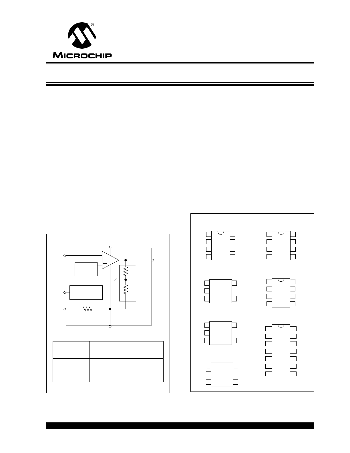
Block Diagram
Description
The Microchip Technology Inc. MCP6G01/1R/1U/2/3/4
are analog Selectable Gain Amplifiers (SGA). They can
be configured for gains of +1 V/V, +10 V/V, and
+50 V/V through the Gain Select input pin(s). The Chip
Select pin on the MCP6G03 can put it into shutdown to
conserve power. These SGAs are optimized for single
supply applications requiring reasonable quiescent
current and speed.
The single amplifiers MCP6G01, MCP6G01R,
MCP6G01U, and MCP6G03, are available in 5-pin
SOT-23 package and the dual amplifier MCP6G02, are
available in 8-pin SOIC and MSOP packages. The
quad amplifier MCP6G04 is available in 14-pin SOIC
and TSSOP packages. All parts are fully specified from
-40°C to +125°C.
Package Types
V
OUT
V
DD
GSEL
V
IN
V
SS
3
R
F
R
G
Gain Select
Logic
Gain
Switches
Resistor Lad
der
(R
LA
D
)
Gain
(V/V)
GSEL Voltage (Typ.)
(V)
1
V
DD
/2 (or open)
10
0
50
V
DD
Note:
V
SS
is assumed to be 0V
CS
(MCP6G03
only)
5 M
Ω
V
IN
GSEL
V
SS
V
OUT
V
DD
1
2
3
4
8
7
6
5
NC
NC
NC
GSEL
A
V
OUTA
V
INA
GSEL
C
V
INC
1
2
3
4
14
13
12
11 V
SS
V
OUTC
GSEL
D
5
6
7
10
9
8
V
DD
GSEL
B
V
OUTD
V
OUTB
V
IND
V
INB
MCP6G01
SOIC, MSOP
V
INA
GSEL
A
V
SS
GSEL
B
V
OUTB
1
2
3
4
8
7
6
5
V
DD
V
INB
V
OUTA
MCP6G02
SOIC, MSOP
MCP6G04
SOIC, TSSOP
V
IN
GSEL
V
SS
V
OUT
V
DD
1
2
3
4
8
7
6
5
CS
NC
NC
MCP6G03
SOIC, MSOP
V
DD
1
2
3
5
4
V
SS
V
OUT
V
IN
GSEL
MCP6G01R
SOT-23-5
V
SS
1
2
3
5
4
V
DD
V
IN
GSEL
V
OUT
MCP6G01U
SOT-23-5
V
SS
1
2
3
5
4
V
DD
V
OUT
V
IN
GSEL
MCP6G01
SOT-23-5
110 µA Selectable Gain Amplifier
MCP6G01/1R/1U/2/3/4
DS22004B-page 2
© 2006 Microchip Technology Inc.
1.0
ELECTRICAL
CHARACTERISTICS
Absolute Maximum Ratings †
V
DD
– V
SS
........................................................................7.0V
Current at Analog Input Pin (V
IN
)
......................................±2 mA
Analog Input (V
IN
) †† ..................... V
SS
– 1.0V to V
DD
+ 1.0V
All other Inputs and Outputs........... V
SS
– 0.3V to V
DD
+ 0.3V
Output Short Circuit Current...................................continuous
Current at Output and Supply Pins
................................ ±30 mA
Storage Temperature.....................................-65°C to +150°C
Junction Temperature..................................................+150°C
ESD protection on all pins (HBM; MM)
................ ≥ 4 kV; 200V
† Notice: Stresses above those listed under “Absolute
Maximum Ratings” may cause permanent damage to the
device. This is a stress rating only and functional operation of
the device at those or any other conditions above those
indicated in the operational listings of this specification is not
implied. Exposure to maximum rating conditions for extended
periods may affect device reliability.
†† See Section 4.1.4 “Input Voltage and Current Limits”.
DC ELECTRICAL CHARACTERISTICS
Electrical Specifications: Unless otherwise indicated, T
A
= +25°C, V
DD
= +1.8V to +5.5V, V
SS
= GND, G = +1 V/V,
V
IN
= (0.3V)/G, R
L
= 100 k
Ω to V
DD
/2, GSEL = V
DD
/2, and CS is tied low.
Parameters
Sym
Min
Typ
Max
Units
Conditions
Amplifier Inputs (V
IN
)
Input Offset Voltage
V
OS
–4.5
±1.0
+4.5
mV
G = +1
—
±1.0
—
mV
G = +10, +50
Input Offset Voltage Drift
ΔV
OS
/
ΔT
A
—
±2
—
µV/°C
G = +1, T
A
= -40°C to +125°C
Power Supply Rejection Ratio
PSRR
65
80
—
dB
G = +1 (Note 1)
Input Bias Current
I
B
—
1
—
pA
Input Bias Current at
I
B
—
30
—
pA
T
A
= +85°C
Temperature
I
B
—
1000
5000
pA
T
A
= +125°C
Input Impedance
Z
IN
—
10
13
||6
—
Ω||pF
Amplifier Gain
Nominal Gains
G
—
1 to 50
—
V/V
+1, +10 or +50
DC Gain Error G = +1
g
E
–0.3
—
+0.3
%
V
OUT
≈ 0.3V to V
DD
− 0.3V
G
≥ +10
g
E
–1.0
—
+1.0
%
V
OUT
≈ 0.3V to V
DD
− 0.3V
DC Gain Drift G = +1
ΔG/ΔT
A
—
±1
—
ppm/°C
T
A
= -40°C to +125°C
G
≥ +10
ΔG/ΔT
A
—
±4
—
ppm/°C
T
A
= -40°C to +125°C
Ladder Resistance (Note 1)
Ladder Resistance
R
LAD
200
350
500
k
Ω
Ladder Resistance
across Temperature
ΔR
LAD
/
ΔT
A
—
–1800
—
ppm/°C
T
A
= -40°C to +125°C
Amplifier Output
DC Output Non-linearity G = +1
V
ONL
–0.2
—
+0.2
% of FSR V
OUT
= 0.3V to V
DD
– 0.3V,
V
DD
= 1.8V
V
ONL
–0.1
—
+0.1
% of FSR V
OUT
= 0.3V to V
DD
– 0.3V,
V
DD
= 5.5V
DC Output Non-linearity, G = +10, +50
V
ONL
–0.05
—
+0.05
% of FSR V
OUT
= 0.3V to V
DD
– 0.3V
Maximum Output Voltage Swing
V
OH
, V
OL
V
SS
+10
—
V
DD
–10
mV
G = +1; 0.3V output overdrive
V
OH
, V
OL
V
SS
+10
—
V
DD
–10
mV
G
≥ +10; 0.5V output overdrive
Short Circuit Current
I
SC
—
±7
—
mA
V
DD
= 1.8V
I
SC
—
±20
—
mA
V
DD
= 5.5V
Note 1:
R
LAD
(R
F
+R
G
in
Figure 4-1
) connects V
SS
, V
OUT
, and the inverting input of the internal amplifier. Thus, V
SS
is coupled
to the internal amplifier and the PSRR spec describes PSRR+ only. It is recommended that the V
SS
pin be tied directly
to ground to avoid noise problems.
2:
I
Q
includes current in R
LAD
(typically 0.6 µA at V
OUT
= 0.3V), and excludes digital switching currents.
© 2006 Microchip Technology Inc.
DS22004B-page 3
MCP6G01/1R/1U/2/3/4
Power Supply
Supply Voltage
V
DD
1.8
—
5.5
V
Quiescent Current per Amplifier
I
Q
60
110
170
µA
I
O
= 0 (Note 2)
DC ELECTRICAL CHARACTERISTICS (CONTINUED)
Electrical Specifications: Unless otherwise indicated, T
A
= +25°C, V
DD
= +1.8V to +5.5V, V
SS
= GND, G = +1 V/V,
V
IN
= (0.3V)/G, R
L
= 100 k
Ω to V
DD
/2, GSEL = V
DD
/2, and CS is tied low.
Parameters
Sym
Min
Typ
Max
Units
Conditions
Note 1:
R
LAD
(R
F
+R
G
in
Figure 4-1
) connects V
SS
, V
OUT
, and the inverting input of the internal amplifier. Thus, V
SS
is coupled
to the internal amplifier and the PSRR spec describes PSRR+ only. It is recommended that the V
SS
pin be tied directly
to ground to avoid noise problems.
2:
I
Q
includes current in R
LAD
(typically 0.6 µA at V
OUT
= 0.3V), and excludes digital switching currents.
AC ELECTRICAL CHARACTERISTICS
Electrical Specifications: Unless otherwise indicated, T
A
= +25°C, V
DD
= +1.8V to +5.5V, V
SS
= GND, G = +1 V/V,
V
IN
= (0.3V)/G, R
L
= 100 k
Ω to V
DD
/2, C
L
= 60 pF, GSEL = V
DD
/2, and CS is tied low.
Parameters
Sym
Min
Typ
Max
Units
Conditions
Frequency Response
-3dB Bandwidth
BW
—
900
—
kHz
G = +1, V
OUT
< 100 mV
P-P
(Note 1)
BW
—
350
—
kHz
G = +10, V
OUT
< 100 mV
P-P
(Note 1)
BW
—
250
—
kHz
G = +50, V
OUT
< 100 mV
P-P
(Note 1)
Gain Peaking
GPK
—
0.3
—
dB
G = +1; V
OUT
< 100 mV
P-P
GPK
—
0
—
dB
G = +10, V
OUT
< 100 mV
P-P
GPK
—
0.7
—
dB
G = +50; V
OUT
< 100 mV
P-P
Total Harmonic Distortion plus Noise
f = 1 kHz, G = +1 V/V
THD+N
—
0.0029
—
%
V
OUT
= 1.75V ± 1.4V
PK
, V
DD
= 5.0V,
BW = 80 kHz
f = 1 kHz, G = +10 V/V
THD+N
—
0.18
—
%
V
OUT
= 2.5V ± 1.4V
PK
, V
DD
= 5.0V,
BW = 80 kHz
f = 1 kHz, G = +50 V/V
THD+N
—
1.3
—
%
V
OUT
= 2.5V ± 1.4V
PK
, V
DD
= 5.0V,
BW = 80 kHz
Step Response
Slew Rate
SR
—
0.50
—
V/µs
G = 1
SR
—
2.3
—
V/µs
G = 10
SR
—
4.5
—
V/µs
G = 50
Noise
Input Noise Voltage
E
ni
—
9
—
µV
P-P
f = 0.1 Hz to 10 Hz (Note 2)
E
ni
—
50
—
µV
P-P
f = 0.1 Hz to 30 kHz (Note 2)
Input Noise Voltage Density
e
ni
—
38
—
nV/
√Hz G = +1 V/V, f = 10 kHz (Note 2)
e
ni
—
46
—
nV/
√Hz G = +10 V/V, f = 10 kHz (Note 2)
e
ni
—
41
—
nV/
√Hz G = +50 V/V, f = 10 kHz (Note 2)
Input Noise Current Density
i
ni
—
4
—
fA/
√Hz f = 10 kHz
Note 1:
See
Table 4-1
for a list of typical numbers and
Figure 2-31
for the frequency response versus gain.
2:
E
ni
and e
ni
include ladder resistance thermal noise.
MCP6G01/1R/1U/2/3/4
DS22004B-page 4
© 2006 Microchip Technology Inc.
DIGITAL ELECTRICAL CHARACTERISTICS
Electrical Specifications: Unless otherwise indicated, T
A
= 25°C, V
DD
= +1.8V to +5.5V, V
SS
= GND, G = +1 V/V, V
IN
= (0.3V)/G,
R
L
= 100 k
Ω to V
DD
/2, C
L
= 60 pF, GSEL = V
DD
/2, and CS is tied low.
Parameters
Sym
Min
Typ
Max
Units
Conditions
CS Low Specifications
CS Logic Threshold, Low
V
CSL
0
—
0.2V
DD
V
CS = 0V
CS Input Current, Low
I
CSL
—
30
—
pA
CS = 0V
CS High Specifications
CS Logic Threshold, High
V
CSH
0.8V
DD
—
V
DD
V
CS = V
DD
CS Input Current, High
I
CSH
—
0.8
—
µA
CS = V
DD
= 5.5V
Quiescent Current per Amplifier,
Shutdown Mode (I
DD
)
I
DD_SHDN
—
120
—
pA
CS = V
DD
, MCP6G03
Quiescent Current per Amplifier,
Shutdown Mode (I
SS
) (Note 3)
I
SS_SHDN
—
–2.4
—
µA
CS = V
DD
= 1.8V, MCP6G03
I
SS_SHDN
—
–7.2
—
µA
CS = V
DD
= 5.5V, MCP6G03
CS Dynamic Specifications
Input Capacitance
C
CS
—
10
—
pF
Input Rise/Fall Times
t
CSRF
—
—
2
µs
(Note 2)
CS Low to Amplifier Output High
Turn-on Time
t
CSON
—
40
—
µs
G = +1 V/V, V
DD
= 1.8V, V
IN
= 0.9V
DD
CS = 0.2V
DD
to V
OUT
= 0.8V
DD
t
CSON
—
7
—
µs
G = +1 V/V, V
DD
= 5.5V, V
IN
= 0.9V
DD
CS = 0.2V
DD
to V
OUT
= 0.8V
DD
CS High to Amplifier Output High-Z
Turn-off Time
t
CSOFF
—
30
—
µs
G = +1 V/V, V
IN
= V
DD
/2,
CS = 0.8V
DD
to V
OUT
= 0.1V
DD
/2
Hysteresis
V
CSHY
—
0.40
—
V
V
DD
= 1.8V
V
CSHY
—
0.55
—
V
V
DD
= 5.5V
GSEL Specifications (Note 1)
GSEL Logic Threshold, Low
V
GSL
0.15V
DD
—
0.35V
DD
V
Gain changes between 1 and 10,
I
GSEL
= 0
GSEL Logic Threshold, High
V
GSH
0.65V
DD
—
0.85V
DD
V
Gain changes between 1 and 50,
I
GSEL
= 0
GSEL Input Current, Low
I
GSL
–10
—
–1.5
µA
GSEL voltage = 0.3V
DD
GSEL Input Current, High
I
GSH
+1.5
—
+10
µA
GSEL voltage = 0.7V
DD
GSEL Dynamic Specifications (Note 1)
Input Capacitance
C
GSEL
—
8
—
pF
Input Rise/Fall Times
t
GSRF
—
—
10
µs
(Note 2)
Hysteresis
V
GSHY
—
45
—
mV
V
DD
= 1.8V
V
GSHY
—
95
—
mV
V
DD
= 5.5V
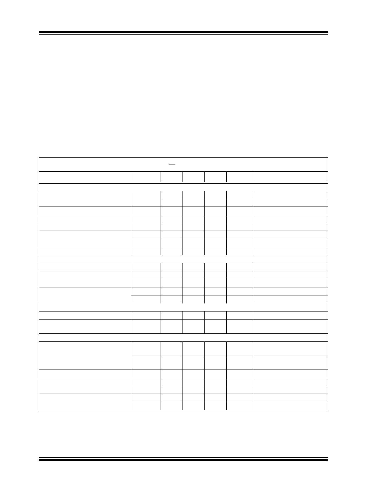
GSEL Low to Valid Output Time,
G = +1 to +10 Select
t
GSL1
—
10
—
µs
V
IN
= 150 mV,
GSEL = 0.25V
DD
to V
OUT
= 1.37V
GSEL Middle to Valid Output Time,
G = +10 to +1 Select
t
GSM10
—
12
—
µs
V
IN
= 150 mV,
GSEL = 0.25V
DD
to V
OUT
= 0.28V
GSEL High to Valid Output Time,
G = +1 to +50 Select
t
GSH1
—
9
—
µs
V
IN
= 30 mV,
GSEL = 0.75V
DD
to V
OUT
= 1.35V
GSEL Middle to Valid Output Time,
G = +50 to +1 Select
t
GSM50
—
8
—
µs
V
IN
= 30 mV,
GSEL = 0.75V
DD
to V
OUT
= 0.18V
Note 1:
GSEL is a tri-level input pin. The gain is 10 when its voltage is low, 1 when it is at mid-suppy, and 50 when it is high.
2:
Not tested in production. Set by design and characterization.
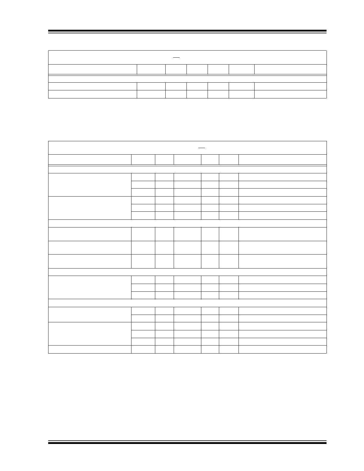
3:
I
SS_SHDN
includes the current through the CS pin, R
L
and R
LAD
, and excludes digital switching currents. The block dia-
gram on the from page shows these current paths (through V
SS
).
© 2006 Microchip Technology Inc.
DS22004B-page 5
MCP6G01/1R/1U/2/3/4
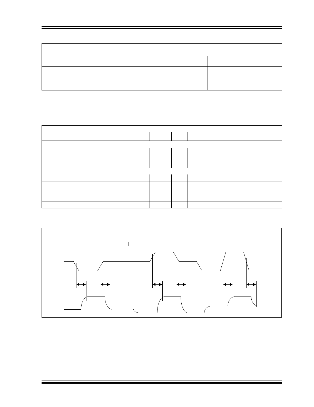
FIGURE 1-1:
Gain Select Timing Diagram.
GSEL High to Valid Output Time,
G = +10 to +50 Select
t
GSH10
—
12
—
µs
V
IN
= 30 mV,
GSEL = 0.75V
DD
to V
OUT
= 1.38V
GSEL Low to Valid Output Time,
G = +50 to +10 Select
t
GSL50
—
9
—
µs
V
IN
= 30 mV,
GSEL = 0.25V
DD
to V
OUT
= 0.42V
DIGITAL ELECTRICAL CHARACTERISTICS (CONTINUED)
Electrical Specifications: Unless otherwise indicated, T
A
= 25°C, V
DD
= +1.8V to +5.5V, V
SS
= GND, G = +1 V/V, V
IN
= (0.3V)/G,
R
L
= 100 k
Ω to V
DD
/2, C
L
= 60 pF, GSEL = V
DD
/2, and CS is tied low.
Parameters
Sym
Min
Typ
Max
Units
Conditions
Note 1:
GSEL is a tri-level input pin. The gain is 10 when its voltage is low, 1 when it is at mid-suppy, and 50 when it is high.
2:
Not tested in production. Set by design and characterization.
3:
I
SS_SHDN
includes the current through the CS pin, R
L
and R
LAD
, and excludes digital switching currents. The block dia-
gram on the from page shows these current paths (through V
SS
).
TEMPERATURE CHARACTERISTICS
Electrical Specifications: Unless otherwise indicated, V
DD
= +1.8V to +5.5V, and V
SS
= GND.
Parameters
Sym
Min
Typ
Max
Units
Conditions
Temperature Ranges
Specified Temperature Range
T
A
–40
—
+125
°C
Operating Temperature Range
T
A
–40
—
+125
°C
(Note 1)
Storage Temperature Range
T
A
–65
—
+150
°C
Thermal Package Resistances
Thermal Resistance, 5L-SOT-23
θ
JA
—
256
—
°C/W
Thermal Resistance, 8L-SOIC
θ
JA
—
163
—
°C/W
Thermal Resistance, 8L-MSOP
θ
JA
—
206
—
°C/W
Thermal Resistance, 14L-SOIC
θ
JA
—
120
—
°C/W
Thermal Resistance, 14L-TSSOP
θ
JA
—
100
—
°C/W
Note 1:
The MCP6G01/1R/1U/2/3/4 family of SGAs operates over this temperature range, but operation must not cause T
J
to
exceed Maximum Junction Temperature (+150°C).
GSEL
V
OUT
t
GSL1
0.15V
1.50V
V
IN
0.150V
0.030V
0.15V
t
GSM10
0.03V
1.50V
t
GSH1
0.03V
t
GSM50
0.30V
1.50V
t
GSH10
0.30V
t
GSL50
MCP6G01/1R/1U/2/3/4
DS22004B-page 6
© 2006 Microchip Technology Inc.
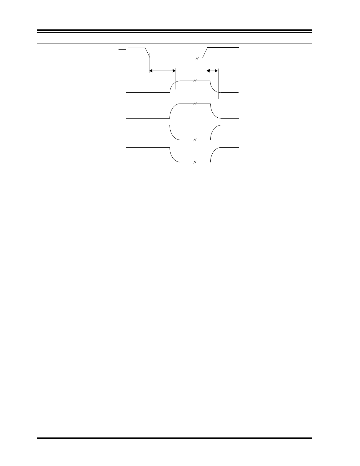
FIGURE 1-2:
SGA Chip Select Timing Diagram.
CS
t
CSOFF
V
OUT
t
CSON
High-Z
High-Z
I
DD
120 pA (typ.)
110 µA (typ.)
0.9V
DD
I
SS
–V
DD
/ 7 M
Ω (typ.)
–110 µA (typ.)
I
CS
30 pA (typ.)
V
DD
/ 7 M
Ω (typ.)
© 2006 Microchip Technology Inc.
DS22004B-page 7
MCP6G01/1R/1U/2/3/4
1.1
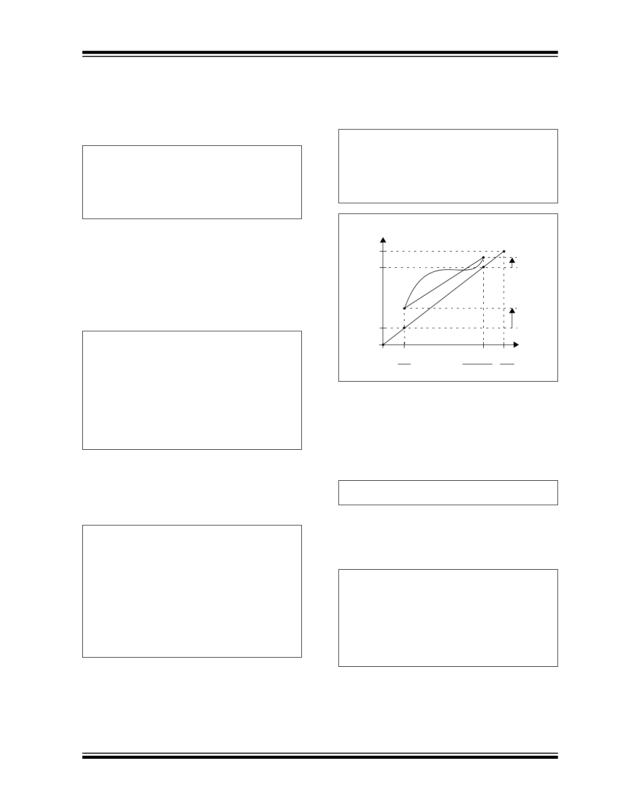
DC Output Voltage Specs / Model
1.1.1
IDEAL MODEL
The ideal SGA output voltage (V
OUT
) is (see
Figure 1-3
):
EQUATION 1-1:
This equation holds when there are no gain or offset
errors.
1.1.2
LINEAR MODEL
The SGA’s linear region of operation is modeled by the
line V
O_LIN
shown in
Figure 1-3
. V
O_LIN
includes offset
and gain errors, but does not include non-linear effects.
EQUATION 1-2:
This line’s endpoints are 0.3V from the supply rails
(V
O_ID
= 0.3V and V
DD
– 0.3V). The gain error and
input offset voltage specifications (in the electrical
specifications) relate to
Figure 1-3
as follows:
EQUATION 1-3:
The input offset specification describes V
OS
at
G = +1 V/V.
The DC Gain Drift (
ΔG/ΔT
A
) can be calculated from the
change in g
E
across temperature. This is shown in the
following equation:
EQUATION 1-4:
FIGURE 1-3:
Output Voltage Model.
1.1.3
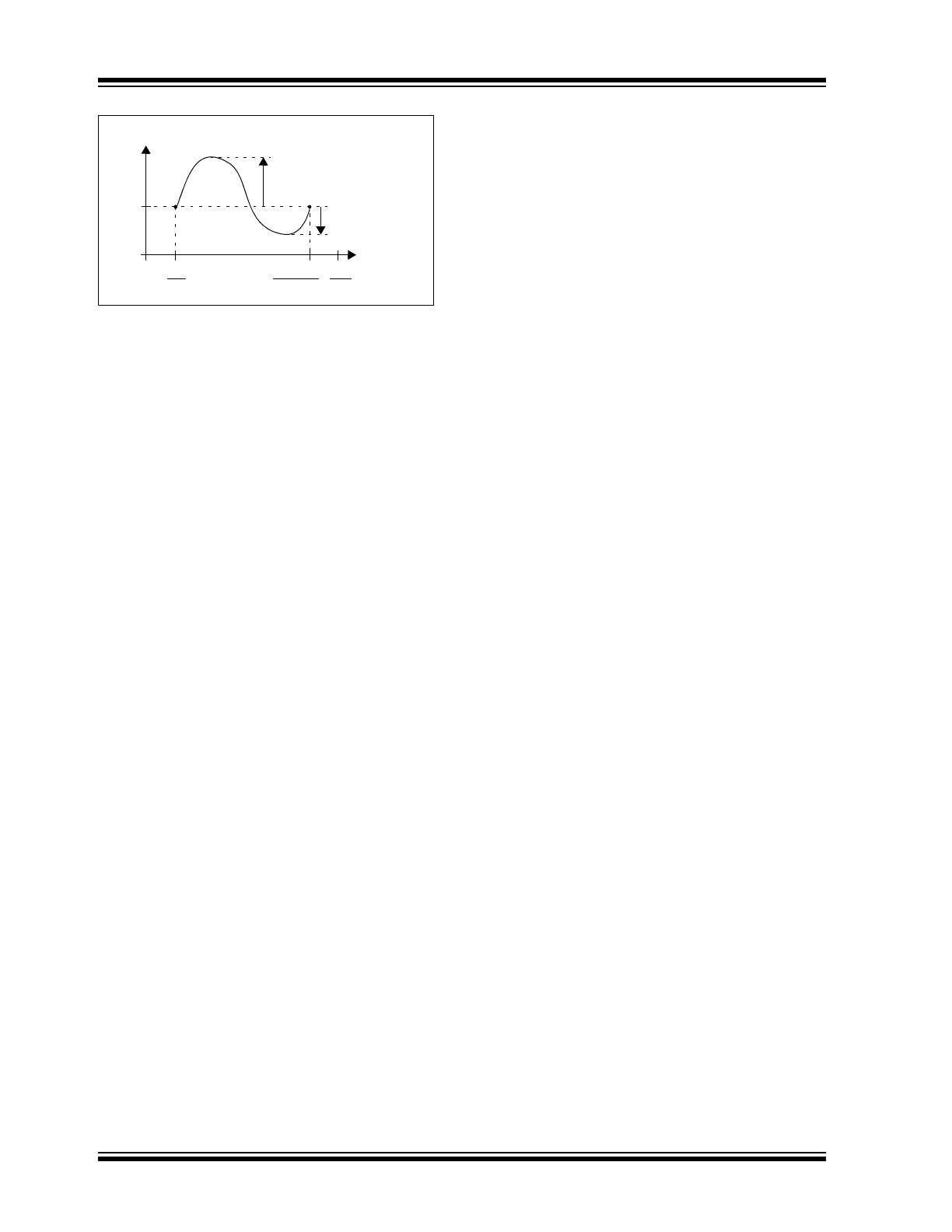
OUTPUT NON-LINEARITY
Figure 1-4
shows the Integral Non-Linearity (INL) of the
output voltage. INL is the output non-linearity error not
explained by V
O_LIN
:
EQUATION 1-5:
The output non-linearity specification (in the Electrical
Specifications, with units of % of FSR) is related to
Figure 1-4
by:
EQUATION 1-6:
Note that the Full Scale Range (FSR) is V
DD
– 0.6V
(0.3V to V
DD
– 0.3V).
Where:
G is the nominal gain
V
O_ID
GV
IN
=
V
REF
V
SS
0V
=
=
V
O_LIN
G 1 g
E
+
(
) V
IN
0.3V
G
------------ V
OS
+
–
⎝
⎠
⎛
⎞ 0.3V
+
=
V
REF
V
SS
0V
=
=
Where:
G is the nominal gain
g
E
is the gain error
V
OS
is the input offset voltage
g
E
100%
V
2
V
1
–
V
DD
0.6V
–
-----------------------------
⋅
=
V
OS
V
1
G 1 g
E
+
(
)
-------------------------,
=
G
+1
=
Where:
V
1
V
OUT
V
O_ID
,
–
=
V
O_ID
0.3V
=
V
2
V
OUT
V
O_ID
,
–
=
V
O_ID
V
DD
0.3V
–
=
G
Δ
T
A
Δ
⁄
G
g
E
Δ
T
A
Δ
----------,
⋅
=
in units of V/V/°C
G
Δ
T
A
Δ
⁄
100%
g
E
Δ
T
A
Δ
----------,
⋅
=
in units of %/°C
0
0
0.3
V
DD
-0.3
V
DD
V
OUT
V
OUT
(V)
V
IN
(V)
0.3
V
DD
-0.3 V
DD
G
G
G
V
1
V
O_
ID
V
O_
LIN
V
2
INL
V
OUT
V
O_LIN
–
=
V
ONL
100%
max V
3
V
4
,
(
)
V
DD
0.6V
–
-------------------------------
⋅
=
V
3
max INL
–
(
)
=
Where:
V
4
max INL
(
)
=
MCP6G01/1R/1U/2/3/4
DS22004B-page 8
© 2006 Microchip Technology Inc.
FIGURE 1-4:
Output Voltage INL.
0
INL (V)
V
IN
(V)
0.3
V
DD
-0.3 V
DD
G
G
G
0
V
3
V
4
© 2006 Microchip Technology Inc.
DS22004B-page 9
MCP6G01/1R/1U/2/3/4
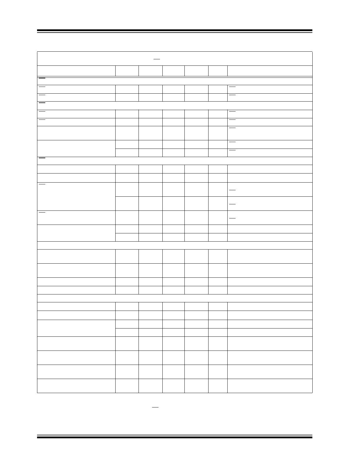
2.0
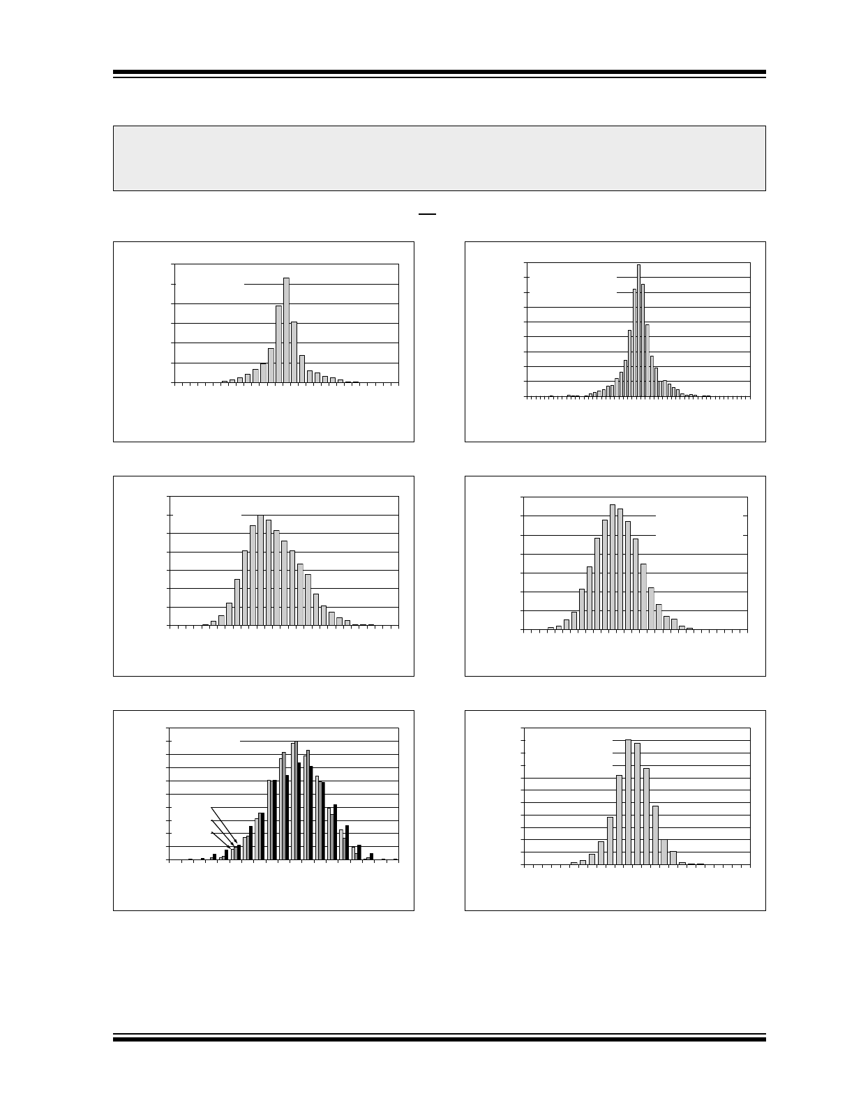
TYPICAL PERFORMANCE CURVES
Note: Unless otherwise indicated, T
A
= +25°C, V
DD
= +1.8V to +5.5V, V
SS
= GND, G = +1 V/V, V
IN
= (0.3V)/G,
R
L
= 100 k
Ω to V
DD
/2, C
L
= 60 pF, GSEL = V
DD
/2, and CS is tied low.
FIGURE 2-1:
DC Gain Error, G = +1.
FIGURE 2-2:
DC Gain Error, G
≥ +10.
FIGURE 2-3:
Input Offset Voltage.
FIGURE 2-4:
DC Gain Drift, G = +1.
FIGURE 2-5:
DC Gain Drift, G
≥ +10.
FIGURE 2-6:
Input Offset Voltage Drift.
Note:
The graphs and tables provided following this note are a statistical summary based on a limited number of
samples and are provided for informational purposes only. The performance characteristics listed herein
are not tested or guaranteed. In some graphs or tables, the data presented may be outside the specified
operating range (e.g., outside specified power supply range) and therefore outside the warranted range.
0%
5%
10%
15%
20%
25%
30%
-0
.2
8
-0
.2
4
-0
.2
0
-0
.1
6
-0
.1
2
-0
.0
8
-0
.0
4
0.0
0
0.0
4
0.0
8
0.1
2
0.1
6
0.2
0
0.2
4
0.2
8
DC Gain Error (%)
Per
cen
ta
g
e of
Occ
u
rr
en
ces
2460 Samples
G = +1
0%
2%
4%
6%
8%
10%
12%
14%
-0
.7
-0
.6
-0
.5
-0
.4
-0
.3
-0
.2
-0
.1
0.
0
0.
1
0.
2
0.
3
0.
4
0.
5
0.
6
0.
7
DC Gain Error (%)
Per
cen
ta
g
e of
Occ
u
rr
en
ces
4916 Samples
G ≥ +10
0%
2%
4%
6%
8%
10%
12%
14%
16%
18%
20%
-4
.5
-3
.5
-2
.5
-1
.5
-0
.5
0.
5
1.
5
2.
5
3.
5
4.
5
Input Offset Voltage (mV)
P
erce
n
ta
ge
o
f O
ccu
rr
en
ces
2460 Samples
G = +50
G = +10
G = +1
0%
2%
4%
6%
8%
10%
12%
14%
16%
18%
-5
-4
-3
-2
-1
0
1
2
3
4
5
DC Gain Drift (ppm/°C)
Perce
n
ta
g
e
of Oc
curre
n
c
es
2459 Samples
G = +1
T
A
= -40 to +125°C
0%
2%
4%
6%
8%
10%
12%
14%
-1
4
-1
2
-1
0
-8
-6
-4
-2
0
2
4
6
8
10
12
14
DC Gain Drift (ppm/°C)
Perce
n
ta
g
e
of Oc
curre
n
c
es
4912 Samples
G ≥ +10
T
A
= -40 to +125°C
0%
2%
4%
6%
8%
10%
12%
14%
16%
18%
20%
22%
-1
2
-1
0
-8
-6
-4
-2
0
2
4
6
8
10
12
Input Offset Voltage Drift (µV/°C)
Per
cen
ta
g
e of
Oc
cu
rren
ce
s
1612 Samples
G = +1, +10, +50
T
A
= -40 to +125°C
MCP6G01/1R/1U/2/3/4
DS22004B-page 10
© 2006 Microchip Technology Inc.
Note: Unless otherwise indicated, T
A
= +25°C, V
DD
= +1.8V to +5.5V, V
SS
= GND, G = +1 V/V, V
IN
= (0.3V)/G,
R
L
= 100 k
Ω to V
DD
/2, C
L
= 60 pF, GSEL = V
DD
/2, and CS is tied low.
FIGURE 2-7:
The MCP6G01/1R/1U/2/3/4
family shows no phase reversal under overdrive.
FIGURE 2-8:
PSRR vs. Temperature.
FIGURE 2-9:
Input Noise Voltage Density
vs. Frequency.
FIGURE 2-10:
Crosstalk vs. Frequency,
with G = 50 (circuit in
Figure 4-7
).
FIGURE 2-11:
PSRR vs. Frequency.
FIGURE 2-12:
Quiescent Current vs.
Supply Voltage.
-1
0
1
2
3
4
5
6
0.0E+00
1.0E-03
2.0E-03
3.0E-03
4.0E-03
5.0E-03
6.0E-03
7.0E-03
8.0E-03
9.0E-03
1.0E-02
Time (1 ms/div)
Inpu
t,
O
u
tput
Volta
g
e (V)
V
DD
= 5.0V
G = +1 V/V
V
IN
V
OUT
70
80
90
100
110
120
-50
-25
0
25
50
75
100
125
Ambient Temperature (°C)
PSRR
(
d
B)
10
100
1000
10000
0.1
1
10
100
1000 10000 10000
0
Frequency (Hz)
Input Noise Voltage Density
(nV/
Hz)
1k
10k
100k
1
10
100
0.1
G = +1
= +10
= +50
-120
-110
-100
-90
-80
-70
-60
-50
-40
-30
-20
-10
0
1.E+03
1.E+04
1.E+05
Frequency (Hz)
C
ros
sta
lk, Inpu
t R
eferre
d
(d
B)
1k
100k
10k
V
DD
= 5.0V
G = 50 V/V
R
S
= 0 Ω
R
S
= 1 MΩ
R
S
= 100 kΩ
R
S
= 10 kΩ
20
30
40
50
60
70
80
90
100
1000
10000
100000
Frequency (Hz)
Po
w
er Sup
p
ly
Reje
ct
ion
Rat
io
(dB
)
Input Referred
G = 1
G = 10
G = 50
V
DD
= 1.8V
V
DD
= 5.5V
100
1k
10k
100k
0
20
40
60
80
100
120
140
160
0.0 0.5 1.0 1.5 2.0 2.5 3.0 3.5 4.0 4.5 5.0 5.5
Power Supply Voltage (V)
Qu
ie
scen
t C
u
rren
t (
m
A
)
T
A
= +25°C
T
A
= –40°C
T
A
= +125°C
T
A
= +85°C