

2016 Microchip Technology Inc.
DS00002297A-page 1
Features
• Single-Chip 10BASE-T/100BASE-TX IEEE 802.3
Compliant Ethernet Transceiver
• MII Interface Support
• Back-to-Back Mode Support for a 100 Mbps Cop-
per Repeater
• MDC/MDIO Management Interface for PHY Reg-
ister Configuration
• Programmable Interrupt Output
• LED Outputs for Link, Activity, and Speed Status
Indication
• On-Chip Termination Resistors for the Differential
Pairs
• Baseline Wander Correction
• HP Auto MDI/MDI-X to Reliably Detect and Cor-
rect Straight-Through and Crossover Cable Con-
nections with Disable and Enable Option
• Auto-Negotiation to Automatically Select the
Highest Link-Up Speed (10/100 Mbps) and
Duplex (Half/Full)
• Energy Efficient Ethernet (EEE) Support with
Low-Power Idle (LPI) Mode and Clock Stoppage
for 100BASE-TX and Transmit Amplitude Reduc-
tion with 10BASE-Te Option
• Wake-on-LAN (WOL) Support with Either Magic
Packet, Link Status Change, or Robust Custom-
Packet Detection
• LinkMD
®
TDR-Based Cable Diagnostics to Iden-
tify Faulty Copper Cabling
• HBM ESD Rating (6 kV)
• Parametric NAND Tree Support for Fault Detec-
tion Between Chip I/Os and the Board
• Loopback Modes for Diagnostics
• Power-Down and Power-Saving Modes
• Single 3.3V Power Supply with V
DD
I/O Options
for 1.8V, 2.5V, or 3.3V
• Built-In 1.2V Regulator for Core
• Available in 48-Pin 7 mm x 7 mm LQFP Package
Target Applications
• Game Consoles
• IP Phones
• IP Set-Top Boxes
• IP TVs
• LOM
• Printers
KSZ8091MLX
10BASE-T/100BASE-TX
Physical Layer Transceiver

KSZ8091MLX
DS00002297A-page 2
2016 Microchip Technology Inc.
TO OUR VALUED CUSTOMERS
It is our intention to provide our valued customers with the best documentation possible to ensure successful use of your Microchip
products. To this end, we will continue to improve our publications to better suit your needs. Our publications will be refined and
enhanced as new volumes and updates are introduced.
If you have any questions or comments regarding this publication, please contact the Marketing Communications Department via
E-mail at
docerrors@microchip.com
. We welcome your feedback.
Most Current Data Sheet
To obtain the most up-to-date version of this data sheet, please register at our Worldwide Web site at:
http://www.microchip.com
You can determine the version of a data sheet by examining its literature number found on the bottom outside corner of any page.
The last character of the literature number is the version number, (e.g., DS30000000A is version A of document DS30000000).
Errata
An errata sheet, describing minor operational differences from the data sheet and recommended workarounds, may exist for cur-
rent devices. As device/documentation issues become known to us, we will publish an errata sheet. The errata will specify the
revision of silicon and revision of document to which it applies.
To determine if an errata sheet exists for a particular device, please check with one of the following:
• Microchip’s Worldwide Web site;
http://www.microchip.com
• Your local Microchip sales office (see last page)
When contacting a sales office, please specify which device, revision of silicon and data sheet (include -literature number) you are
using.
Customer Notification System
Register on our web site at
www.microchip.com
to receive the most current information on all of our products.

2016 Microchip Technology Inc.
DS00002297A-page 3
KSZ8091MLX
Table of Contents
1.0 Introduction ..................................................................................................................................................................................... 4
2.0 Pin Description and Configuration .................................................................................................................................................. 5
3.0 Functional Description .................................................................................................................................................................. 12
4.0 Register Descriptions .................................................................................................................................................................... 32
5.0 Operational Characteristics ........................................................................................................................................................... 49
6.0 Electrical Characteristics ............................................................................................................................................................... 50
7.0 Timing Diagrams ........................................................................................................................................................................... 52
8.0 Reset Circuit ................................................................................................................................................................................. 60
9.0 Reference Circuits — LED Strap-In Pins ...................................................................................................................................... 61
10.0 Reference Clock - Connection and Selection ............................................................................................................................. 62
11.0 Magnetic - Connection and Selection ......................................................................................................................................... 63
12.0 Package Outline .......................................................................................................................................................................... 65
Appendix A: Data Sheet Revision History ........................................................................................................................................... 66
The Microchip Web Site ...................................................................................................................................................................... 67
Customer Change Notification Service ............................................................................................................................................... 67
Customer Support ............................................................................................................................................................................... 67
Product Identification System ............................................................................................................................................................. 68
KSZ8091MLX
DS00002297A-page 4
2016 Microchip Technology Inc.
1.0
INTRODUCTION
1.1
General Description
The KSZ8091MLX is a single-supply 10BASE-T/100BASE-TX Ethernet physical layer transceiver for transmission and
reception of data over standard CAT-5 unshielded twisted pair (UTP) cable.
The KSZ8091MLX is a highly-integrated, compact solution. It reduces board cost and simplifies board layout by using
on-chip termination resistors for the differential pairs, by integrating a low-noise regulator to supply the 1.2V core, and
by offering a flexible 1.8/2.5/3.3V digital I/O interface.
The KSZ8091MLX offers the Media Independent Interface (MII) for direct connection with MII-compliant Ethernet MAC
processors and switches.
Energy Efficient Ethernet (EEE) provides further power saving during idle traffic periods and Wake-on-LAN (WOL) pro-
vides a mechanism for the KSZ8091MLX to wake up a system that is in standby power mode.
The KSZ8091MLX is available in the 48-pin, lead-free LQFP package.
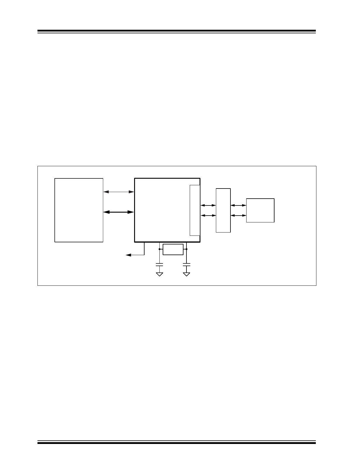
FIGURE 1-1:
SYSTEM BLOCK DIAGRAM
KSZ8091MLX
MAGNETICS
RJ-45
CONNECTOR
MEDIA TYPES:
10BASE-T
100BASE-TX
ON-CHIP TERMINATION
RESISTORS
MII
MDC/ MDIO
MANAGEMENT
XO
XI
25MHz
XTAL
22pF
22pF
10/100Mbps
MII MAC
PME_N
(SYSTEM
POWER
CIRCUIT)
2016 Microchip Technology Inc.
DS00002297A-page 5
KSZ8091MLX
2.0
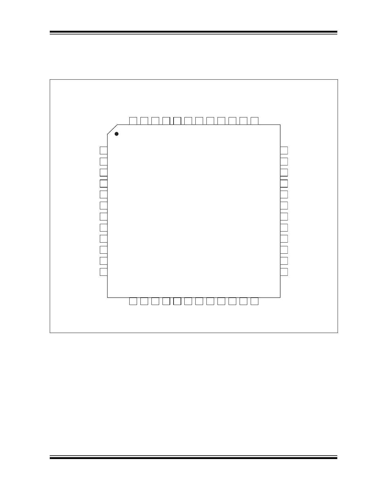
PIN DESCRIPTION AND CONFIGURATION
FIGURE 2-1:
48-PIN 7 MM X 7 MM LQFP ASSIGNMENT (TOP VIEW)
1
NC
NC
TXC /
PME_EN
RST
#
REXT
GND
RXER /
ISO
GND
VDD_1.2
GND
GND
GND
GND
XO
NC
NC
TXD1
TXD0
TXEN
LED
1
/
SPEED
LED0 / PME_N1 /
NWAYEN
CRS
/
CONFIG
1
TXER
2
3
8
13
14
16
17
29
30
31
32
33
34
35
36
41
42
43
44
45
46
47
48
RXP
TXM
RXM
9
10
11
GND
24
TXD
3
TXD
2
GND
COL
/
CONFIG
0
37
38
39
40
RXC /
B-CAST_OFF
VDDIO
NC
RXDV /
CONFIG2
25
26
27
28
RXD
2 /
PHYAD
1
RXD
1 /
PHYAD
2
RXD
0 /
DUPLEX
21
22
23
MDIO
MDC
RXD
3
/
PHYAD
0
18
19
20
XI
15
TXP
12
VDD_1.2
NC
4
5
NC
VDDA_3.3
6
7
KSZ8091MLX
INTRP / PME_N2 /
NAND_TREE#

KSZ8091MLX
DS00002297A-page 6
2016 Microchip Technology Inc.
TABLE 2-1:
SIGNALS - KSZ8091MLX
Pin
Number
Pin
Name
Type
Note
2-1
Description
1
GND
GND
Ground.
2
GND
GND
Ground.
3
GND
GND
Ground.
4
VDD_1.2
P
1.2V core V
DD
. (Power supplied by KSZ8091MLX.)
Decouple with 2.2 µF and 0.1 µF capacitors to ground, and join with Pin 31 by
power trace or plane.
5
NC
—
No Connect. This pin is not bonded and can be left floating.
6
NC
—
No Connect. This pin is not bonded and can be left floating.
7
VDDA_3.3
P
3.3V analog V
DD
.
8
NC
—
No Connect. This pin is not bonded and can be left floating.
9
RXM
I/O
Physical Receive or Transmit Signal (– differential).
10
RXP
I/O
Physical Receive or Transmit Signal (+ differential).
11
TXM
I/O
Physical Transmit or Receive Signal (– differential).
12
TXP
I/O
Physical Transmit or Receive Signal (+ differential).
13
GND
GND
Ground.
14
XO
O
Crystal Feedback for 25 MHz crystal. This pin is a no connect if an oscillator
or external clock source is used.
15
XI
I
Crystal/Oscillator/External Clock Input (25 MHz ±50 ppm).
16
REXT
I
Set PHY Transmit Output Current. Connect a 6.49 kΩ resistor to ground on
this pin.
17
GND
GND
Ground.
18
MDIO
Ipu/
Opu
Management Interface (MII) Data I/O. This pin has a weak pull-up, is open-
drain, and requires an external 1.0 kΩ pull-up resistor.
19
MDC
Ipu
Management Interface (MII) Clock Input. This clock pin is synchronous to the
MDIO data pin.
20
RXD3/
PHYAD0
Ipu/O
MII mode: MII Receive Data Output[3] (
Note 2-2
).
Config mode: The pull-up/pull-down value is latched as PHYADDR[0] at the
de-assertion of reset. See the
Strap-In Options
section for details.
21
RXD2/
PHYAD1
Ipd/O
MII Mode: MII Receive Data Output[2] (
Note 2-2
).
Config. Mode: The pull-up/pull-down value is latched as PHYADDR[1] at the
de-assertion of reset. See the
Strap-In Options
section for details.
22
RXD1/
PHYAD2
Ipd/O
MII Mode: MII Receive Data Output[1] (
Note 2-2
).
Config. Mode: The pull-up/pull-down value is latched as PHYADDR[2] at the
de-assertion of reset. See the
Strap-In Options
section for details.
23
RXD0/
DUPLEX
Ipu/O
MII mode: MII Receive Data Output[0] (
Note 2-2
).
Config. Mode: The pull-up/pull-down value is latched as DUPLEX at the de-
assertion of reset. See the
Strap-In Options
section for details.

2016 Microchip Technology Inc.
DS00002297A-page 7
KSZ8091MLX
24
GND
GND
Ground.
25
VDDIO
P
3.3V, 2.5V, or 1.8V digital V
DD
.
26
NC
—
No Connect. This pin is not bonded and can be left floating.
27
RXDV/
CONFIG2
Ipd/O
MII Mode: MII Receive Data Valid Output
Config. Mode: The pull-up/pull-down value is latched as CONFIG2 at the de-
assertion of reset. See the
Strap-In Options
section for details.
28
RXC/
B-CAST_OFF
Ipd/O
MII mode: MII Receive Clock Output
Config mode: The pull-up/pull-down value is latched as B-CAST_OFF at the
de-assertion of reset. See the
Strap-In Options
section for details.
29
RXER/
ISO
Ipd/O
MII Mode: MII Receive Error Output
Config. Mode: The pull-up/pull-down value is latched as ISOLATE at the de-
assertion of reset. See the
Strap-In Options
section for details.
30
GND
GND
Ground.
31
VDD_1.2
P
1.2V core V
DD
(power supplied by KSZ8091MLX). Decouple with 0.1 µF
capacitor to ground, and join with Pin 4 by power trace or plane.
32
INTRP/
PME_N2/
NAND_Tree#
Ipu/
Opu
Interrupt Output: Programmable interrupt output, with Register 1Bh as the
Interrupt Control/Status register, for programming the interrupt conditions and
reading the interrupt status. Register 1Fh, Bit [9] sets the interrupt output to
active low (default) or active high.
PME_N Output: Programmable PME_N output (pin option 2). When asserted
low, this pin signals that a WOL event has occurred.
Config. Mode: The pull-up/pull-down value is latched as NAND Tree# at the
de-assertion of reset. See the
Strap-In Options
section for details.
This pin has a weak pull-up and is an open-drain.
For Interrupt (when active low) and PME functions, this pin requires an exter-
nal 1.0 kΩ pull-up resistor to VDDIO (digital V
DD
).
33
TXC/
PME_EN
Opd
MII Mode: MII Transmit Clock Output.
Config. Mode: The pull-up/pull-down value is latched as PME_EN at the de-
assertion of reset. See the
Strap-In Options
section for details.
34
TXEN
I
MII Mode: MII Transmit Enable input
35
TXD0
I
MII Mode: MII Transmit Data Input[0] (
Note 2-3
)
36
TXD1
I
MII Mode: MII Transmit Data Input[1] (
Note 2-3
)
37
GND
GND
Ground.
38
TXD2
I
MII Mode: MII Transmit Data Input[2] (
Note 2-3
)
39
TXD3
I
MII Mode: MII Transmit Data Input[3] (
Note 2-3
)
40
COL/
CONFIG0
Ipd/O
MII Mode: MII Collision Detect output
Config. Mode: The pull-up/pull-down value is latched as CONFIG0 at the de-
assertion of reset. See the
Strap-In Options
section for details.
41
CRS/
CONFIG1
Ipd/O
MII Mode: MII Carrier Sense output
Config. Mode: The pull-up/pull-down value is latched as CONFIG1 at the de-
assertion of reset. See the
Strap-In Options
section for details.
TABLE 2-1:
SIGNALS - KSZ8091MLX (CONTINUED)
Pin
Number
Pin
Name
Type
Note
2-1
Description
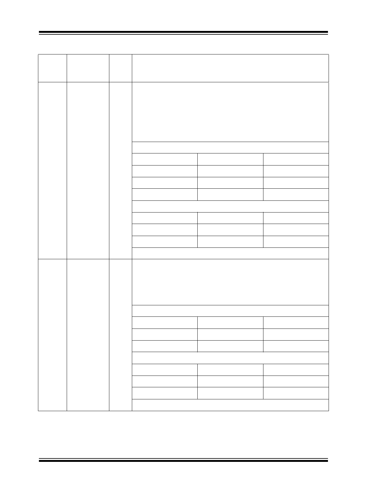
KSZ8091MLX
DS00002297A-page 8
2016 Microchip Technology Inc.
42
LED0/
PME_N1/
NWAYEN
Ipu/O
LED Output: Programmable LED0 Output.
PME_N Output: Programmable PME_N Output (pin option 1)
In this mode, this pin has a weak pull-up, is an open-drain, and requires an
external 1.0 kΩ pull-up resistor to VDDIO (digital V
DD
).
Config. Mode: Latched as auto-negotiation enable (Register 0h, Bit [12]) at
the de-assertion of reset. See the
Strap-In Options
section for details.
The LED0 pin is programmable using Register 1Fh, Bits [5:4], and is defined
as follows.
LED Mode = [00]
Link/Activity
Pin State
LED Definition
No Link
High
OFF
Link
Low
ON
Activity
Toggle
Blinking
LED Mode = [01]
Link
Pin State
LED Definition
No Link
High
OFF
Link
Low
ON
LED Mode = [10], [11]:
Reserved
43
LED1/
SPEED
Ipu/O
LED Output: Programmable LED1 output
Config. Mode: Latched as Speed (Register 0h, Bit [13]) at the de-assertion of
reset.
See the
Strap-In Options
section for details.
The LED1 pin is programmable using Register 1Fh, Bits [5:4], and is defined
as follows.
LED Mode = [00]
Speed
Pin State
LED Definition
10BASE-T
High
OFF
100BASE-TX
Low
ON
LED Mode = [01]
Activity
Pin State
LED Definition
No Activity
High
OFF
Activity
Toggle
Blinking
LED Mode = [10], [11]:
Reserved
TABLE 2-1:
SIGNALS - KSZ8091MLX (CONTINUED)
Pin
Number
Pin
Name
Type
Note
2-1
Description
2016 Microchip Technology Inc.
DS00002297A-page 9
KSZ8091MLX
Note 2-1
P = power supply
GND = ground
I = input
O = output
I/O = bi-directional
Ipu = Input with internal pull-up (see
Electrical Characteristics
for value).
Ipd = Input with internal pull-down (see
Electrical Characteristics
for value).
Ipu/O = Input with internal pull-up (see
Electrical Characteristics
for value) during power-up/reset;
output pin otherwise.
Ipd/O = Input with internal pull-down (see
Electrical Characteristics
for value) during power-up/reset;
output pin otherwise.
Ipu/Opu = Input with internal pull-up (see
Electrical Characteristics
for value) and output with internal
pull-up (see
Electrical Characteristics
for value).
Note 2-2
MII RX Mode: The RXD[3:0] bits are synchronous with RXC. When RXDV is asserted, RXD[3:0]
presents valid data to the MAC.
Note 2-3
MII TX Mode: The TXD[3:0] bits are synchronous with TXC. When TXEN is asserted, TXD[3:0]
presents valid data from the MAC.
44
TXER
Ipd
MII Mode: MII Transmit Error Input.
For EEE mode, this pin is driven by the EEE-MAC to put the KSZ8091MLX
transmit into the LPI state.
For non-EEE mode, this pin is not defined for error transmission from MAC to
KSZ8091MLX and can be left as a no connect.
For NAND_Tree mode, this pin should be pulled up by a pull-up resistor.
45
NC
—
No Connect. This pin is not bonded and can be left floating.
46
NC
—
No Connect. This pin is not bonded and can be left floating.
47
RST#
Ipu
Chip Reset (active-low).
48
NC
—
No Connect. This pin is not bonded and can be left floating.
TABLE 2-1:
SIGNALS - KSZ8091MLX (CONTINUED)
Pin
Number
Pin
Name
Type
Note
2-1
Description
KSZ8091MLX
DS00002297A-page 10
2016 Microchip Technology Inc.
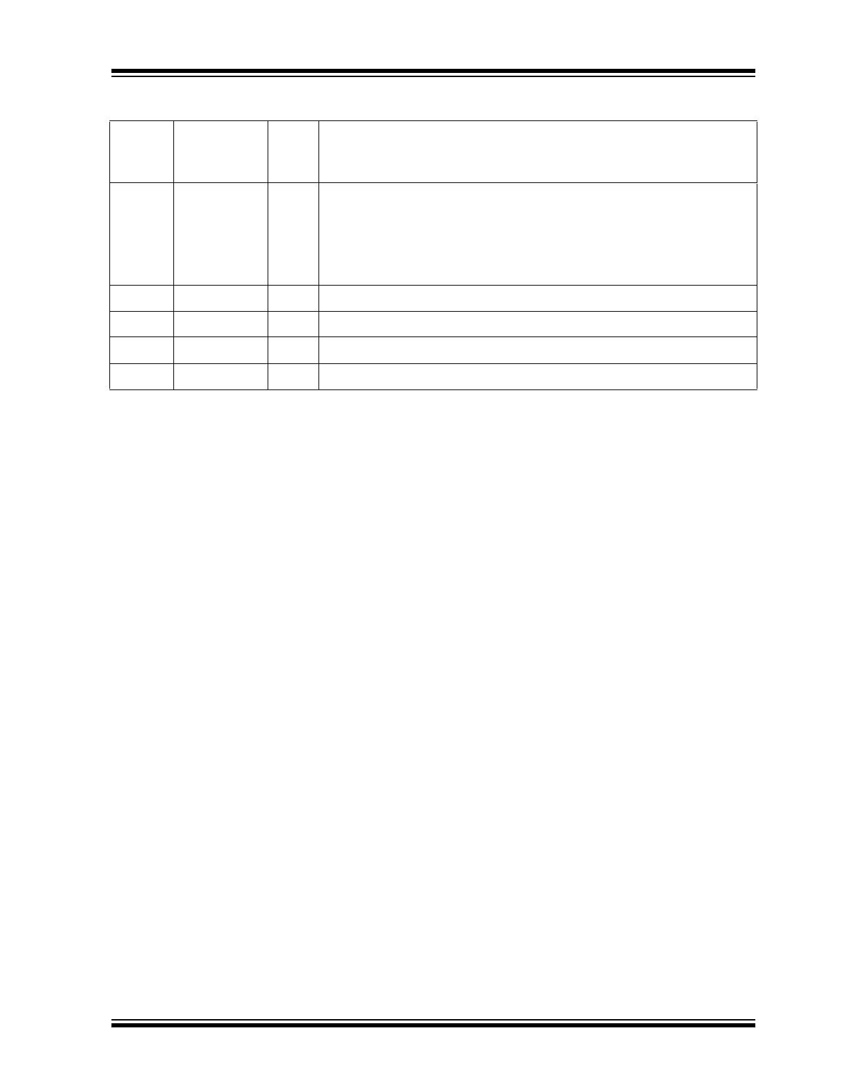
2.1
Strap-In Options
The strap-in pins are latched at the de-assertion of reset. In some systems, the MAC MII receive input pins may drive
high/low during power-up or reset, and consequently cause the PHY strap-in pins on the MII signals to be latched to
unintended high/low states. In this case, external pull-ups (4.7 kΩ) or pull-downs (1.0 kΩ) should be added on these
PHY strap-in pins to ensure that the intended values are strapped-in correctly.
TABLE 2-2:
STRAP-IN OPTIONS - KSZ8091MLX
Pin Number
Pin Name
Type
Note 2-4
Description
22
PHYAD2
Ipd/O
PHYAD[2:0] is latched at de-assertion of reset and is configurable to
any value from 0 to 7 with PHY Address 1 as the default value.
PHY Address 0 is assigned by default as the broadcast PHY
address, but it can be assigned as a unique PHY address after pull-
ing the B-CAST_OFF strapping pin high or writing a ‘1’ to Register
16h, bit [9].
PHY Address bits [4:3] are set to 00 by default.
21
PHYAD1
Ipd/O
20
PHYAD0
Ipu/O
27
CONFIG2
Ipd/O
The CONFIG[2:0] strap-in pins are latched at the de-assertion of
reset.
41
CONFIG1
CONFIG[2:0] Mode
000
MII (default)
40
CONFIG0
110
MII back-to-back
001 – 101,
111
Reserved, not used
33
PME_EN
Ipd/O
PME output for Wake-on-LAN
Pull-up = Enable
Pull-down (default) = Disable
At the de-assertion of reset, this pin value is latched into Register
16h, bit [15].
29
ISO
Ipd/O
Isolate mode
Pull-up = Enable
Pull-down (default) = Disable
At the de-assertion of reset, this pin value is latched into Register 0h,
bit [10].
43
SPEED
Ipu/O
Speed Mode:
Pull-up (default) = 100 Mbps
Pull-down = 10 Mbps
At the de-assertion of reset, this pin value is latched into Register 0h,
Bit [13] as the speed select, and also is latched into Register 4h
(Auto-Negotiation advertisement) as the speed capability support.
23
DUPLEX
Ipu/O
Duplex Mode:
Pull-up (default) = Half-duplex
Pull-down = Full-duplex
At the de-assertion of reset, this pin value is latched into Register 0h,
Bit [8].
42
NWAYEN
Ipu/O
Nway Auto-Negotiation Enable:
Pull-up (default) = Enable auto-negotiation
Pull-down = Disable auto-negotiation
At the de-assertion of reset, this pin value is latched into Register 0h,
Bit [12].
28
B-CAST_OFF
Ipd/O
Broadcast Off – for PHY Address 0:
Pull-up = PHY Address 0 is set as an unique PHY address
Pull-down (default) = PHY Address 0 is set as a broadcast PHY
address
At the de-assertion of reset, this pin value is latched by the chip.