
1
Features
•
Utilizes the AVR
®
RISC Architecture
•
AVR – High-performance and Low-power RISC Architecture
– 90 Powerful Instructions – Most Single Clock Cycle Execution
– 32 x 8 General-purpose Working Registers
– Up to 4 MIPS Throughput at 4 MHz
•
Nonvolatile Program Memory
– 2K Bytes of Flash Program Memory
– Endurance: 1,000 Write/Erase Cycles
– Programming Lock for Flash Program Data Security
•
Peripheral Features
– Interrupt and Wake-up on Low-level Input
– One 8-bit Timer/Counter with Separate Prescaler
– On-chip Analog Comparator
– Programmable Watchdog Timer with On-chip Oscillator
– Built-in High-current LED Driver with Programmable Modulation
•
Special Microcontroller Features
– Low-power Idle and Power-down Modes
– External and Internal Interrupt Sources
– Power-on Reset Circuit with Programmable Start-up Time
– Internal Calibrated RC Oscillator
•
Power Consumption at 1 MHz, 2V, 25
°C
– Active: 3.0 mA
– Idle Mode: 1.2 mA
– Power-down Mode: <1 µA
•
I/O and Packages
– 11 Programmable I/O Lines, 8 Input Lines and a High-current LED Driver
– 28-lead PDIP, 32-lead TQFP, and 32-pad MLF
•
Operating Voltages
– V
CC
: 1.8V - 5.5V for the ATtiny28V
– V
CC
: 2.7V - 5.5V for the ATtiny28L
•
Speed Grades
– 0 - 1.2 MHz for the ATtiny28V
– 0 - 4 MHz For the ATtiny28L
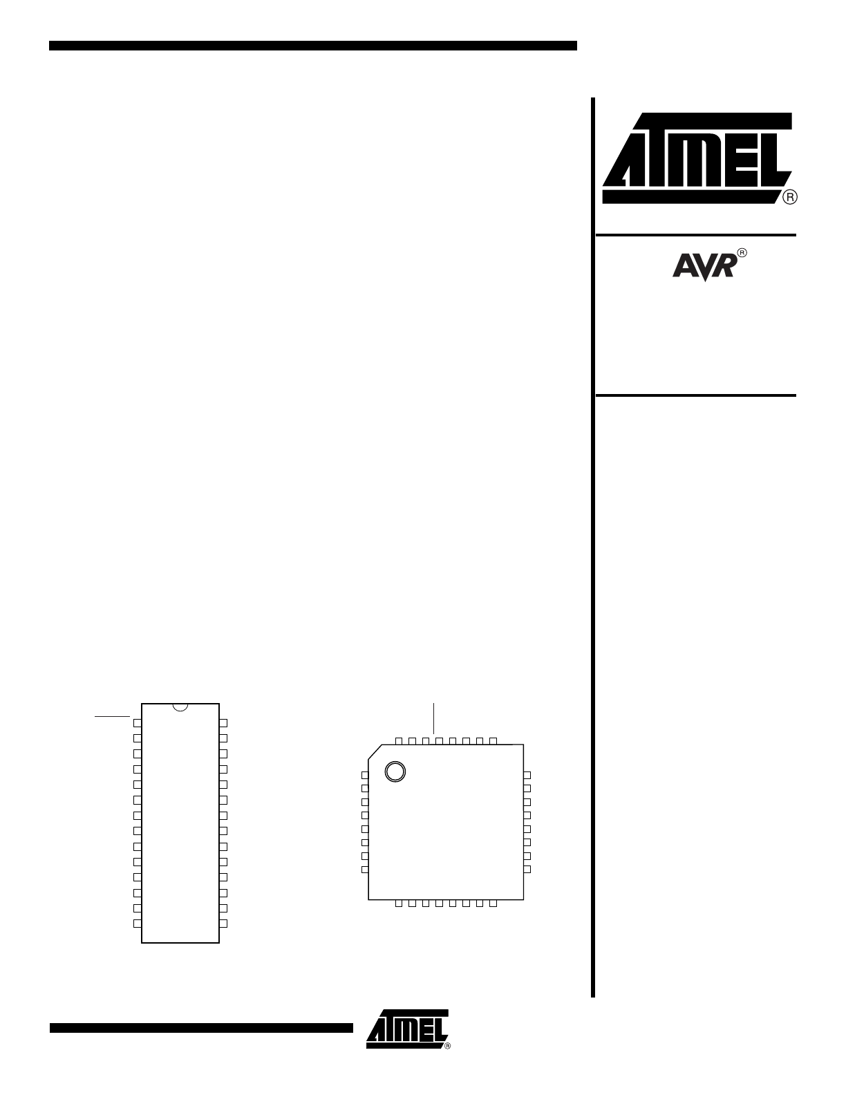
Pin Configurations
PDIP
RESET
PD0
PD1
PD2
PD3
PD4
VCC
GND
XTAL1
XTAL2
PD5
PD6
PD7
(AIN0) PB0
PA0
PA1
PA3
PA2 (IR)
PB7
PB6
GND
NC
VCC
PB5
PB4 (INT1)
PB3 (INT0)
PB2 (T0)
PB1 (AIN1)
1
2
3
4
5
6
7
8
9
10
11
12
13
14
28
27
26
25
24
23
22
21
20
19
18
17
16
15
TQFP/QFN/MLF
1
2
3
4
5
6
7
8
24
23
22
21
20
19
18
17
PD3
PD4
NC
VCC
GND
NC
XTAL1
XTAL2
PB7
PB6
NC
GND
NC
NC
VCC
PB5
32
31
30
29
28
27
26
25
9
10
11
12
13
14
15
16
PD5
PD6
PD7
(AIN0) PB0
(AIN1) PB1
(T0) PB2
(INT0) PB3
(INT1) PB4
PD2
PD1
PD0
RESET
PA0
PA1
PA3
PA2 (IR)
8-bit
Microcontroller
with 2K Bytes of
Flash
ATtiny28L
ATtiny28V
Summary
Rev. 1062FS–AVR–07/06
Note: This is a summary document. A complete document
is available on our Web site at www.atmel.com.
2
ATtiny28L/V
1062FS–AVR–07/06
Description
The ATtiny28 is a low-power CMOS 8-bit microcontroller based on the AVR RISC archi-
tecture. By executing powerful instructions in a single clock cycle, the ATtiny28 achieves
throughputs approaching 1 MIPS per MHz, allowing the system designer to optimize
power consumption versus processing speed. The AVR core combines a rich instruction
set with 32 general-purpose working registers. All the 32 registers are directly con-
nected to the Arithmetic Logic Unit (ALU), allowing two independent registers to be
accessed in one single instruction executed in one clock cycle. The resulting architec-
ture is more code efficient while achieving throughputs up to ten times faster than
conventional CISC microcontrollers.
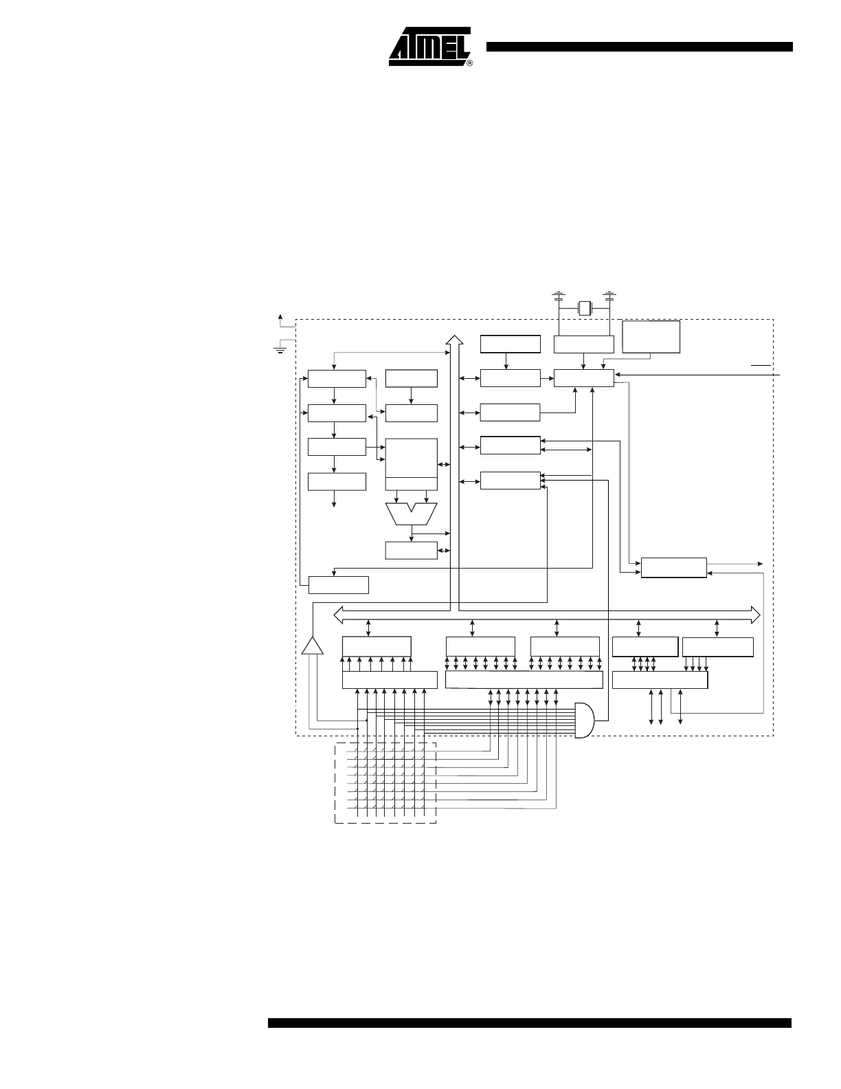
Block Diagram
Figure 1. The ATtiny28 Block Diagram
The ATtiny28 provides the following features: 2K bytes of Flash, 11 general-purpose I/O
lines, 8 input lines, a high-current LED driver, 32 general-purpose working registers, an
8-bit timer/counter, internal and external interrupts, programmable Watchdog Timer with
internal oscillator and 2 software-selectable power-saving modes. The Idle Mode stops
the CPU while allowing the timer/counter and interrupt system to continue functioning.
The Power-down mode saves the register contents but freezes the oscillator, disabling
all other chip functions until the next interrupt or hardware reset. The wake-up or inter-
PROGRAM
COUNTER
INTERNAL
OSCILLATOR
WATCHDOG
TIMER
STACK
POINTER
PROGRAM
FLASH
MCU CONTROL
REGISTER
GENERAL
PURPOSE
REGISTERS
INSTRUCTION
REGISTER
TIMER/
COUNTER
INSTRUCTION
DECODER
DATA REGISTER
PORTB
PROGRAMMING
LOGIC
TIMING AND
CONTROL
INTERRUPT
UNIT
STATUS
REGISTER
ALU
PORTB
VCC
GND
CONTROL
LINES
+
-
ANALOG
COMPARATOR
8-BIT DATA BUS
Z
OSCILLATOR
PORTD
DATA REGISTER
PORTA
PORTA
PORTA CONTROL
REGISTER
XTAL2
XTAL1
RESET
HARDWARE
STACK
DATA REGISTER
PORTD
DATA DIR
REG. PORTD
HARDWARE
MODULATOR
INTERNAL
CALIBRATED
OSCILLATOR

3
ATtiny28L/V
1062FS–AVR–07/06
rupt on low-level input feature enables the ATtiny28 to be highly responsive to external
events, still featuring the lowest power consumption while in the power-down modes.
The device is manufactured using Atmel’s high-density, nonvolatile memory technology.
By combining an enhanced RISC 8-bit CPU with Flash on a monolithic chip, the Atmel
ATtiny28 is a powerful microcontroller that provides a highly flexible and cost-effective
solution to many embedded control applications. The ATtiny28 AVR is supported with a
full suite of program and system development tools including: macro assemblers, pro-
gram debugger/simulators, in-circuit emulators and evaluation kits.
Pin Descriptions
VCC
Supply voltage pin.
GND
Ground pin.
Port A (PA3..PA0)
Port A is a 4-bit I/O port. PA2 is output-only and can be used as a high-current LED
driver. At V
CC
= 2.0V, the PA2 output buffer can sink 25 mA. PA3, PA1 and PA0 are
bi-directional I/O pins with internal pull-ups (selected for each bit). The port pins are tri-
stated when a reset condition becomes active, even if the clock is not running.
Port B (PB7..PB0)
Port B is an 8-bit input port with internal pull-ups (selected for all Port B pins). Port B
pins that are externally pulled low will source current if the pull-ups are activated.
Port B also serves the functions of various special features of the ATtiny28 as listed on
page 27. If any of the special features are enabled, the pull-up(s) on the corresponding
pin(s) is automatically disabled. The port pins are tri-stated when a reset condition
becomes active, even if the clock is not running.
Port D (PD7..PD0)
Port D is an 8-bit I/O port. Port pins can provide internal pull-up resistors (selected for
each bit). The port pins are tri-stated when a reset condition becomes active, even if the
clock is not running.
XTAL1
Input to the inverting oscillator amplifier and input to the internal clock operating circuit.
XTAL2
Output from the inverting oscillator amplifier.
RESET
Reset input. An external reset is generated by a low level on the RESET pin. Reset
pulses longer than 50 ns will generate a reset, even if the clock is not running. Shorter
pulses are not guaranteed to generate a reset.
4
ATtiny28L/V
1062FS–AVR–07/06
Notes:
1. For compatibility with future devices, reserved bits should be written to zero if accessed. Reserved I/O memory addresses
should never be written.
2. Some of the status flags are cleared by writing a logical “1” to them. Note that the CBI and SBI instructions will operate on all
bits in the I/O register, writing a one back into any flag read as set, thus clearing the flag. The CBI and SBI instructions work
with registers $00 to $1F only.
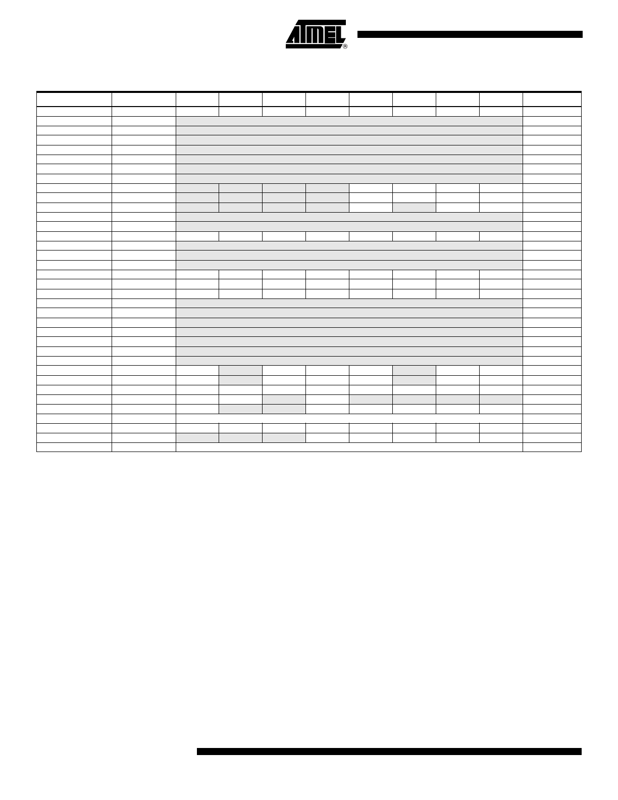
Register Summary
Address
Name
Bit 7
Bit 6
Bit 5
Bit 4
Bit 3
Bit 2
Bit 1
Bit 0
Page
$3F
SREG
I
T
H
S
V
N
Z
C
page 6
$3E
Reserved
...
Reserved
$20
Reserved
$1F
Reserved
$1E
Reserved
$1D
Reserved
$1C
Reserved
$1B
PORTA
-
-
-
-
PORTA3
PORTA2
PORTA1
PORTA0
page 32
$1A
PACR
-
-
-
-
DDA3
PA2HC
DDA1
DDA0
page 32
$19
PINA
-
-
-
-
PINA3
-
PINA1
PINA0
page 32
$18
Reserved
$17
Reserved
$16
PINB
PINB7
PINB6
PINB5
PINB4
PINB3
PINB2
PINB1
PINB0
page 32
$15
Reserved
$14
Reserved
$13
Reserved
$12
PORTD
PORTD7
PORTD6
PORTD5
PORTD4
PORTD3
PORTD2
PORTD1
PORTD0
page 33
$11
DDRD
DDD7
DDD6
DDD5
DDD4
DDD3
DDD2
DDD1
DDD0
page 33
$10
PIND
PIND7
PIND6
PIND5
PIND4
PIND3
PIND2
PIND1
PIND0
page 33
$0F
Reserved
$0E
Reserved
$0D
Reserved
$0C
Reserved
$0B
Reserved
$0A
Reserved
$09
Reserved
$08
ACSR
ACD
-
ACO
ACI
ACIE
-
ACIS1
ACIS0
page 44
$07
MCUCS
PLUPB
-
SE
SM
WDRF
-
EXTRF
PORF
page 19
$06
ICR
INT1
INT0
LLIE
TOIE0
ISC11
ISC10
ISC01
ISC00
page 22
$05
IFR
INTF1
INTF0
-
TOV0
-
-
-
-
page 23
$04
TCCR0
FOV0
-
-
OOM01
OOM00
CS02
CS01
CS00
page 35
$03
TCNT0
Timer/Counter0 (8-bit)
page 36
$02
MODCR
ONTIM4
ONTIM3
ONTIM2
ONTIM1
ONTIM0
MCONF2
MCONF1
MCONF0
page 43
$01
WDTCR
-
-
-
WDTOE
WDE
WDP2
WDP1
WDP0
page 37
$00
OSCCAL
Oscillator Calibration Register
page 9
5
ATtiny28L/V
1062FS–AVR–07/06
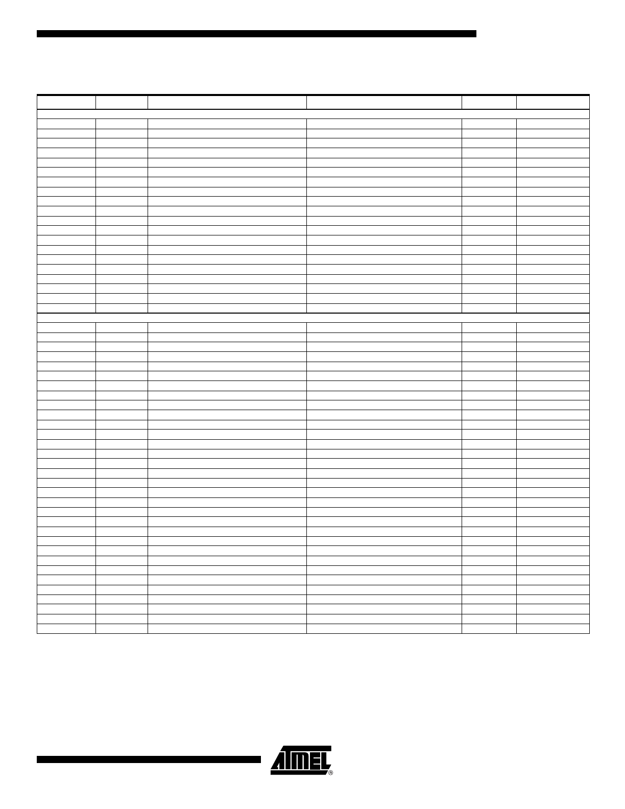
Instruction Set Summary
Mnemonic
Operands
Description
Operation
Flags
# Clocks
ARITHMETIC AND LOGIC INSTRUCTIONS
ADD
Rd, Rr
Add Two Registers
Rd
← Rd + Rr
Z,C,N,V,H
1
ADC
Rd, Rr
Add with Carry Two Registers
Rd
← Rd + Rr + C
Z,C,N,V,H
1
SUB
Rd, Rr
Subtract Two Registers
Rd
← Rd - Rr
Z,C,N,V,H
1
SUBI
Rd, K
Subtract Constant from Register
Rd
← Rd - K
Z,C,N,V,H
1
SBC
Rd, Rr
Subtract with Carry Two Registers
Rd
← Rd - Rr - C
Z,C,N,V,H
1
SBCI
Rd, K
Subtract with Carry Constant from Reg.
Rd
← Rd - K - C
Z,C,N,V,H
1
AND
Rd, Rr
Logical AND Registers
Rd
← Rd • Rr
Z,N,V
1
ANDI
Rd, K
Logical AND Register and Constant
Rd
← Rd • K
Z,N,V
1
OR
Rd, Rr
Logical OR Registers
Rd
← Rd v Rr
Z,N,V
1
ORI
Rd, K
Logical OR Register and Constant
Rd
← Rd v K
Z,N,V
1
EOR
Rd, Rr
Exclusive OR Registers
Rd
← Rd ⊕ Rr
Z,N,V
1
COM
Rd
One’s Complement
Rd
← $FF - Rd
Z,C,N,V
1
NEG
Rd
Two’s Complement
Rd
← $00 - Rd
Z,C,N,V,H
1
SBR
Rd, K
Set Bit(s) in Register
Rd
← Rd v K
Z,N,V
1
CBR
Rd, K
Clear Bit(s) in Register
Rd
← Rd • (FFh - K)
Z,N,V
1
INC
Rd
Increment
Rd
← Rd + 1
Z,N,V
1
DEC
Rd
Decrement
Rd
← Rd - 1
Z,N,V
1
TST
Rd
Test for Zero or Minus
Rd
← Rd • Rd Z,N,V
1
CLR
Rd
Clear Register
Rd
← Rd ⊕ Rd
Z,N,V
1
SER
Rd
Set Register
Rd
← $FF
None
1
BRANCH INSTRUCTIONS
RJMP
k
Relative Jump
PC
← PC + k + 1
None
2
RCALL
k
Relative Subroutine Call
PC
← PC + k + 1
None
3
RET
Subroutine Return
PC
← STACK
None
4
RETI
Interrupt Return
PC
← STACK
I
4
CPSE
Rd, Rr
Compare, Skip if Equal
if (Rd = Rr) PC
← PC + 2 or 3
None
1/2
CP
Rd, Rr
Compare
Rd - Rr
Z,N,V,C,H
1
CPC
Rd, Rr
Compare with Carry
Rd - Rr - C
Z,N,V,C,H
1
CPI
Rd, K
Compare Register with Immediate
Rd - K
Z N,V,C,H
1
SBRC
Rr, b
Skip if Bit in Register Cleared
if (Rr(b) = 0) PC
← PC + 2 or 3
None
1/2
SBRS
Rr, b
Skip if Bit in Register is Set
if (Rr(b) = 1) PC
← PC + 2 or 3
None
1/2
SBIC
P, b
Skip if Bit in I/O Register Cleared
if (P(b) = 0) PC
← PC + 2 or 3
None
1/2
SBIS
P, b
Skip if Bit in I/O Register is Set
if (P(b) = 1) PC
← PC + 2 or 3
None
1/2
BRBS
s, k
Branch if Status Flag Set
if (SREG(s) = 1) then PC
← PC + k + 1
None
1/2
BRBC
s, k
Branch if Status Flag Cleared
if (SREG(s) = 0) then PC
← PC + k + 1
None
1/2
BREQ
k
Branch if Equal
if (Z = 1) then PC
← PC + k + 1
None
1/2
BRNE
k
Branch if Not Equal
if (Z = 0) then PC
← PC + k + 1
None
1/2
BRCS
k
Branch if Carry Set
if (C = 1) then PC
← PC + k + 1
None
1/2
BRCC
k
Branch if Carry Cleared
if (C = 0) then PC
← PC + k + 1
None
1/2
BRSH
k
Branch if Same or Higher
if (C = 0) then PC
← PC + k + 1
None
1/2
BRLO
k
Branch if Lower
if (C = 1) then PC
← PC + k + 1
None
1/2
BRMI
k
Branch if Minus
if (N = 1) then PC
← PC + k + 1
None
1/2
BRPL
k
Branch if Plus
if (N = 0) then PC
← PC + k + 1
None
1/2
BRGE
k
Branch if Greater or Equal, Signed
if (N
⊕ V = 0) then PC ← PC + k + 1
None
1/2
BRLT
k
Branch if Less than Zero, Signed
if (N
⊕ V = 1) then PC ← PC + k + 1
None
1/2
BRHS
k
Branch if Half-carry Flag Set
if (H = 1) then PC
← PC + k + 1
None
1/2
BRHC
k
Branch if Half-carry Flag Cleared
if (H = 0) then PC
← PC + k + 1
None
1/2
BRTS
k
Branch if T-flag Set
if (T = 1) then PC
← PC + k + 1
None
1/2
BRTC
k
Branch if T-flag Cleared
if (T = 0) then PC
← PC + k + 1
None
1/2
BRVS
k
Branch if Overflow Flag is Set
if (V = 1) then PC
← PC + k + 1
None
1/2
BRVC
k
Branch if Overflow Flag is Cleared
if (V = 0) then PC
← PC + k + 1
None
1/2
BRIE
k
Branch if Interrupt Enabled
if (I = 1) then PC
← PC + k + 1
None
1/2
BRID
k
Branch if Interrupt Disabled
if (I = 0) then PC
← PC + k + 1
None
1/2
6
ATtiny28L/V
1062FS–AVR–07/06
DATA TRANSFER INSTRUCTIONS
LD
Rd, Z
Load Register Indirect
Rd
← (Z)
None
2
ST
Z, Rr
Store Register Indirect
(Z)
← Rr
None
2
MOV
Rd, Rr
Move between Registers
Rd
← Rr
None
1
LDI
Rd, K
Load Immediate
Rd
← K
None
1
IN
Rd, P
In Port
Rd
← P
None
1
OUT
P, Rr
Out Port
P
← Rr
None
1
LPM
Load Program Memory
R0
← (Z)
None
3
BIT AND BIT-TEST INSTRUCTIONS
SBI
P, b
Set Bit in I/O Register
I/O(P,b)
← 1
None
2
CBI
P, b
Clear Bit in I/O Register
I/O(P,b)
← 0
None
2
LSL
Rd
Logical Shift Left
Rd(n+1)
← Rd(n), Rd(0) ← 0
Z,C,N,V
1
LSR
Rd
Logical Shift Right
Rd(n)
← Rd(n+1), Rd(7) ← 0
Z,C,N,V
1
ROL
Rd
Rotate Left through Carry
Rd(0)
← C, Rd(n+1) ← Rd(n), C ← Rd(7)
Z,C,N,V
1
ROR
Rd
Rotate Right through Carry
Rd(7)
← C, Rd(n) ← Rd(n+1), C ← Rd(0)
Z,C,N,V
1
ASR
Rd
Arithmetic Shift Right
Rd(n)
← Rd(n+1), n = 0..6
Z,C,N,V
1
SWAP
Rd
Swap Nibbles
Rd(3..0)
← Rd(7..4), Rd(7..4) ← Rd(3..0)
None
1
BSET
s
Flag Set
SREG(s)
← 1
SREG(s)
1
BCLR
s
Flag Clear
SREG(s)
← 0
SREG(s)
1
BST
Rr, b
Bit Store from Register to T
T
← Rr(b)
T
1
BLD
Rd, b
Bit Load from T to Register
Rd(b)
← T
None
1
SEC
Set Carry
C
← 1
C
1
CLC
Clear Carry
C
← 0
C
1
SEN
Set Negative Flag
N
← 1
N
1
CLN
Clear Negative Flag
N
← 0
N
1
SEZ
Set Zero Flag
Z
← 1
Z
1
CLZ
Clear Zero Flag
Z
← 0
Z
1
SEI
Global Interrupt Enable
I
← 1
I
1
CLI
Global Interrupt Disable
I
← 0
I
1
SES
Set Signed Test Flag
S
← 1
S
1
CLS
Clear Signed Test Flag
S
← 0
S
1
SEV
Set Two’s Complement Overflow
V
← 1
V
1
CLV
Clear Two’s Complement Overflow
V
← 0
V
1
SET
Set T in SREG
T
← 1
T
1
CLT
Clear T in SREG
T
← 0
T
1
SEH
Set Half-carry Flag in SREG
H
← 1
H
1
CLH
Clear Half-carry Flag in SREG
H
← 0
H
1
NOP
No Operation
None
1
SLEEP
Sleep
(see specific descr. for Sleep function)
None
1
WDR
Watchdog Reset
(see specific descr. for WDR/timer)
None
1
Instruction Set Summary (Continued)
Mnemonic
Operands
Description
Operation
Flags
# Clocks

7
ATtiny28L/V
1062FS–AVR–07/06
Notes:
1. This device can also be supplied in wafer form. Please contact your local Atmel sales office for detailed ordering information
and minimum quantities.
2. Pb-free packaging alternative, complies to the European Directive for Restriction of Hazardous Substances (RoHS direc-
tive).Also Halide free and fully Green.
Ordering Information
Speed (MHz)
Power Supply (Volts)
Ordering Code
Package
(1)
Operation Range
4
2.7 - 5.5
ATtiny28L-4AC
ATtiny28L-4PC
ATtiny28L-4MC
32A
28P3
32M1-A
Commercial
(0
°C to 70°C)
ATtiny28L-4AI
ATtiny28L-4AU
(2)
ATtiny28L-4PI
ATtiny28L-4PU
(2)
ATtiny28L-4MI
ATtiny28L-4MU
(2)
32A
32A
28P3
28P3
32M1-A
32M1-A
Industrial
(-40
°C to 85°C)
1.2
1.8 - 5.5
ATtiny28V-1AC
ATtiny28V-1PC
ATtiny28V-1MC
32A
28P3
32M1-A
Commercial
(0
°C to 70°C)
ATtiny28V-1AI
ATtiny28V-1AU
(2)
ATtiny28V-1PI
ATtiny28V-1PU
(2)
ATtiny28V-1MI
ATtiny28V-1MU
(2)
32A
32A
28P3
28P3
32M1-A
32M1-A
Industrial
(-40
°C to 85°C)
Package Type
32A
32-lead, Thin (1.0 mm) Plastic Quad Flat Package (TQFP)
28P3
28-lead, 0.300" Wide, Plastic Dual Inline Package (PDIP)
32M1-A
32-pad, 5x5x1.0 body, Lead Pitch 0.50mm, Quad Flat No-lead/Micro Lead Frame Package (QFN/MLF)
8
ATtiny28L/V
1062FS–AVR–07/06
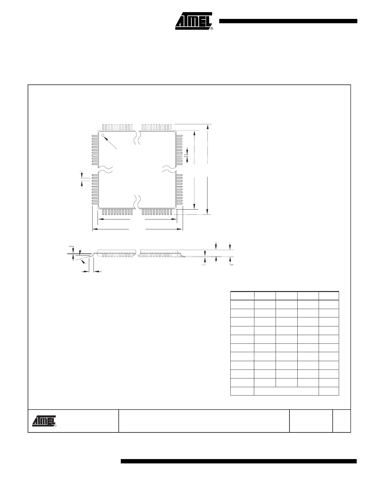
Packaging Information
32A
2325 Orchard Parkway
San Jose, CA 95131
TITLE
DRAWING NO.
R
REV.
32A, 32-lead, 7 x 7 mm Body Size, 1.0 mm Body Thickness,
0.8 mm Lead Pitch, Thin Profile Plastic Quad Flat Package (TQFP)
B
32A
10/5/2001
PIN 1 IDENTIFIER
0˚~7˚
PIN 1
L
C
A1
A2
A
D1
D
e
E1
E
B
Notes:
1. This package conforms to JEDEC reference MS-026, Variation ABA.
2. Dimensions D1 and E1 do not include mold protrusion. Allowable
protrusion is 0.25 mm per side. Dimensions D1 and E1 are maximum
plastic body size dimensions including mold mismatch.
3. Lead coplanarity is 0.10 mm maximum.
A
–
–
1.20
A1
0.05
–
0.15
A2
0.95
1.00
1.05
D
8.75
9.00
9.25
D1
6.90
7.00
7.10
Note 2
E
8.75
9.00
9.25
E1
6.90
7.00
7.10
Note 2
B 0.30
–
0.45
C
0.09
–
0.20
L
0.45
–
0.75
e
0.80 TYP
COMMON DIMENSIONS
(Unit of Measure = mm)
SYMBOL
MIN
NOM
MAX
NOTE
9
ATtiny28L/V
1062FS–AVR–07/06
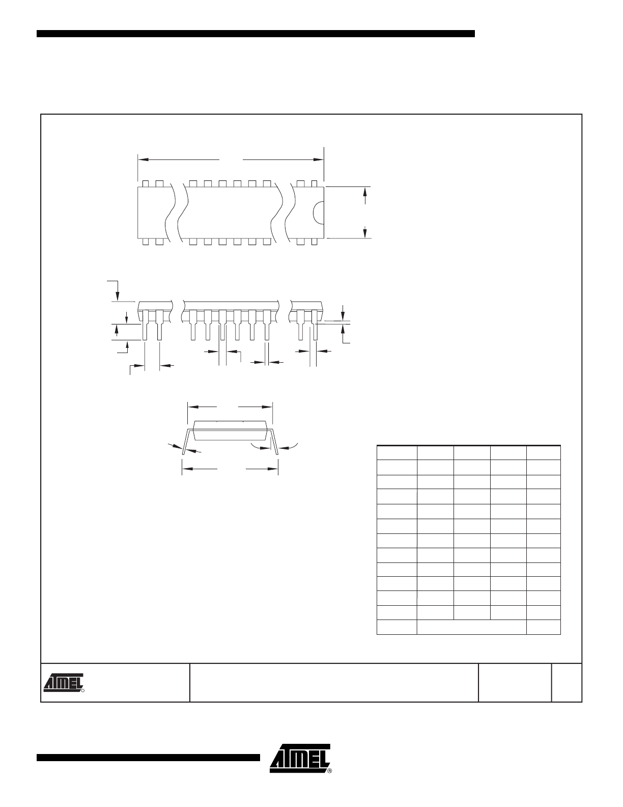
28P3
2325 Orchard Parkway
San Jose, CA 95131
TITLE
DRAWING NO.
R
REV.
28P3, 28-lead (0.300"/7.62 mm Wide) Plastic Dual
Inline Package (PDIP)
B
28P3
09/28/01
PIN
1
E1
A1
B
REF
E
B1
C
L
SEATING PLANE
A
0º ~ 15º
D
e
eB
B2
(4 PLACES)
COMMON DIMENSIONS
(Unit of Measure = mm)
SYMBOL
MIN
NOM
MAX
NOTE
A
–
–
4.5724
A1
0.508
–
–
D
34.544
– 34.798 Note 1
E
7.620
–
8.255
E1
7.112
–
7.493
Note 1
B
0.381
–
0.533
B1
1.143
–
1.397
B2
0.762
–
1.143
L
3.175
–
3.429
C
0.203
–
0.356
eB
–
–
10.160
e 2.540 TYP
Note:
1. Dimensions D and E1 do not include mold Flash or Protrusion.
Mold Flash or Protrusion shall not exceed 0.25 mm (0.010").
10
ATtiny28L/V
1062FS–AVR–07/06
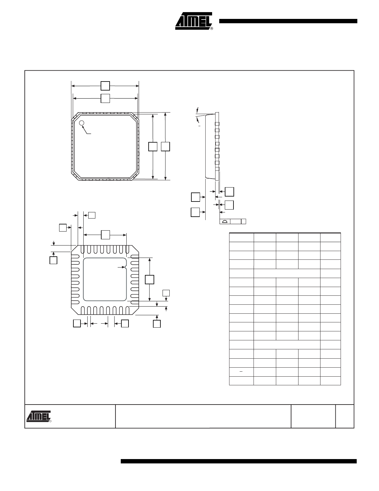
32M1-A
2325 Orchard Parkway
San Jose, CA 95131
TITLE
DRAWING NO.
R
REV.
32M1-A, 32-pad, 5 x 5 x 1.0 mm Body, Lead Pitch 0.50 mm,
E
32M1-A
5/25/06
3.10 mm Exposed Pad, Micro Lead Frame Package (MLF)
COMMON DIMENSIONS
(Unit of Measure = mm)
SYMBOL
MIN
NOM
MAX
NOTE
D1
D
E1
E
e
b
A3
A2
A1
A
D2
E2
0.08 C
L
1
2
3
P
P
0
1
2
3
A
0.80
0.90
1.00
A1
–
0.02
0.05
A2
–
0.65
1.00
A3
0.20 REF
b
0.18
0.23
0.30
D
D1
D2
2.95
3.10
3.25
4.90
5.00
5.10
4.70
4.75
4.80
4.70
4.75
4.80
4.90
5.00
5.10
E
E1
E2
2.95
3.10
3.25
e
0.50 BSC
L
0.30
0.40
0.50
P
–
–
0.60
–
–
12
o
Note: JEDEC Standard MO-220, Fig. 2 (Anvil Singulation), VHHD-2.
TOP VIEW
SIDE VIEW
BOTTOM VIEW
0
Pin 1 ID
Pin #1 Notch
(0.20 R)
K
0.20
–
–
K
K
1
Features
•
Utilizes the AVR
®
RISC Architecture
•
AVR – High-performance and Low-power RISC Architecture
– 90 Powerful Instructions – Most Single Clock Cycle Execution
– 32 x 8 General-purpose Working Registers
– Up to 4 MIPS Throughput at 4 MHz
•
Nonvolatile Program Memory
– 2K Bytes of Flash Program Memory
– Endurance: 1,000 Write/Erase Cycles
– Programming Lock for Flash Program Data Security
•
Peripheral Features
– Interrupt and Wake-up on Low-level Input
– One 8-bit Timer/Counter with Separate Prescaler
– On-chip Analog Comparator
– Programmable Watchdog Timer with On-chip Oscillator
– Built-in High-current LED Driver with Programmable Modulation
•
Special Microcontroller Features
– Low-power Idle and Power-down Modes
– External and Internal Interrupt Sources
– Power-on Reset Circuit with Programmable Start-up Time
– Internal Calibrated RC Oscillator
•
Power Consumption at 1 MHz, 2V, 25
°C
– Active: 3.0 mA
– Idle Mode: 1.2 mA
– Power-down Mode: <1 µA
•
I/O and Packages
– 11 Programmable I/O Lines, 8 Input Lines and a High-current LED Driver
– 28-lead PDIP, 32-lead TQFP, and 32-pad MLF
•
Operating Voltages
– V
CC
: 1.8V - 5.5V for the ATtiny28V
– V
CC
: 2.7V - 5.5V for the ATtiny28L
•
Speed Grades
– 0 - 1.2 MHz for the ATtiny28V
– 0 - 4 MHz For the ATtiny28L
Pin Configurations
PDIP
RESET
PD0
PD1
PD2
PD3
PD4
VCC
GND
XTAL1
XTAL2
PD5
PD6
PD7
(AIN0) PB0
PA0
PA1
PA3
PA2 (IR)
PB7
PB6
GND
NC
VCC
PB5
PB4 (INT1)
PB3 (INT0)
PB2 (T0)
PB1 (AIN1)
1
2
3
4
5
6
7
8
9
10
11
12
13
14
28
27
26
25
24
23
22
21
20
19
18
17
16
15
TQFP/QFN/MLF
1
2
3
4
5
6
7
8
24
23
22
21
20
19
18
17
PD3
PD4
NC
VCC
GND
NC
XTAL1
XTAL2
PB7
PB6
NC
GND
NC
NC
VCC
PB5
32
31
30
29
28
27
26
25
9
10
11
12
13
14
15
16
PD5
PD6
PD7
(AIN0) PB0
(AIN1) PB1
(T0) PB2
(INT0) PB3
(INT1) PB4
PD2
PD1
PD0
RESET
PA0
PA1
PA3
PA2 (IR)
8-bit
Microcontroller
with 2K Bytes of
Flash
ATtiny28L
ATtiny28V
Summary
Rev. 1062FS–AVR–07/06
Note: This is a summary document. A complete document
is available on our Web site at www.atmel.com.
2
ATtiny28L/V
1062FS–AVR–07/06
Description
The ATtiny28 is a low-power CMOS 8-bit microcontroller based on the AVR RISC archi-
tecture. By executing powerful instructions in a single clock cycle, the ATtiny28 achieves
throughputs approaching 1 MIPS per MHz, allowing the system designer to optimize
power consumption versus processing speed. The AVR core combines a rich instruction
set with 32 general-purpose working registers. All the 32 registers are directly con-
nected to the Arithmetic Logic Unit (ALU), allowing two independent registers to be
accessed in one single instruction executed in one clock cycle. The resulting architec-
ture is more code efficient while achieving throughputs up to ten times faster than
conventional CISC microcontrollers.
Block Diagram
Figure 1. The ATtiny28 Block Diagram
The ATtiny28 provides the following features: 2K bytes of Flash, 11 general-purpose I/O
lines, 8 input lines, a high-current LED driver, 32 general-purpose working registers, an
8-bit timer/counter, internal and external interrupts, programmable Watchdog Timer with
internal oscillator and 2 software-selectable power-saving modes. The Idle Mode stops
the CPU while allowing the timer/counter and interrupt system to continue functioning.
The Power-down mode saves the register contents but freezes the oscillator, disabling
all other chip functions until the next interrupt or hardware reset. The wake-up or inter-
PROGRAM
COUNTER
INTERNAL
OSCILLATOR
WATCHDOG
TIMER
STACK
POINTER
PROGRAM
FLASH
MCU CONTROL
REGISTER
GENERAL
PURPOSE
REGISTERS
INSTRUCTION
REGISTER
TIMER/
COUNTER
INSTRUCTION
DECODER
DATA REGISTER
PORTB
PROGRAMMING
LOGIC
TIMING AND
CONTROL
INTERRUPT
UNIT
STATUS
REGISTER
ALU
PORTB
VCC
GND
CONTROL
LINES
+
-
ANALOG
COMPARATOR
8-BIT DATA BUS
Z
OSCILLATOR
PORTD
DATA REGISTER
PORTA
PORTA
PORTA CONTROL
REGISTER
XTAL2
XTAL1
RESET
HARDWARE
STACK
DATA REGISTER
PORTD
DATA DIR
REG. PORTD
HARDWARE
MODULATOR
INTERNAL
CALIBRATED
OSCILLATOR
3
ATtiny28L/V
1062FS–AVR–07/06
rupt on low-level input feature enables the ATtiny28 to be highly responsive to external
events, still featuring the lowest power consumption while in the power-down modes.
The device is manufactured using Atmel’s high-density, nonvolatile memory technology.
By combining an enhanced RISC 8-bit CPU with Flash on a monolithic chip, the Atmel
ATtiny28 is a powerful microcontroller that provides a highly flexible and cost-effective
solution to many embedded control applications. The ATtiny28 AVR is supported with a
full suite of program and system development tools including: macro assemblers, pro-
gram debugger/simulators, in-circuit emulators and evaluation kits.
Pin Descriptions
VCC
Supply voltage pin.
GND
Ground pin.
Port A (PA3..PA0)
Port A is a 4-bit I/O port. PA2 is output-only and can be used as a high-current LED
driver. At V
CC
= 2.0V, the PA2 output buffer can sink 25 mA. PA3, PA1 and PA0 are
bi-directional I/O pins with internal pull-ups (selected for each bit). The port pins are tri-
stated when a reset condition becomes active, even if the clock is not running.
Port B (PB7..PB0)
Port B is an 8-bit input port with internal pull-ups (selected for all Port B pins). Port B
pins that are externally pulled low will source current if the pull-ups are activated.
Port B also serves the functions of various special features of the ATtiny28 as listed on
page 27. If any of the special features are enabled, the pull-up(s) on the corresponding
pin(s) is automatically disabled. The port pins are tri-stated when a reset condition
becomes active, even if the clock is not running.
Port D (PD7..PD0)
Port D is an 8-bit I/O port. Port pins can provide internal pull-up resistors (selected for
each bit). The port pins are tri-stated when a reset condition becomes active, even if the
clock is not running.
XTAL1
Input to the inverting oscillator amplifier and input to the internal clock operating circuit.
XTAL2
Output from the inverting oscillator amplifier.
RESET
Reset input. An external reset is generated by a low level on the RESET pin. Reset
pulses longer than 50 ns will generate a reset, even if the clock is not running. Shorter
pulses are not guaranteed to generate a reset.
4
ATtiny28L/V
1062FS–AVR–07/06
Notes:
1. For compatibility with future devices, reserved bits should be written to zero if accessed. Reserved I/O memory addresses
should never be written.
2. Some of the status flags are cleared by writing a logical “1” to them. Note that the CBI and SBI instructions will operate on all
bits in the I/O register, writing a one back into any flag read as set, thus clearing the flag. The CBI and SBI instructions work
with registers $00 to $1F only.
Register Summary
Address
Name
Bit 7
Bit 6
Bit 5
Bit 4
Bit 3
Bit 2
Bit 1
Bit 0
Page
$3F
SREG
I
T
H
S
V
N
Z
C
page 6
$3E
Reserved
...
Reserved
$20
Reserved
$1F
Reserved
$1E
Reserved
$1D
Reserved
$1C
Reserved
$1B
PORTA
-
-
-
-
PORTA3
PORTA2
PORTA1
PORTA0
page 32
$1A
PACR
-
-
-
-
DDA3
PA2HC
DDA1
DDA0
page 32
$19
PINA
-
-
-
-
PINA3
-
PINA1
PINA0
page 32
$18
Reserved
$17
Reserved
$16
PINB
PINB7
PINB6
PINB5
PINB4
PINB3
PINB2
PINB1
PINB0
page 32
$15
Reserved
$14
Reserved
$13
Reserved
$12
PORTD
PORTD7
PORTD6
PORTD5
PORTD4
PORTD3
PORTD2
PORTD1
PORTD0
page 33
$11
DDRD
DDD7
DDD6
DDD5
DDD4
DDD3
DDD2
DDD1
DDD0
page 33
$10
PIND
PIND7
PIND6
PIND5
PIND4
PIND3
PIND2
PIND1
PIND0
page 33
$0F
Reserved
$0E
Reserved
$0D
Reserved
$0C
Reserved
$0B
Reserved
$0A
Reserved
$09
Reserved
$08
ACSR
ACD
-
ACO
ACI
ACIE
-
ACIS1
ACIS0
page 44
$07
MCUCS
PLUPB
-
SE
SM
WDRF
-
EXTRF
PORF
page 19
$06
ICR
INT1
INT0
LLIE
TOIE0
ISC11
ISC10
ISC01
ISC00
page 22
$05
IFR
INTF1
INTF0
-
TOV0
-
-
-
-
page 23
$04
TCCR0
FOV0
-
-
OOM01
OOM00
CS02
CS01
CS00
page 35
$03
TCNT0
Timer/Counter0 (8-bit)
page 36
$02
MODCR
ONTIM4
ONTIM3
ONTIM2
ONTIM1
ONTIM0
MCONF2
MCONF1
MCONF0
page 43
$01
WDTCR
-
-
-
WDTOE
WDE
WDP2
WDP1
WDP0
page 37
$00
OSCCAL
Oscillator Calibration Register
page 9
5
ATtiny28L/V
1062FS–AVR–07/06
Instruction Set Summary
Mnemonic
Operands
Description
Operation
Flags
# Clocks
ARITHMETIC AND LOGIC INSTRUCTIONS
ADD
Rd, Rr
Add Two Registers
Rd
← Rd + Rr
Z,C,N,V,H
1
ADC
Rd, Rr
Add with Carry Two Registers
Rd
← Rd + Rr + C
Z,C,N,V,H
1
SUB
Rd, Rr
Subtract Two Registers
Rd
← Rd - Rr
Z,C,N,V,H
1
SUBI
Rd, K
Subtract Constant from Register
Rd
← Rd - K
Z,C,N,V,H
1
SBC
Rd, Rr
Subtract with Carry Two Registers
Rd
← Rd - Rr - C
Z,C,N,V,H
1
SBCI
Rd, K
Subtract with Carry Constant from Reg.
Rd
← Rd - K - C
Z,C,N,V,H
1
AND
Rd, Rr
Logical AND Registers
Rd
← Rd • Rr
Z,N,V
1
ANDI
Rd, K
Logical AND Register and Constant
Rd
← Rd • K
Z,N,V
1
OR
Rd, Rr
Logical OR Registers
Rd
← Rd v Rr
Z,N,V
1
ORI
Rd, K
Logical OR Register and Constant
Rd
← Rd v K
Z,N,V
1
EOR
Rd, Rr
Exclusive OR Registers
Rd
← Rd ⊕ Rr
Z,N,V
1
COM
Rd
One’s Complement
Rd
← $FF - Rd
Z,C,N,V
1
NEG
Rd
Two’s Complement
Rd
← $00 - Rd
Z,C,N,V,H
1
SBR
Rd, K
Set Bit(s) in Register
Rd
← Rd v K
Z,N,V
1
CBR
Rd, K
Clear Bit(s) in Register
Rd
← Rd • (FFh - K)
Z,N,V
1
INC
Rd
Increment
Rd
← Rd + 1
Z,N,V
1
DEC
Rd
Decrement
Rd
← Rd - 1
Z,N,V
1
TST
Rd
Test for Zero or Minus
Rd
← Rd • Rd Z,N,V
1
CLR
Rd
Clear Register
Rd
← Rd ⊕ Rd
Z,N,V
1
SER
Rd
Set Register
Rd
← $FF
None
1
BRANCH INSTRUCTIONS
RJMP
k
Relative Jump
PC
← PC + k + 1
None
2
RCALL
k
Relative Subroutine Call
PC
← PC + k + 1
None
3
RET
Subroutine Return
PC
← STACK
None
4
RETI
Interrupt Return
PC
← STACK
I
4
CPSE
Rd, Rr
Compare, Skip if Equal
if (Rd = Rr) PC
← PC + 2 or 3
None
1/2
CP
Rd, Rr
Compare
Rd - Rr
Z,N,V,C,H
1
CPC
Rd, Rr
Compare with Carry
Rd - Rr - C
Z,N,V,C,H
1
CPI
Rd, K
Compare Register with Immediate
Rd - K
Z N,V,C,H
1
SBRC
Rr, b
Skip if Bit in Register Cleared
if (Rr(b) = 0) PC
← PC + 2 or 3
None
1/2
SBRS
Rr, b
Skip if Bit in Register is Set
if (Rr(b) = 1) PC
← PC + 2 or 3
None
1/2
SBIC
P, b
Skip if Bit in I/O Register Cleared
if (P(b) = 0) PC
← PC + 2 or 3
None
1/2
SBIS
P, b
Skip if Bit in I/O Register is Set
if (P(b) = 1) PC
← PC + 2 or 3
None
1/2
BRBS
s, k
Branch if Status Flag Set
if (SREG(s) = 1) then PC
← PC + k + 1
None
1/2
BRBC
s, k
Branch if Status Flag Cleared
if (SREG(s) = 0) then PC
← PC + k + 1
None
1/2
BREQ
k
Branch if Equal
if (Z = 1) then PC
← PC + k + 1
None
1/2
BRNE
k
Branch if Not Equal
if (Z = 0) then PC
← PC + k + 1
None
1/2
BRCS
k
Branch if Carry Set
if (C = 1) then PC
← PC + k + 1
None
1/2
BRCC
k
Branch if Carry Cleared
if (C = 0) then PC
← PC + k + 1
None
1/2
BRSH
k
Branch if Same or Higher
if (C = 0) then PC
← PC + k + 1
None
1/2
BRLO
k
Branch if Lower
if (C = 1) then PC
← PC + k + 1
None
1/2
BRMI
k
Branch if Minus
if (N = 1) then PC
← PC + k + 1
None
1/2
BRPL
k
Branch if Plus
if (N = 0) then PC
← PC + k + 1
None
1/2
BRGE
k
Branch if Greater or Equal, Signed
if (N
⊕ V = 0) then PC ← PC + k + 1
None
1/2
BRLT
k
Branch if Less than Zero, Signed
if (N
⊕ V = 1) then PC ← PC + k + 1
None
1/2
BRHS
k
Branch if Half-carry Flag Set
if (H = 1) then PC
← PC + k + 1
None
1/2
BRHC
k
Branch if Half-carry Flag Cleared
if (H = 0) then PC
← PC + k + 1
None
1/2
BRTS
k
Branch if T-flag Set
if (T = 1) then PC
← PC + k + 1
None
1/2
BRTC
k
Branch if T-flag Cleared
if (T = 0) then PC
← PC + k + 1
None
1/2
BRVS
k
Branch if Overflow Flag is Set
if (V = 1) then PC
← PC + k + 1
None
1/2
BRVC
k
Branch if Overflow Flag is Cleared
if (V = 0) then PC
← PC + k + 1
None
1/2
BRIE
k
Branch if Interrupt Enabled
if (I = 1) then PC
← PC + k + 1
None
1/2
BRID
k
Branch if Interrupt Disabled
if (I = 0) then PC
← PC + k + 1
None
1/2
6
ATtiny28L/V
1062FS–AVR–07/06
DATA TRANSFER INSTRUCTIONS
LD
Rd, Z
Load Register Indirect
Rd
← (Z)
None
2
ST
Z, Rr
Store Register Indirect
(Z)
← Rr
None
2
MOV
Rd, Rr
Move between Registers
Rd
← Rr
None
1
LDI
Rd, K
Load Immediate
Rd
← K
None
1
IN
Rd, P
In Port
Rd
← P
None
1
OUT
P, Rr
Out Port
P
← Rr
None
1
LPM
Load Program Memory
R0
← (Z)
None
3
BIT AND BIT-TEST INSTRUCTIONS
SBI
P, b
Set Bit in I/O Register
I/O(P,b)
← 1
None
2
CBI
P, b
Clear Bit in I/O Register
I/O(P,b)
← 0
None
2
LSL
Rd
Logical Shift Left
Rd(n+1)
← Rd(n), Rd(0) ← 0
Z,C,N,V
1
LSR
Rd
Logical Shift Right
Rd(n)
← Rd(n+1), Rd(7) ← 0
Z,C,N,V
1
ROL
Rd
Rotate Left through Carry
Rd(0)
← C, Rd(n+1) ← Rd(n), C ← Rd(7)
Z,C,N,V
1
ROR
Rd
Rotate Right through Carry
Rd(7)
← C, Rd(n) ← Rd(n+1), C ← Rd(0)
Z,C,N,V
1
ASR
Rd
Arithmetic Shift Right
Rd(n)
← Rd(n+1), n = 0..6
Z,C,N,V
1
SWAP
Rd
Swap Nibbles
Rd(3..0)
← Rd(7..4), Rd(7..4) ← Rd(3..0)
None
1
BSET
s
Flag Set
SREG(s)
← 1
SREG(s)
1
BCLR
s
Flag Clear
SREG(s)
← 0
SREG(s)
1
BST
Rr, b
Bit Store from Register to T
T
← Rr(b)
T
1
BLD
Rd, b
Bit Load from T to Register
Rd(b)
← T
None
1
SEC
Set Carry
C
← 1
C
1
CLC
Clear Carry
C
← 0
C
1
SEN
Set Negative Flag
N
← 1
N
1
CLN
Clear Negative Flag
N
← 0
N
1
SEZ
Set Zero Flag
Z
← 1
Z
1
CLZ
Clear Zero Flag
Z
← 0
Z
1
SEI
Global Interrupt Enable
I
← 1
I
1
CLI
Global Interrupt Disable
I
← 0
I
1
SES
Set Signed Test Flag
S
← 1
S
1
CLS
Clear Signed Test Flag
S
← 0
S
1
SEV
Set Two’s Complement Overflow
V
← 1
V
1
CLV
Clear Two’s Complement Overflow
V
← 0
V
1
SET
Set T in SREG
T
← 1
T
1
CLT
Clear T in SREG
T
← 0
T
1
SEH
Set Half-carry Flag in SREG
H
← 1
H
1
CLH
Clear Half-carry Flag in SREG
H
← 0
H
1
NOP
No Operation
None
1
SLEEP
Sleep
(see specific descr. for Sleep function)
None
1
WDR
Watchdog Reset
(see specific descr. for WDR/timer)
None
1
Instruction Set Summary (Continued)
Mnemonic
Operands
Description
Operation
Flags
# Clocks
7
ATtiny28L/V
1062FS–AVR–07/06
Notes:
1. This device can also be supplied in wafer form. Please contact your local Atmel sales office for detailed ordering information
and minimum quantities.
2. Pb-free packaging alternative, complies to the European Directive for Restriction of Hazardous Substances (RoHS direc-
tive).Also Halide free and fully Green.
Ordering Information
Speed (MHz)
Power Supply (Volts)
Ordering Code
Package
(1)
Operation Range
4
2.7 - 5.5
ATtiny28L-4AC
ATtiny28L-4PC
ATtiny28L-4MC
32A
28P3
32M1-A
Commercial
(0
°C to 70°C)
ATtiny28L-4AI
ATtiny28L-4AU
(2)
ATtiny28L-4PI
ATtiny28L-4PU
(2)
ATtiny28L-4MI
ATtiny28L-4MU
(2)
32A
32A
28P3
28P3
32M1-A
32M1-A
Industrial
(-40
°C to 85°C)
1.2
1.8 - 5.5
ATtiny28V-1AC
ATtiny28V-1PC
ATtiny28V-1MC
32A
28P3
32M1-A
Commercial
(0
°C to 70°C)
ATtiny28V-1AI
ATtiny28V-1AU
(2)
ATtiny28V-1PI
ATtiny28V-1PU
(2)
ATtiny28V-1MI
ATtiny28V-1MU
(2)
32A
32A
28P3
28P3
32M1-A
32M1-A
Industrial
(-40
°C to 85°C)
Package Type
32A
32-lead, Thin (1.0 mm) Plastic Quad Flat Package (TQFP)
28P3
28-lead, 0.300" Wide, Plastic Dual Inline Package (PDIP)
32M1-A
32-pad, 5x5x1.0 body, Lead Pitch 0.50mm, Quad Flat No-lead/Micro Lead Frame Package (QFN/MLF)
8
ATtiny28L/V
1062FS–AVR–07/06
Packaging Information
32A
2325 Orchard Parkway
San Jose, CA 95131
TITLE
DRAWING NO.
R
REV.
32A, 32-lead, 7 x 7 mm Body Size, 1.0 mm Body Thickness,
0.8 mm Lead Pitch, Thin Profile Plastic Quad Flat Package (TQFP)
B
32A
10/5/2001
PIN 1 IDENTIFIER
0˚~7˚
PIN 1
L
C
A1
A2
A
D1
D
e
E1
E
B
Notes:
1. This package conforms to JEDEC reference MS-026, Variation ABA.
2. Dimensions D1 and E1 do not include mold protrusion. Allowable
protrusion is 0.25 mm per side. Dimensions D1 and E1 are maximum
plastic body size dimensions including mold mismatch.
3. Lead coplanarity is 0.10 mm maximum.
A
–
–
1.20
A1
0.05
–
0.15
A2
0.95
1.00
1.05
D
8.75
9.00
9.25
D1
6.90
7.00
7.10
Note 2
E
8.75
9.00
9.25
E1
6.90
7.00
7.10
Note 2
B 0.30
–
0.45
C
0.09
–
0.20
L
0.45
–
0.75
e
0.80 TYP
COMMON DIMENSIONS
(Unit of Measure = mm)
SYMBOL
MIN
NOM
MAX
NOTE
9
ATtiny28L/V
1062FS–AVR–07/06
28P3
2325 Orchard Parkway
San Jose, CA 95131
TITLE
DRAWING NO.
R
REV.
28P3, 28-lead (0.300"/7.62 mm Wide) Plastic Dual
Inline Package (PDIP)
B
28P3
09/28/01
PIN
1
E1
A1
B
REF
E
B1
C
L
SEATING PLANE
A
0º ~ 15º
D
e
eB
B2
(4 PLACES)
COMMON DIMENSIONS
(Unit of Measure = mm)
SYMBOL
MIN
NOM
MAX
NOTE
A
–
–
4.5724
A1
0.508
–
–
D
34.544
– 34.798 Note 1
E
7.620
–
8.255
E1
7.112
–
7.493
Note 1
B
0.381
–
0.533
B1
1.143
–
1.397
B2
0.762
–
1.143
L
3.175
–
3.429
C
0.203
–
0.356
eB
–
–
10.160
e 2.540 TYP
Note:
1. Dimensions D and E1 do not include mold Flash or Protrusion.
Mold Flash or Protrusion shall not exceed 0.25 mm (0.010").
10
ATtiny28L/V
1062FS–AVR–07/06
32M1-A
2325 Orchard Parkway
San Jose, CA 95131
TITLE
DRAWING NO.
R
REV.
32M1-A, 32-pad, 5 x 5 x 1.0 mm Body, Lead Pitch 0.50 mm,
E
32M1-A
5/25/06
3.10 mm Exposed Pad, Micro Lead Frame Package (MLF)
COMMON DIMENSIONS
(Unit of Measure = mm)
SYMBOL
MIN
NOM
MAX
NOTE
D1
D
E1
E
e
b
A3
A2
A1
A
D2
E2
0.08 C
L
1
2
3
P
P
0
1
2
3
A
0.80
0.90
1.00
A1
–
0.02
0.05
A2
–
0.65
1.00
A3
0.20 REF
b
0.18
0.23
0.30
D
D1
D2
2.95
3.10
3.25
4.90
5.00
5.10
4.70
4.75
4.80
4.70
4.75
4.80
4.90
5.00
5.10
E
E1
E2
2.95
3.10
3.25
e
0.50 BSC
L
0.30
0.40
0.50
P
–
–
0.60
–
–
12
o
Note: JEDEC Standard MO-220, Fig. 2 (Anvil Singulation), VHHD-2.
TOP VIEW
SIDE VIEW
BOTTOM VIEW
0
Pin 1 ID
Pin #1 Notch
(0.20 R)
K
0.20
–
–
K
K