
2016 Microchip Technology Inc.
DS20005575A-page 1
MIC4102
Features
• Drives High- and Low-Side N-Channel MOSFETs
with Single Input
• Adaptive Anti-Shoot-Through Protection
• Low-Side Drive Disable Pin
• Bootstrap Supply Voltage to 118V DC
• Supply Voltage up to 16V
• TTL Input Thresholds
• On-Chip Bootstrap Diode
• Fast 30 ns Propagation Times
• Drives 1000 pF Load with 10 ns Rise and Fall
Times
• Low Power Consumption
• Supply Undervoltage Protection
• 2.5Ω Pull-Up, 1.5Ω Pull-Down Output Resistance
• Space Saving SOIC-8L Package
• –40°C to +125°C Junction Temperature Range
Applications
• High Voltage Buck Converters
• Networking/Telecom Power Supplies
• Automotive Power Supplies
• Current-Fed Push-Pull Power Topologies
• Ultrasonic Drivers
• Avionic Power Supplies
General Description
The MIC4102 is a high frequency, 100V half-bridge
MOSFET driver IC featuring internal anti-shoot-through
protection. The low-side and high-side gate drivers are
controlled by a single input signal to the PWM pin. The
MIC4102 implements adaptive anti-shoot-through
circuitry to optimize the switching transitions for
maximum efficiency. The single input control also
reduces system complexity and greatly simplifies the
overall design.
The MIC4102 also features a low-side drive disable
pin. This gives the MIC4102 the capability to operate in
a non-synchronous buck mode. This feature allows the
MIC4102 to start up into applications where a bias
voltage may already be present without pulling the
output voltage down.
Undervoltage protection on both the low-side and
high-side supplies forces the outputs low. An on-chip
bootstrap diode eliminates the discrete diode required
with other driver ICs.
The MIC4102 is available in the SOIC-8L package with
a junction operating range from –40°C to +125°C.
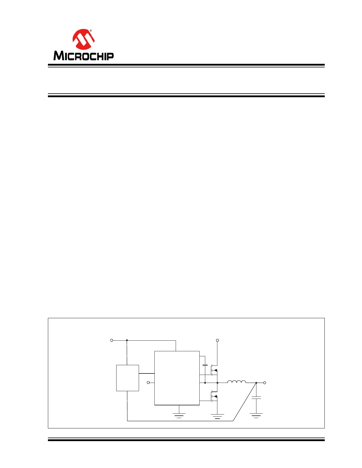
Typical Application Schematic
MIC4102
SOIC-8L
HI
MIC4102
PWM
CONTROLLER
LS
HO
HS
LO
HB
VDD
9V TO 16V BIAS
100V SUPPLY
GND
V
OUT
100V Half-Bridge MOSFET Driver
with Anti-Shoot-Through Protection
MIC4102
DS20005575A-page 2
2016 Microchip Technology Inc.
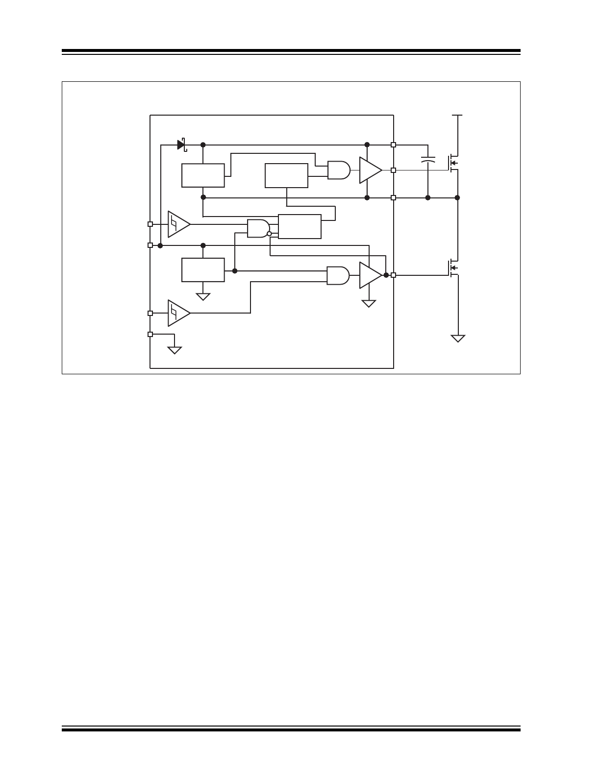
Functional Block Diagram
MIC4102
1
5
6
8
4
3
2
V
SS
DRIVER
UVLO
UVLO
LEVEL
SHIFT
DRIVER
HV
LEVEL
SHIFT
HB
HO
HS
LO
PWM
LS
7
V
DD

2016 Microchip Technology Inc.
DS20005575A-page 3
MIC4102
1.0
ELECTRICAL CHARACTERISTICS
Absolute Maximum Ratings †
Supply Voltage (V
DD
, V
HB
– V
HS
) .............................................................................................................. –0.3V to +18V
Input Voltages (V
PWM
, V
LS
)...............................................................................................................–0.3V to V
DD
+ 0.3V
Voltage on LO (V
LO
)..........................................................................................................................–0.3V to V
DD
+ 0.3V
Voltage on HO (V
HO
).................................................................................................................V
HS
– 0.3V to V
HB
+ 0.3V
Voltage on HS (Continuous).........................................................................................................................–1V to +110V
Voltage on HB ......................................................................................................................................................... +118V
Average Current in V
DD
to HB Diode ....................................................................................................................100 mA
ESD Rating .............................................................................................................................................................
Note 1
Operating Ratings ‡
Supply Voltage (V
DD
) .................................................................................................................................... +9V to +16V
Voltage on HS ............................................................................................................................................. –1V to +100V
Voltage on HS (Repetitive Transient).......................................................................................................... –5V to +105V
HS Slew Rate........................................................................................................................................................ 50 V/ns
Voltage on HB .............................................................................................................................. V
HS
+ 8V to V
HS
+ 16V
and ............................................................................................................................................. V
DD
– 1V to V
DD
+ 100V
†
Notice: Stresses above those listed under “Absolute Maximum Ratings” may cause permanent damage to the device.
This is a stress rating only and functional operation of the device at those or any other conditions above those indicated
in the operational sections of this specification is not intended. Exposure to maximum rating conditions for extended
periods may affect device reliability.
‡ Notice:
The device is not guaranteed to function outside its operating ratings.
Note 1:
Devices are ESD sensitive. Handling precautions are recommended. Human body model, 1.5 kΩ in series
with 100 pF.

MIC4102
DS20005575A-page 4
2016 Microchip Technology Inc.
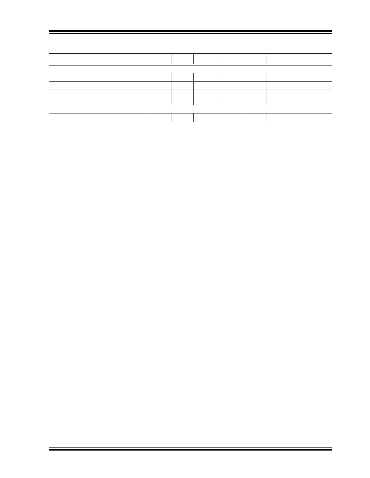
TABLE 1-1:
ELECTRICAL CHARACTERISTICS
Electrical Characteristics:
V
DD
= V
HB
= 12V; V
SS
= V
HS
= 0V; No load on LO or HO; T
A
= +25°C; unless noted.
Bold
values are valid for –40°C ≤ T
J
≤ +125°C. (
Note 1
)
.
Parameters
Sym.
Min.
Typ.
Max.
Units
Conditions
Supply Current
V
DD
Quiescent Current
I
DD
—
150
450
µA
PWM = 0V
—
—
600
V
DD
Operating Current
I
DDO
—
3
3.5
mA
f = 500 kHz
—
—
4.0
Total HB Quiescent Current
I
HB
—
25
150
µA
PWM = 0V
—
—
200
Total HB Operating Current
I
HBO
—
1.5
2.5
mA
f = 500 kHz
—
—
3
HB to V
SS
Quiescent Current
I
HBS
—
0.05
1
µA
V
HS
= V
HB
= 110V
—
—
30
Input Pins (TTL)
Low Level Input Voltage Threshold
V
IL
0.8
1.5
—
V
—
High Level Input Voltage Threshold V
IH
—
1.5
2.2
V
—
Input Pull-Down Resistance
R
I
100
200
500
kΩ
—
Undervoltage Protection
V
DD
Rising Threshold
V
DDR
6.5
7.3
8.0
V
—
V
DD
Threshold Hysteresis
V
DDH
—
0.5
—
V
—
HB Rising Threshold
V
HBR
6.0
7.0
8.0
V
—
HB Threshold Hysteresis
V
HBH
—
0.4
—
V
—
Bootstrap Diode
Low-Current Forward Voltage
V
DL
—
0.4
0.55
V
I
VDD-HB
= 100 µA
—
—
0.70
High-Current Forward Voltage
V
DH
—
0.7
0.8
V
I
VDD-HB
= 100 mA
—
—
1.0
Dynamic Resistance
R
D
—
1.0
1.5
Ω
I
VDD-HB
= 100 mA
—
—
2.0
LO Gate Driver
Low Level Output Voltage
V
OLL
—
0.18
0.3
V
I
LO
= 160 mA
—
—
0.4
High Level Output Voltage
V
OHL
—
0.25
0.3
V
I
LO
= –100 mA,
V
OHL
= V
DD
– V
LO
—
—
0.45
Peak Sink Current
I
OHL
—
3
—
A
V
LO
= 0V
Peak Source Current
I
OLL
—
2
—
A
V
LO
= 12V
Note 1:
Specification for packaged product only.
2:
All voltages relative to Pin 7, V
SS
, unless otherwise specified.
3:
Guaranteed by design. Not production tested.

2016 Microchip Technology Inc.
DS20005575A-page 5
MIC4102
HO Gate Driver
Low Level Output Voltage
V
OLH
—
0.22
0.3
V
I
HO
= 160 mA
—
—
0.4
High Level Output Voltage
V
OHH
—
0.25
0.3
V
I
HO
= –100 mA,
V
OHH
= V
HB
– V
HO
—
—
0.45
Peak Sink Current
I
OHH
—
3
—
A
V
HO
= 0V
Peak Source Current
I
OLH
—
2
—
A
V
HO
= 12V
Switching Specifications (Anti-Shoot-Through Circuitry)
Delay between PWM going high to
LO going low
t
LOOFF
—
30
45
ns
—
—
—
60
Voltage threshold for LO MOSFET
to be considered OFF
V
LOOFF
—
1.7
—
V
—
Delay between LO OFF to HO
going High
t
HOON
—
30
50
ns
—
—
—
60
Delay between PWM going Low to
HO going low
t
HOOFF
—
45
65
ns
—
—
—
70
Switch Node Voltage Threshold
when HO turns off
V
SWth
1
2.5
4
V
—
Delay between HO MOSFET being
considered off to LO turning ON
t
LOON
—
30
60
ns
—
—
—
70
Delay between LS going low and
LO turning OFF
t
LSOFF
—
36
45
ns
C
L
= 1000 pF
—
—
70
Forced LO ON, if V
LOTH
is not
detected
t
SWTO
120
250
450
ns
—
Switching Specifications
Either Output Rise Time (3V to 9V)
t
R
—
10
—
ns
C
L
= 1000 pF
Either Output Fall Time (3V to 9V)
t
F
—
6
—
ns
C
L
= 1000 pF
Either Output Rise Time (3V to 9V)
t
R
—
0.33
0.6
µs
C
L
= 0.1 µF
—
—
0.8
Either Output Fall Time (3V to 9V)
t
F
—
0.2
0.3
µs
C
L
= 0.1 µF
—
—
0.4
Minimum Input Pulse Width that
changes the output with LS = 5V
t
PW
—
40
60
ns
C
L
= 0,
Note 3
Minimum Output Pulse Width on
HO with min pulse width on PWM
with LS = 5V
t
PW
—
15
—
ns
C
L
= 0,
Note 3
TABLE 1-1:
ELECTRICAL CHARACTERISTICS (CONTINUED)
Electrical Characteristics:
V
DD
= V
HB
= 12V; V
SS
= V
HS
= 0V; No load on LO or HO; T
A
= +25°C; unless noted.
Bold
values are valid for –40°C ≤ T
J
≤ +125°C. (
Note 1
)
.
Parameters
Sym.
Min.
Typ.
Max.
Units
Conditions
Note 1:
Specification for packaged product only.
2:
All voltages relative to Pin 7, V
SS
, unless otherwise specified.
3:
Guaranteed by design. Not production tested.

MIC4102
DS20005575A-page 6
2016 Microchip Technology Inc.
Minimum Input Pulse Width that
changes the output with LS = 0V
t
PW
—
13
20
ns
C
L
= 0,
Note 3
Minimum Output Pulse Width on
HO with min pulse width on PWM
with LS = 0V
—
—
20
—
—
C
L
= 0,
Note 3
Bootstrap Diode Turn-On or
Turn-Off Time
t
BS
—
10
—
ns
—
TABLE 1-1:
ELECTRICAL CHARACTERISTICS (CONTINUED)
Electrical Characteristics:
V
DD
= V
HB
= 12V; V
SS
= V
HS
= 0V; No load on LO or HO; T
A
= +25°C; unless noted.
Bold
values are valid for –40°C ≤ T
J
≤ +125°C. (
Note 1
)
.
Parameters
Sym.
Min.
Typ.
Max.
Units
Conditions
Note 1:
Specification for packaged product only.
2:
All voltages relative to Pin 7, V
SS
, unless otherwise specified.
3:
Guaranteed by design. Not production tested.
2016 Microchip Technology Inc.
DS20005575A-page 7
MIC4102
TEMPERATURE SPECIFICATIONS
Parameters
Sym.
Min.
Typ.
Max.
Units
Conditions
Temperature Ranges
Max. Junction Temperature Range
T
J
–55
—
+150
°C
Note 1
Storage Temperature Range
T
S
–60
—
+150
°C
—
Operating Junction Temperature
Range
T
J
–40
—
+125
°C
—
Package Thermal Resistances
Thermal Resistance, SOIC-8L
JA
—
140
—
°C/W
—
Note 1:
The maximum allowable power dissipation is a function of ambient temperature, the maximum allowable
junction temperature and the thermal resistance from junction to air (i.e., T
A
, T
J
,
JA
). Exceeding the
maximum allowable power dissipation will cause the device operating junction temperature to exceed the
maximum +125°C rating. Sustained junction temperatures above +125°C can impact the device reliability.
MIC4102
DS20005575A-page 8
2016 Microchip Technology Inc.
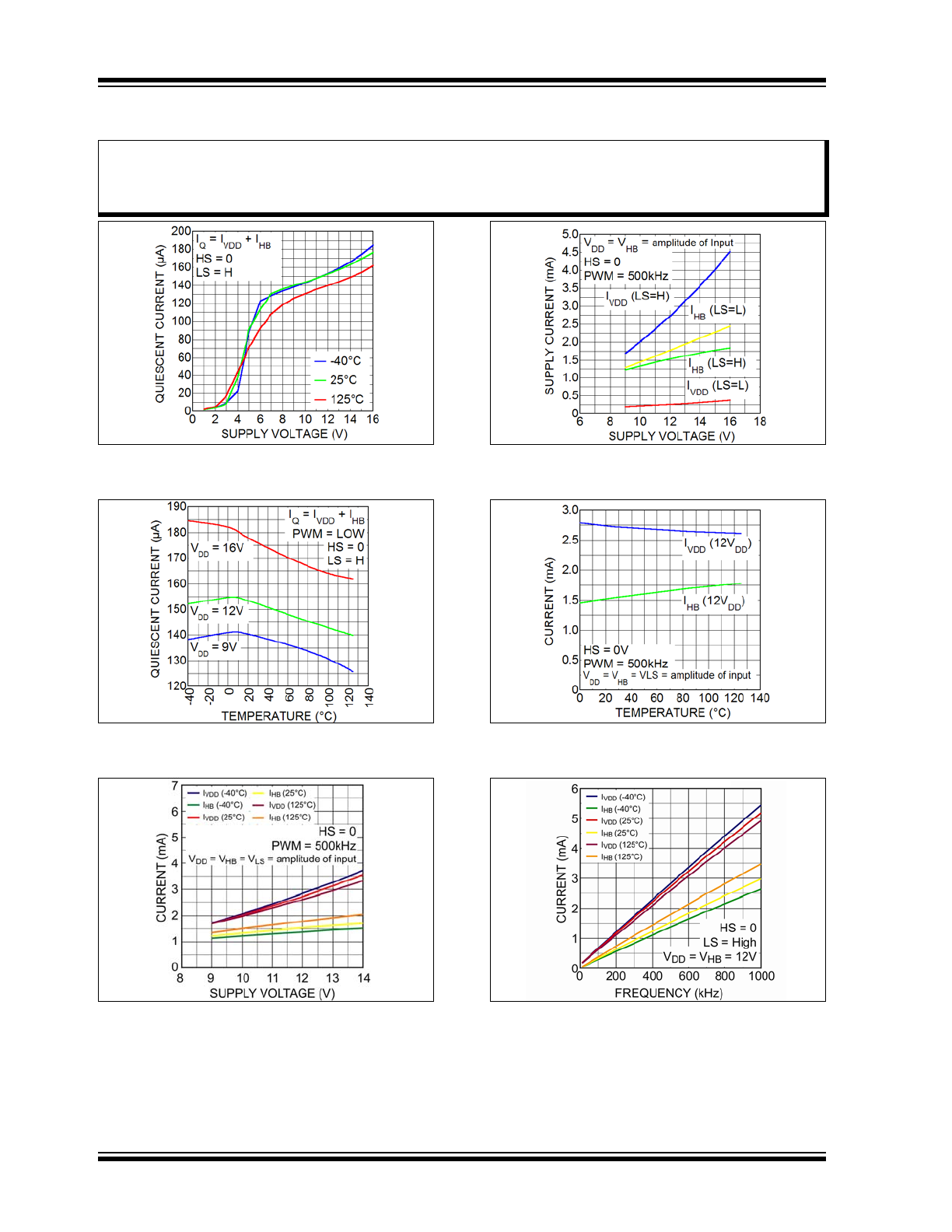
2.0
TYPICAL PERFORMANCE CURVES
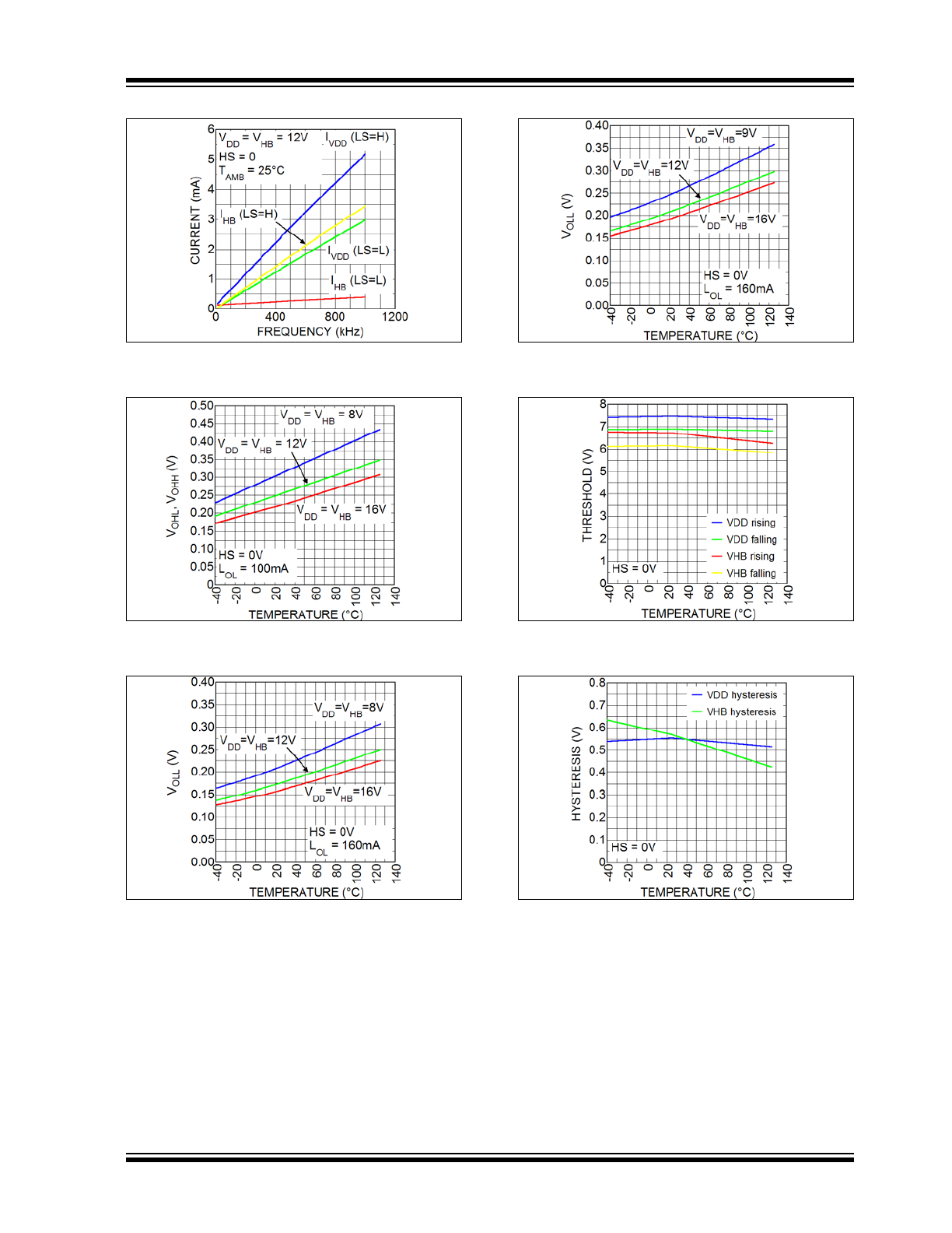
FIGURE 2-1:
Quiescent Current vs.
Supply Voltage.
FIGURE 2-2:
Quiescent Current vs.
Temperature.
FIGURE 2-3:
Operating Current vs.
Supply Voltage.
FIGURE 2-4:
Supply Current vs. Supply
Voltage vs. LS Level.
FIGURE 2-5:
Operating Current vs.
Temperature.
FIGURE 2-6:
Supply Current vs.
Frequency.
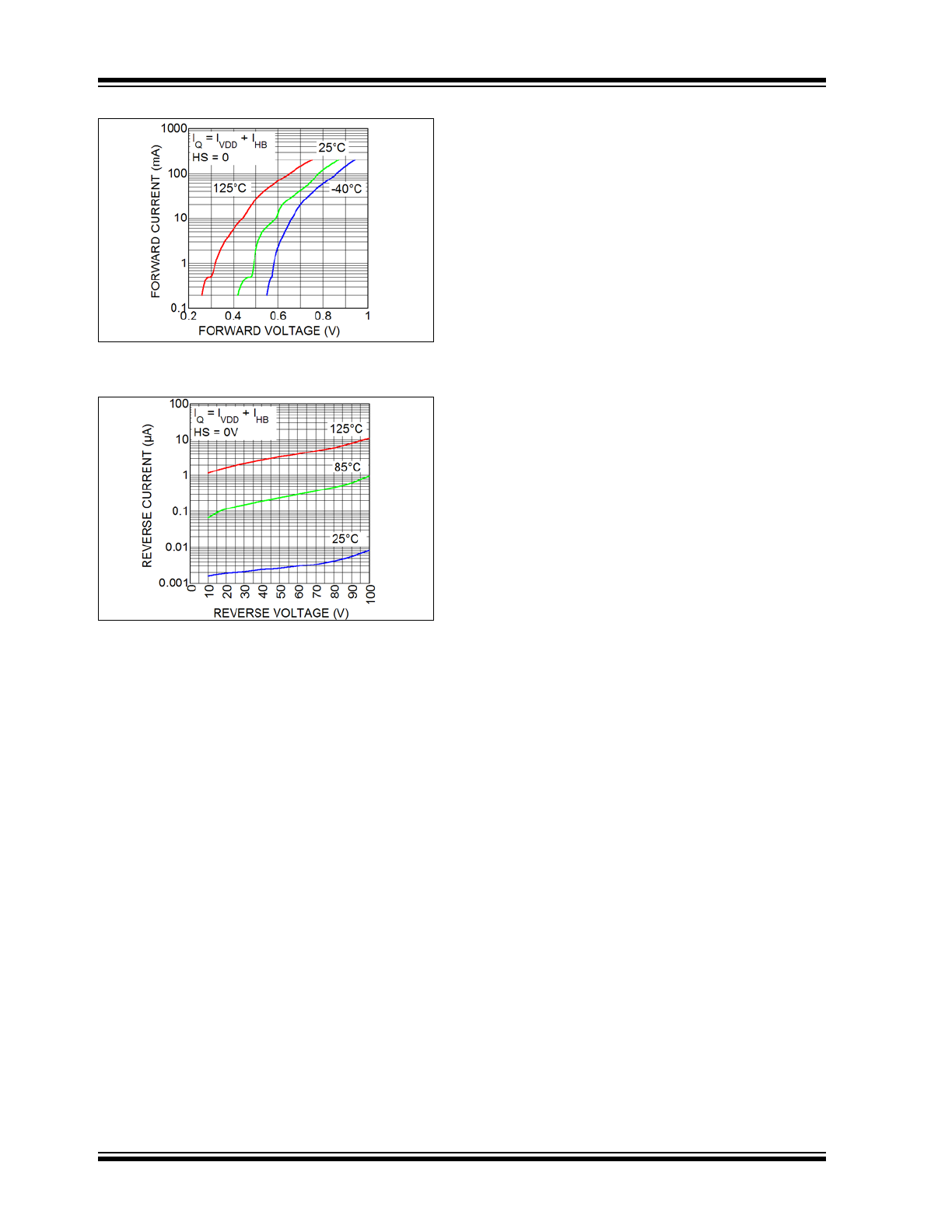
Note:
The graphs and tables provided following this note are a statistical summary based on a limited number of
samples and are provided for informational purposes only. The performance characteristics listed herein
are not tested or guaranteed. In some graphs or tables, the data presented may be outside the specified
operating range (e.g., outside specified power supply range) and therefore outside the warranted range.
2016 Microchip Technology Inc.
DS20005575A-page 9
MIC4102
FIGURE 2-7:
Supply Current vs.
Frequency for Pin L and H.
FIGURE 2-8:
High Level Output Voltage
vs. Temperature.
FIGURE 2-9:
Low Level Output of
Low-Side Driver vs. Temperature.
FIGURE 2-10:
Low Level Output of
Low-Side Driver vs. Temperature.
FIGURE 2-11:
UVLO Thresholds vs.
Temperature.
FIGURE 2-12:
UVLO Hysteresis vs.
Temperature.
MIC4102
DS20005575A-page 10
2016 Microchip Technology Inc.
FIGURE 2-13:
Bootstrap Diode I-V
Characteristics.
FIGURE 2-14:
Bootstrap Diode Reverse
Current.