
© 2009 Microchip Technology Inc.
DS21733J-page 1
MCP6001/1R/1U/2/4
Features
• Available in SC-70-5 and SOT-23-5 packages
• Gain Bandwidth Product: 1 MHz (typical)
• Rail-to-Rail Input/Output
• Supply Voltage: 1.8V to 6.0V
• Supply Current: I
Q
= 100 µA (typical)
• Phase Margin: 90° (typical)
• Temperature Range:
- Industrial: -40°C to +85°C
- Extended: -40°C to +125°C
• Available in Single, Dual and Quad Packages
Applications
• Automotive
• Portable Equipment
• Photodiode Amplifier
• Analog Filters
• Notebooks and PDAs
• Battery-Powered Systems
Design Aids
• SPICE Macro Models
• FilterLab
®
Software
• Mindi™ Circuit Designer & Simulator
• Microchip Advanced Part Selector (MAPS)
• Analog Demonstration and Evaluation Boards
• Application Notes
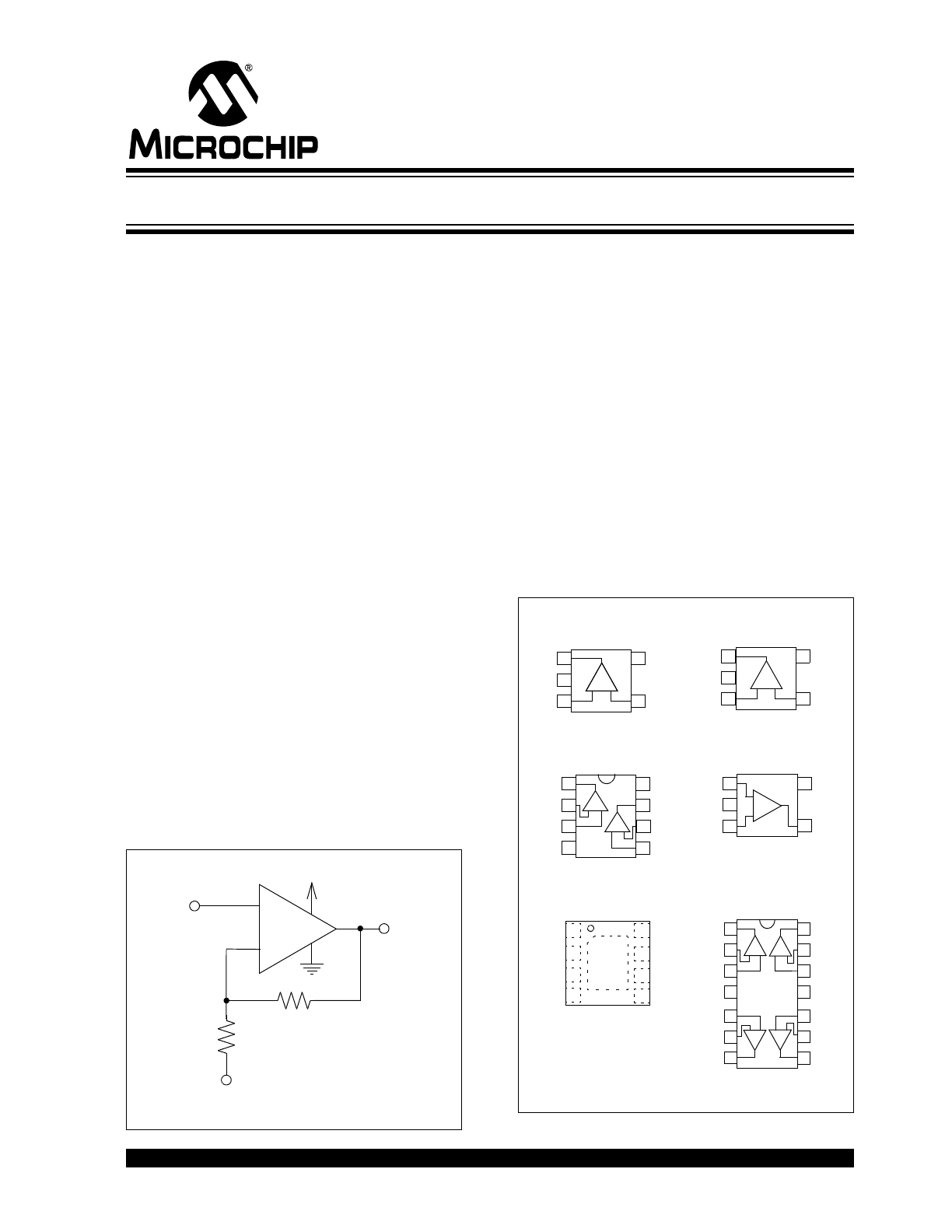
Typical Application
Description
The Microchip Technology Inc. MCP6001/2/4 family of
operational amplifiers (op amps) is specifically
designed for general-purpose applications. This family
has a 1 MHz Gain Bandwidth Product (GBWP) and 90°
phase margin (typical). It also maintains 45° phase
margin (typical) with a 500 pF capacitive load. This
family operates from a single supply voltage as low as
1.8V, while drawing 100 µA (typical) quiescent current.
Additionally, the MCP6001/2/4 supports rail-to-rail input
and output swing, with a common mode input voltage
range of V
DD
+ 300 mV to V
SS
– 300 mV. This family of
op amps is designed with Microchip’s advanced CMOS
process.
The MCP6001/2/4 family is available in the industrial
and extended temperature ranges, with a power supply
range of 1.8V to 6.0V.
Package Types
R
1
V
OUT
R
2
V
IN
V
DD
+
–
Gain
1
R
1
R
2
------
+
=
Non-Inverting Amplifier
MCP6001
V
REF
V
SS
4
5
4
5
4
MCP6001
1
2
3
-
+
5 V
DD
V
IN
–
V
OUT
V
SS
V
IN
+
SC70-5, SOT-23-5
MCP6002
PDIP, SOIC, MSOP
MCP6004
V
INA
+
V
INA
–
V
SS
1
2
3
4
14
13
12
11
-
V
OUTA
+ -
+
V
DD
V
OUTD
V
IND
–
V
IND
+
10
9
8
5
6
7
V
OUTB
V
INB
–
V
INB
+
V
INC
+
V
INC
–
V
OUTC
+
-
-
+
PDIP, SOIC, TSSOP
V
INA
+
V
INA
–
V
SS
1
2
3
4
8
7
6
5
-
V
OUTA
+
-
+
V
DD
V
OUTB
V
INB
–
V
INB
+
4
1
2
3
-
+
5 V
DD
V
OUT
V
SS
MCP6001R
SOT-23-5
1
2
3
-
+
V
SS
V
IN
–
V
OUT
V
DD
V
IN
+
MCP6001U
SOT-23-5
1
2
3
-
+
V
DD
V
OUT
V
IN
+
V
SS
V
IN
–
MCP6002
V
INA
+
V
INA
–
V
SS
V
OUTB
V
INB
–
1
2
3
4
8
7
6
5
V
INB
+
V
OUTA
EP
9
V
DD
2x3 DFN *
* Includes Exposed Thermal Pad (EP); see
Table 3-1
.
1 MHz, Low-Power Op Amp

MCP6001/1R/1U/2/4
DS21733J-page 2
© 2009 Microchip Technology Inc.
NOTES:
© 2009 Microchip Technology Inc.
DS21733J-page 3
MCP6001/1R/1U/2/4
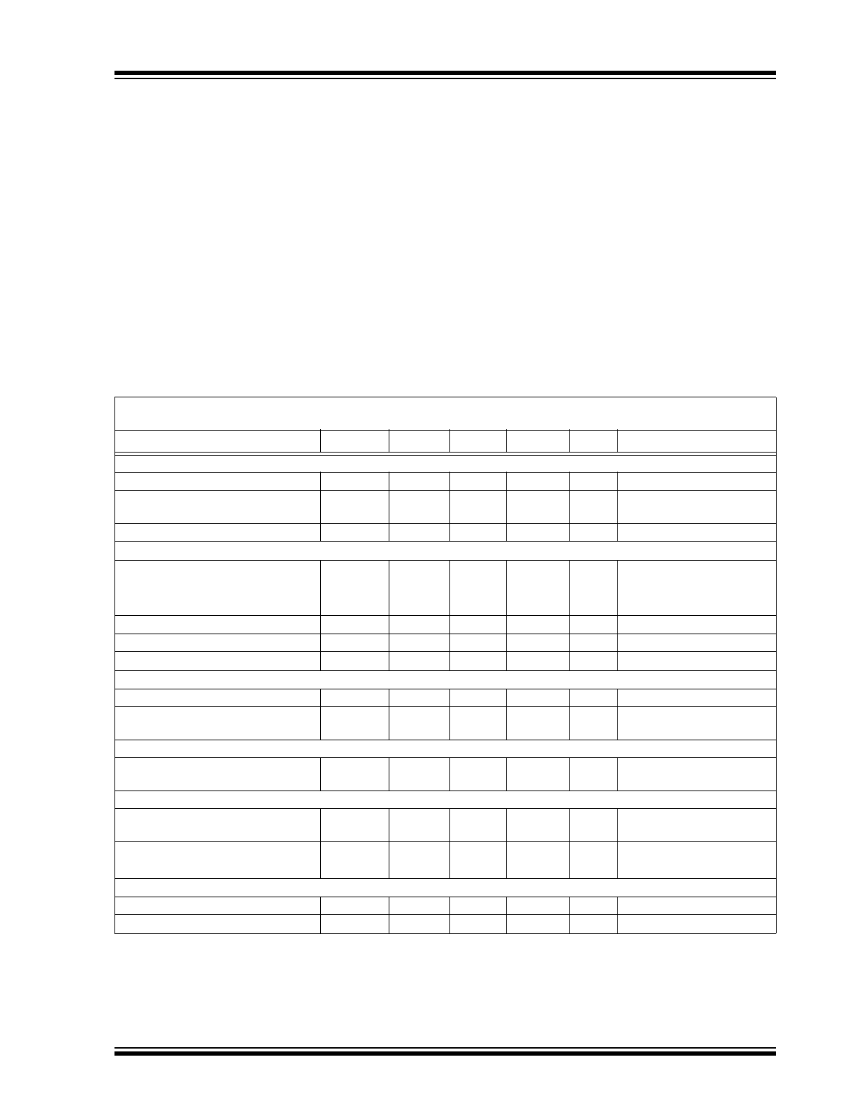
1.0
ELECTRICAL
CHARACTERISTICS
Absolute Maximum Ratings †
V
DD
– V
SS
........................................................................7.0V
Current at Analog Input Pins (V
IN
+, V
IN
–) .....................±2 mA
Analog Inputs (V
IN
+, V
IN
–) †† ........ V
SS
– 1.0V to V
DD
+ 1.0V
All Other Inputs and Outputs ......... V
SS
– 0.3V to V
DD
+ 0.3V
Difference Input Voltage ...................................... |V
DD
– V
SS
|
Output Short Circuit Current ................................ Continuous
Current at Output and Supply Pins ............................±30 mA
Storage Temperature ................................... –65°C to +150°C
Maximum Junction Temperature (T
J
) ......................... .+150°C
ESD Protection On All Pins (HBM; MM)
.............. ≥ 4 kV; 200V
† Notice: Stresses above those listed under “Absolute
Maximum Ratings” may cause permanent damage to the
device. This is a stress rating only and functional operation of
the device at those or any other conditions above those
indicated in the operational listings of this specification is not
implied. Exposure to maximum rating conditions for extended
periods may affect device reliability.
†† See Section 4.1.2 “Input Voltage and Current Limits”.
DC ELECTRICAL SPECIFICATIONS
Electrical Characteristics: Unless otherwise indicated, T
A
= +25°C, V
DD
= +1.8V to +5.5V, V
SS
= GND, V
CM
= V
DD
/2, V
L
= V
DD
/2,
R
L
= 10 k
Ω to V
L
, and V
OUT
≈ V
DD
/2 (refer to
Figure 1-1
).
Parameters
Sym
Min
Typ
Max
Units
Conditions
Input Offset
Input Offset Voltage
V
OS
-4.5
—
+4.5
mV
V
CM
= V
SS
(Note 1)
Input Offset Drift with Temperature
ΔV
OS
/
ΔT
A
—
±2.0
—
µV/°C
T
A
= -40°C to +125°C,
V
CM
= V
SS
Power Supply Rejection Ratio
PSRR
—
86
—
dB
V
CM
= V
SS
Input Bias Current and Impedance
Input Bias Current:
I
B
—
±1.0
—
pA
Industrial Temperature
I
B
—
19
—
pA
T
A
= +85°C
Extended Temperature
I
B
—
1100
—
pA
T
A
= +125°C
Input Offset Current
I
OS
—
±1.0
—
pA
Common Mode Input Impedance
Z
CM
—
10
13
||6
—
Ω||pF
Differential Input Impedance
Z
DIFF
—
10
13
||3
—
Ω||pF
Common Mode
Common Mode Input Range
V
CMR
V
SS
− 0.3
—
V
DD
+ 0.3
V
Common Mode Rejection Ratio
CMRR
60
76
—
dB
V
CM
= -0.3V to 5.3V,
V
DD
= 5V
Open-Loop Gain
DC Open-Loop Gain (Large Signal)
A
OL
88
112
—
dB
V
OUT
= 0.3V to V
DD
– 0.3V,
V
CM
= V
SS
Output
Maximum Output Voltage Swing
V
OL
, V
OH
V
SS
+
25
—
V
DD
– 25
mV
V
DD
= 5.5V,
0.5V Input Overdrive
Output Short Circuit Current
I
SC
—
±6
—
mA
V
DD
= 1.8V
—
±23
—
mA
V
DD
= 5.5V
Power Supply
Supply Voltage
V
DD
1.8
—
6.0
V
Note 2
Quiescent Current per Amplifier
I
Q
50
100
170
µA
I
O
= 0, V
DD
= 5.5V, V
CM
= 5V
Note 1:
MCP6001/1R/1U/2/4 parts with date codes prior to December 2004 (week code 49) were tested to ±7 mV minimum/
maximum limits.
2:
All parts with date codes November 2007 and later have been screened to ensure operation at
V
DD
= 6.0V. However, the other minimum and maximum specifications are measured at 1.8V and 5.5V.
MCP6001/1R/1U/2/4
DS21733J-page 4
© 2009 Microchip Technology Inc.
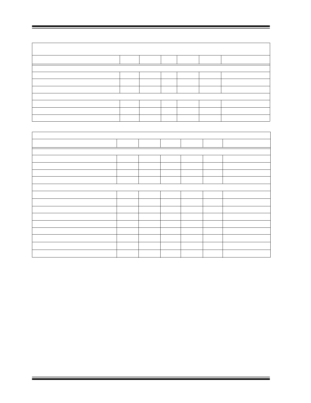
AC ELECTRICAL SPECIFICATIONS
TEMPERATURE SPECIFICATIONS
Electrical Characteristics: Unless otherwise indicated, T
A
= +25°C, V
DD
= +1.8 to 5.5V, V
SS
= GND, V
CM
= V
DD
/2,
V
L
= V
DD
/2, V
OUT
≈ V
DD
/2, R
L
= 10 k
Ω to V
L
, and C
L
= 60 pF (refer to
Figure 1-1
).
Parameters
Sym
Min
Typ
Max
Units
Conditions
AC Response
Gain Bandwidth Product
GBWP
—
1.0
—
MHz
Phase Margin
PM
—
90
—
°
G = +1 V/V
Slew Rate
SR
—
0.6
—
V/µs
Noise
Input Noise Voltage
E
ni
—
6.1
—
µVp-p
f = 0.1 Hz to 10 Hz
Input Noise Voltage Density
e
ni
—
28
—
nV/
√Hz f = 1 kHz
Input Noise Current Density
i
ni
—
0.6
—
fA/
√Hz f = 1 kHz
Electrical Characteristics: Unless otherwise indicated, V
DD
= +1.8V to +5.5V and V
SS
= GND.
Parameters
Sym
Min
Typ
Max
Units
Conditions
Temperature Ranges
Industrial Temperature Range
T
A
-40
—
+85
°C
Extended Temperature Range
T
A
-40
—
+125
°C
Operating Temperature Range
T
A
-40
—
+125
°C
Note
Storage Temperature Range
T
A
-65
—
+150
°C
Thermal Package Resistances
Thermal Resistance, 5L-SC70
θ
JA
—
331
—
°C/W
Thermal Resistance, 5L-SOT-23
θ
JA
—
256
—
°C/W
Thermal Resistance, 8L-PDIP
θ
JA
—
85
—
°C/W
Thermal Resistance, 8L-SOIC (150 mil)
θ
JA
—
163
—
°C/W
Thermal Resistance, 8L-MSOP
θ
JA
—
206
—
°C/W
Thermal Resistance, 8L-DFN (2x3)
θ
JA
—
68
—
°C/W
Thermal Resistance, 14L-PDIP
θ
JA
—
70
—
°C/W
Thermal Resistance, 14L-SOIC
θ
JA
—
120
—
°C/W
Thermal Resistance, 14L-TSSOP
θ
JA
—
100
—
°C/W
Note:
The industrial temperature devices operate over this extended temperature range, but with reduced
performance. In any case, the internal Junction Temperature (T
J
) must not exceed the Absolute Maximum
specification of +150°C.
© 2009 Microchip Technology Inc.
DS21733J-page 5
MCP6001/1R/1U/2/4
1.1
Test Circuits
The circuit used for most DC and AC tests is shown in
Figure 1-1
. This circuit can independently set V
CM
and
V
OUT
; see
Equation 1-1
. Note that V
CM
is not the
circuit’s common mode voltage ((V
P
+ V
M
)/2), and that
V
OST
includes V
OS
plus the effects (on the input offset
error, V
OST
) of temperature, CMRR, PSRR and A
OL
.
EQUATION 1-1:
FIGURE 1-1:
AC and DC Test Circuit for
Most Specifications.
G
DM
R
F
R
G
⁄
=
V
CM
V
P
V
DD
2
⁄
+
(
) 2
⁄
=
V
OUT
V
DD
2
⁄
(
)
V
P
V
M
–
(
) V
OST
1
G
DM
+
(
)
+
+
=
Where:
G
DM
= Differential Mode Gain
(V/V)
V
CM
= Op Amp’s Common Mode
Input Voltage
(V)
V
OST
= Op Amp’s Total Input Offset
Voltage
(mV)
V
OST
V
IN–
V
IN+
–
=
V
DD
R
G
R
F
V
OUT
V
M
C
B2
C
L
R
L
V
L
C
B1
100 k
Ω
100 k
Ω
R
G
R
F
V
DD
/2
V
P
100 k
Ω
100 k
Ω
60 pF
10 k
Ω
1 µF
100 nF
V
IN–
V
IN+
C
F
6.8 pF
C
F
6.8 pF
MCP600X

MCP6001/1R/1U/2/4
DS21733J-page 6
© 2009 Microchip Technology Inc.
NOTES:
© 2009 Microchip Technology Inc.
DS21733J-page 7
MCP6001/1R/1U/2/4
2.0
TYPICAL PERFORMANCE CURVES
Note: Unless otherwise indicated, T
A
= +25°C, V
DD
= +1.8V to +5.5V, V
SS
= GND, V
CM
= V
DD
/2, V
OUT
≈ V
DD
/2,
V
L
= V
DD
/2, R
L
= 10 k
Ω to V
L
, and C
L
= 60 pF.
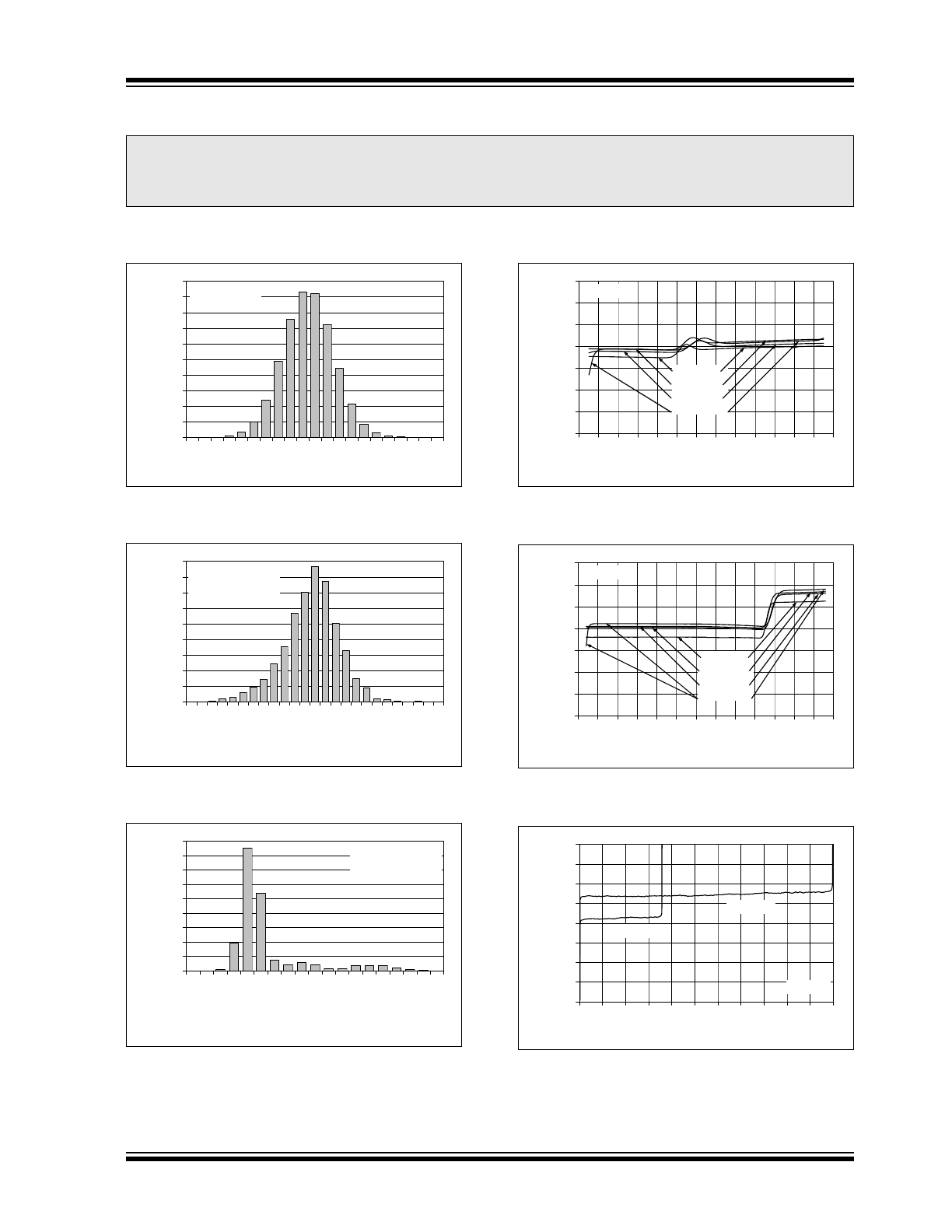
FIGURE 2-1:
Input Offset Voltage.
FIGURE 2-2:
Input Offset Voltage Drift.
FIGURE 2-3:
Input Offset Quadratic
Temp. Co.
FIGURE 2-4:
Input Offset Voltage vs.
Common Mode Input Voltage at V
DD
= 1.8V.
FIGURE 2-5:
Input Offset Voltage vs.
Common Mode Input Voltage at V
DD
= 5.5V.
FIGURE 2-6:
Input Offset Voltage vs.
Output Voltage.
Note:
The graphs and tables provided following this note are a statistical summary based on a limited number of
samples and are provided for informational purposes only. The performance characteristics listed herein
are not tested or guaranteed. In some graphs or tables, the data presented may be outside the specified
operating range (e.g., outside specified power supply range) and therefore outside the warranted range.
0%
2%
4%
6%
8%
10%
12%
14%
16%
18%
20%
5
-4
-3
-2
-1
0
1
2
3
4
5
Input Offset Voltage (mV)
Percent
age of
Occurrences
64,695 Samples
V
CM
= V
SS
0%
2%
4%
6%
8%
10%
12%
14%
16%
18%
-12 -10 -8 -6 -4 -2
0
2
4
6
8 10 12
Input Offset Voltage Drift;
TC
1
(µV/°C)
Percent
age of Occurrences
2453 Samples
T
A
= -40°C to +125°C
V
CM
= V
SS
0%
5%
10%
15%
20%
25%
30%
35%
40%
45%
-0
.02
-0
.01
0.
0
0
0.
0
1
0.
0
2
0.
0
3
0.
0
4
0.
0
5
0.
0
6
0.
0
7
Input Offset Quadratic Temp. Co.;
TC
2
(µV/°C
2
)
Percent
age of Occurrences
2453 Samples
T
A
= -40°C to +125°C
V
CM
= V
SS
-700
-600
-500
-400
-300
-200
-100
0
-0
.4
-0
.2
0.
0
0.
2
0.
4
0.
6
0.
8
1.
0
1.
2
1.
4
1.
6
1.
8
2.
0
2.
2
Common Mode Input Voltage (V)
Input
Off
set Voltage (
µ
V)
V
DD
= 1.8V
T
A
= -40°C
T
A
= +25°C
T
A
= +85°C
T
A
= +125°C
-700
-600
-500
-400
-300
-200
-100
0
-0
.5
0.
0
0.
5
1.
0
1.
5
2.
0
2.
5
3.
0
3.
5
4.
0
4.
5
5.
0
5.
5
6.
0
Common Mode Input Voltage (V)
Input Of
fset
V
o
lt
age (µV
)
V
DD
= 5.5V
T
A
= -40°C
T
A
= +25°C
T
A
= +85°C
T
A
= +125°C
-200
-150
-100
-50
0
50
100
150
200
0.0 0.5 1.0 1.5 2.0 2.5 3.0 3.5 4.0 4.5 5.0 5.5
Output Voltage (V)
Input
Off
s
et
V
o
lt
age (µV
)
V
DD
= 1.8V
V
CM
= V
SS
V
DD
= 5.5V
MCP6001/1R/1U/2/4
DS21733J-page 8
© 2009 Microchip Technology Inc.
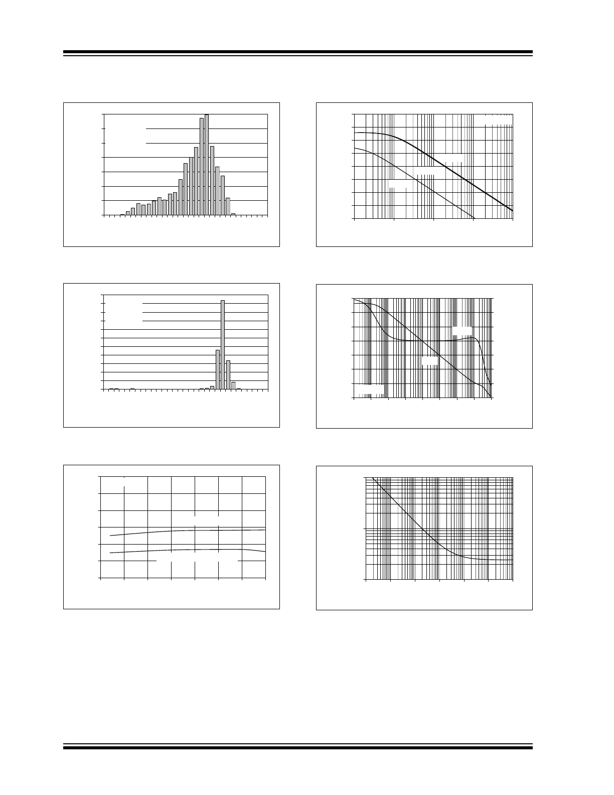
Note: Unless otherwise indicated, T
A
= +25°C, V
DD
= +1.8V to +5.5V, V
SS
= GND, V
CM
= V
DD
/2, V
OUT
≈ V
DD
/2,
V
L
= V
DD
/2, R
L
= 10 k
Ω to V
L
, and C
L
= 60 pF.
FIGURE 2-7:
Input Bias Current at +85°C.
FIGURE 2-8:
Input Bias Current at
+125°C.
FIGURE 2-9:
CMRR, PSRR vs. Ambient
Temperature.
FIGURE 2-10:
PSRR, CMRR vs.
Frequency.
FIGURE 2-11:
Open-Loop Gain, Phase vs.
Frequency.
FIGURE 2-12:
Input Noise Voltage Density
vs. Frequency.
0%
2%
4%
6%
8%
10%
12%
14%
0
3
6
9
12
15
18 21 24 27
30
Input Bias Current (pA)
Percent
age of
Occurrences
1230 Samples
V
DD
= 5.5V
V
CM
= V
DD
T
A
= +85°C
0%
5%
10%
15%
20%
25%
30%
35%
40%
45%
50%
55%
0
15
0
30
0
45
0
60
0
75
0
90
0
10
50
12
00
13
50
15
00
Input Bias Current (pA)
Percent
age of Occurrences
605 Samples
V
DD
= 5.5V
V
CM
= V
DD
T
A
= +125°C
70
75
80
85
90
95
100
-50
-25
0
25
50
75
100
125
Ambient Temperature (°C)
PSRR, CMRR (
d
B)
PSRR (V
CM
= V
SS
)
CMRR (V
CM
= -0.3V to +5.3V)
V
DD
= 5.0V
20
30
40
50
60
70
80
90
100
1.E+01
1.E+02
1.E+03
1.E+04
1.E+05
Frequency (Hz)
PSRR, CM
RR (dB)
PSRR+
CMRR
PSRR–
V
CM
= V
SS
10
100
1k
10k
100k
-20
0
20
40
60
80
100
120
1.E-
01
1.E+
00
1.E+
01
1.E+
02
1.E+
03
1.E+
04
1.E+
05
1.E+
06
1.E+
07
Frequency (Hz)
Open-Loop Gain (dB)
-210
-180
-150
-120
-90
-60
-30
0
Open-
Loop P
h
ase (
°)
0.1
1
10 100
10k 100k 1M 10M
Phase
Gain
1k
V
CM
= V
SS
10
100
1,000
1.E-01 1.E+0
0
1.E+0
1
1.E+0
2
1.E+0
3
1.E+0
4
1.E+0
5
Frequency (Hz)
Input Noise Voltage Density
(n
V
/√
Hz)
0.1
10
1
100
10k
1k
100k
© 2009 Microchip Technology Inc.
DS21733J-page 9
MCP6001/1R/1U/2/4
Note: Unless otherwise indicated, T
A
= +25°C, V
DD
= +1.8V to +5.5V, V
SS
= GND, V
CM
= V
DD
/2, V
OUT
≈ V
DD
/2,
V
L
= V
DD
/2, R
L
= 10 k
Ω to V
L
, and C
L
= 60 pF.
FIGURE 2-13:
Output Short Circuit Current
vs. Power Supply Voltage.
FIGURE 2-14:
Output Voltage Headroom
vs. Output Current Magnitude.
FIGURE 2-15:
Quiescent Current vs.
Power Supply Voltage.
FIGURE 2-16:
Small-Signal, Non-Inverting
Pulse Response.
FIGURE 2-17:
Large-Signal, Non-Inverting
Pulse Response.
FIGURE 2-18:
Slew Rate vs. Ambient
Temperature.
0
5
10
15
20
25
30
0.0 0.5 1.0 1.5 2.0 2.5 3.0 3.5 4.0 4.5 5.0 5.5
Power Supply Voltage (V)
S
hort Circuit Current
Magn
it
ude (
m
A)
T
A
= -40°C
T
A
= +25°C
T
A
= +85°C
T
A
= +125°C
1
10
100
1,000
1.E-05
1.E-04
1.E-03
1.E-02
Output Current Magnitude (A)
Output
V
o
lt
age Head
room
(mV
)
V
DD
– V
OH
10µ
10m
1m
100µ
V
OL
– V
SS
0
20
40
60
80
100
120
140
160
180
0.0 0.5 1.0 1.5 2.0 2.5 3.0 3.5 4.0 4.5 5.0 5.5
Power Supply Voltage (V)
Q
u
ie
sc
ent Cur
re
nt
pe
r amplifier (µA)
V
CM
= V
DD
- 0.5V
T
A
= +125°C
T
A
= +85°C
T
A
= +25°C
T
A
= -40°C
-0.08
-0.06
-0.04
-0.02
0.00
0.02
0.04
0.06
0.08
0.E+00
1.E-06
2.E-06
3.E-06
4.E-06
5.E-06
6.E-06
7.E-06
8.E-06
9.E-06
1.E-05
Time (1 µs/div)
Output Voltage
(2
0 mV
/d
iv
)
G = +1 V/V
0.0
0.5
1.0
1.5
2.0
2.5
3.0
3.5
4.0
4.5
5.0
0.E+00
1.E-05
2.E-05
3.E-05
4.E-05
5.E-05
6.E-05
7.E-05
8.E-05
9.E-05
1.E-04
Time (10 µs/div)
Out
put Voltage (
V
)
G = +1 V/V
V
DD
= 5.0V
0.0
0.1
0.2
0.3
0.4
0.5
0.6
0.7
0.8
0.9
1.0
-50
-25
0
25
50
75
100
125
Ambient Temperature (°C)
S
lew Ra
te
(V
/µ
s
)
V
DD
= 5.5V
V
DD
= 1.8V
Rising Edge
Falling Edge
MCP6001/1R/1U/2/4
DS21733J-page 10
© 2009 Microchip Technology Inc.
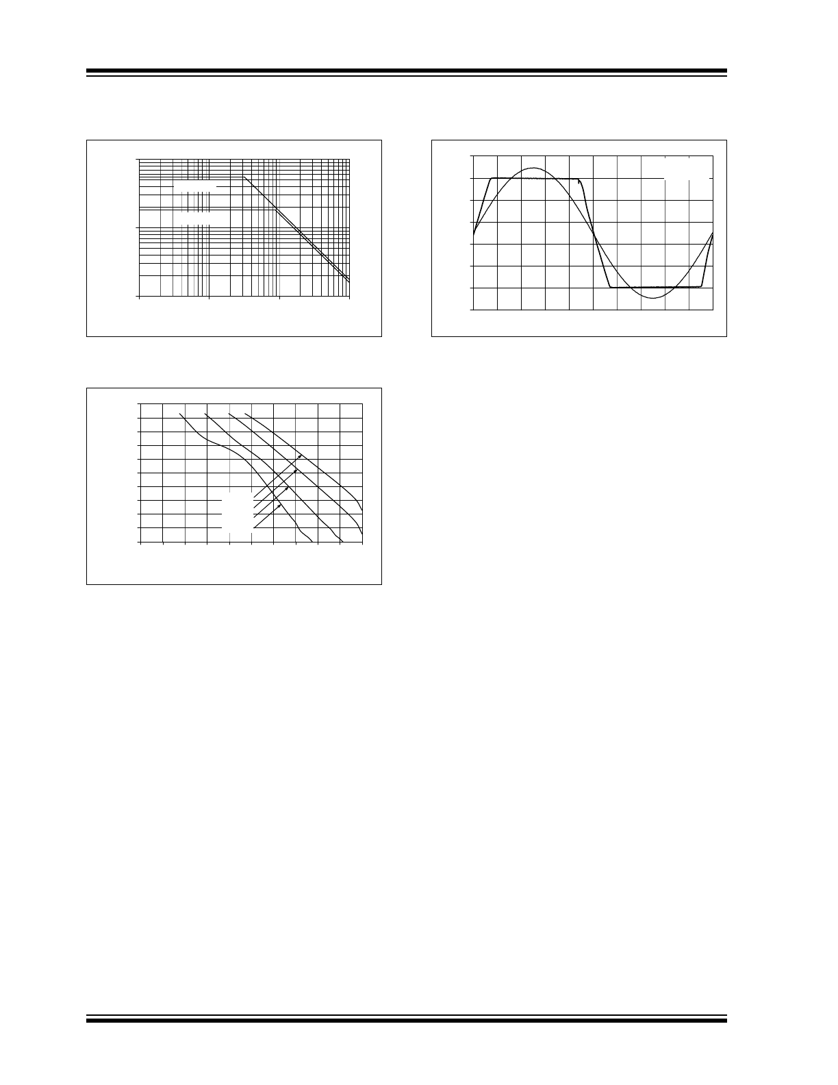
Note: Unless otherwise indicated, T
A
= +25°C, V
DD
= +1.8V to +5.5V, V
SS
= GND, V
CM
= V
DD
/2, V
OUT
≈ V
DD
/2,
V
L
= V
DD
/2, R
L
= 10 k
Ω to V
L
, and C
L
= 60 pF.
FIGURE 2-19:
Output Voltage Swing vs.
Frequency.
FIGURE 2-20:
Measured Input Current vs.
Input Voltage (below V
SS
).
FIGURE 2-21:
The MCP6001/2/4 Show No
Phase Reversal.
0.1
1
10
1.E+03
1.E+04
1.E+05
1.E+06
Frequency (Hz)
Output Voltage
Swing (V
P-P
)
V
DD
= 5.5V
1k
10k
100k
1M
V
DD
= 1.8V
1.E-12
1.E-11
1.E-10
1.E-09
1.E-08
1.E-07
1.E-06
1.E-05
1.E-04
1.E-03
1.E-02
-1.0 -0.9 -0.8 -0.7 -0.6 -0.5 -0.4 -0.3 -0.2 -0.1 0.0
Input Voltage (V)
Input
C
u
rrent M
agnit
ude (
A
)
+125°C
+85°C
+25°C
-40°C
10m
1m
100µ
10µ
1µ
100n
10n
1n
100p
10p
1p
-1
0
1
2
3
4
5
6
0.E+00
1.E-05
2.E-05
3.E-05
4.E-05
5.E-05
6.E-05
7.E-05
8.E-05
9.E-05
1.E-04
Time (10 µs/div)
Input, Out
put Voltages (V)
V
DD
= 5.0V
G = +2 V/V
V
IN
V
OUT