
2016 Microchip Technology Inc.
DS20005616A-page 1
PL610-01/-02/-03
Features
• Single Die, Wide Frequency Coverage,
Programmable Advanced Oscillator Design
• Single IC to Cover up to 130 MHz Output
Frequency.
• Direct Oscillation Operation with Optional
Programmable Features:
- ±50 ppm Frequency Tuning
- Output Drive Setting (4 mA, 8 mA, or 16 mA)
- 6-Bit Odd/Even Output Divider (≤ ÷63)
• Fundamental Crystal Input Frequency:
- 10 MHz to 60 MHz (Default)
- 60 MHz to 130 MHz (Programming Option)
• Output Frequency: LVCMOS
- 80 kHz to 130 MHz
• Wire Bond and Flip Chip Options to Choose from
• Very Low Jitter and Phase Noise
• Low Current Consumption
• Single 1.8V, 2.5V, or 3.3V ±10% Power Supply
• Operating Temperature Range from –40°C to
+85°C
General Description
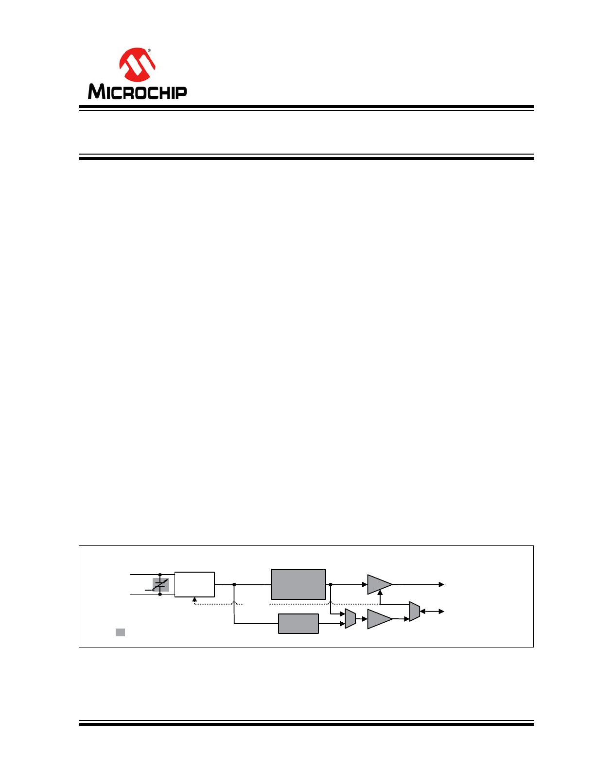
The PL610 is a high performance general purpose
clock that uses a single die to cover outputs up to
130 MHz, eliminating the need for multiple ICs to cover
a wide frequency range. Designed to fit in a small
2.0 mm x 1.6 mm, or larger substrates, the PL610
offers the best phase noise and jitter performance,
smallest die size, and lowest power consumption of
any comparable IC.
The optional ‘frequency fine tuning’ feature of PL610
allows for frequency adjustment after encapsulation of
the module, up to ±50 ppm. In addition, there is a ‘6’ bit
optional programmable Odd/Even divider (default =
÷1), and three programmable output drive strengths
(4 mA, 8 mA (default), 16 mA) to choose from. The full
feature set of PL610 makes it the most versatile XO for
any application.
Block Diagram
PL610-01/-02/-03
FIN
XOUT
CLK0
OE, PDB, CLK1
Programmable
C
LOAD
Programmable Function
/1,2
XTAL
OSC
P-Counter
(6-bit)
(PDB)
F
REF
1.8V to 3.3V Single IC XO
with Frequency Tuning (10 MHz to 130 MHz)

PL610-01/-02/-03
DS20005616A-page 2
2016 Microchip Technology Inc.
1.0
ELECTRICAL CHARACTERISTICS
Absolute Maximum Ratings †
Supply Voltage (V
DD
) ................................................................................................................................ –0.5V to +7.0V
Input Voltage (V
IN
).............................................................................................................................–0.5V to V
DD
+ 0.5V
Output Voltage (V
OUT
).......................................................................................................................–0.5V to V
DD
+ 0.5V
†
Notice: Stresses above those listed under “Absolute Maximum Ratings” may cause permanent damage to the device.
This is a stress rating only and functional operation of the device at those or any other conditions above those indicated
in the operational sections of this specification is not intended. Exposure to maximum rating conditions for extended
periods may affect device reliability. Parts are tested to commercial grade only.
2016 Microchip Technology Inc.
DS20005616A-page 3
PL610-01/-02/-03
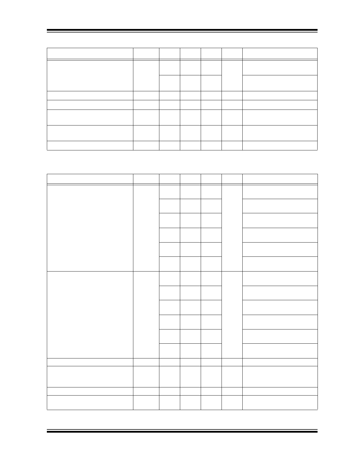
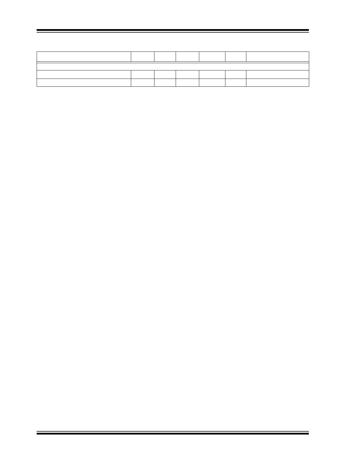
TABLE 1-1:
AC ELECTRICAL CHARACTERISTICS
Parameters
Sym.
Min.
Typ.
Max.
Units
Conditions
Crystal Input Frequency (XIN)
—
10
—
60
MHz
Fundamental Crystal,
Low Frequency
60
—
130
Fundamental Crystal,
High Frequency
Output Frequency
—
.080
—
130
MHz
@ V
DD
= 1.8V to 3.3V, ±10%
V
DD
Sensitivity
—
–2
—
+2
ppm
Frequency vs. V
DD
±10%
Output Rise Time (see
Figure 3-1
)
—
—
1
1.2
ns
15 pF Load, 10/90% V
DD
,
High Drive, 3.3V
Output Fall Time (see
Figure 3-1
)
—
—
1
1.2
ns
15 pF Load, 10/90% V
DD
,
High Drive, 3.3V
Duty Cycle (
Note 1
, see
Figure 3-1
)
—
45
50
55
%
—
Note 1:
For 1.8V operation, the 50% ±5% duty cycle is guaranteed for frequencies ≤40 MHz.
TABLE 1-2:
DC ELECTRICAL CHARACTERISTICS
Parameters
Sym.
Min.
Typ.
Max.
Units
Conditions
Supply Current, Dynamic, with
Loaded LVCMOS Output
I
DD
—
3.7
—
mA
V
DD
= 3.3V, 40 MHz,
Load = 15 pF
—
2.75
—
V
DD
= 2.5V, 40 MHz,
Load = 15 pF
—
2.0
—
V
DD
= 1.8V, 40 MHz,
Load = 15 pF
—
2.5
—
V
DD
= 3.3V, 26 MHz,
Load = 15 pF
—
1.8
—
V
DD
= 2.5V, 26 MHz,
Load = 15 pF
—
1.3
—
V
DD
= 1.8V, 26 MHz,
Load = 15 pF
Supply Current, Dynamic, with
Unloaded LVCMOS Output
—
—
1.65
—
mA
V
DD
= 3.3V, 40 MHz,
No Load
—
1.2
—
V
DD
= 2.5V, 40 MHz,
No Load
—
0.9
—
V
DD
= 1.8V, 40 MHz,
No Load
—
1.2
—
V
DD
= 3.3V, 26 MHz,
No Load
—
0.8
—
V
DD
= 2.5V, 26 MHz,
No Load
—
0.58
—
V
DD
= 1.8V, 26 MHz,
No Load
Operating Voltage
V
DD
1.62
—
3.63
V
—
Power Supply Ramp
t
PU
0.001
—
100
ms
Time for V
DD
to reach 90%
V
DD
. Power ramp must be
monotonic.
Output Low Voltage
V
OL
—
—
0.1
V
I
OL
= +4 mA Standard Drive
Output High Voltage
V
OH
V
DD
–
0.4
—
—
V
I
OH
= –4 mA Standard Drive
PL610-01/-02/-03
DS20005616A-page 4
2016 Microchip Technology Inc.
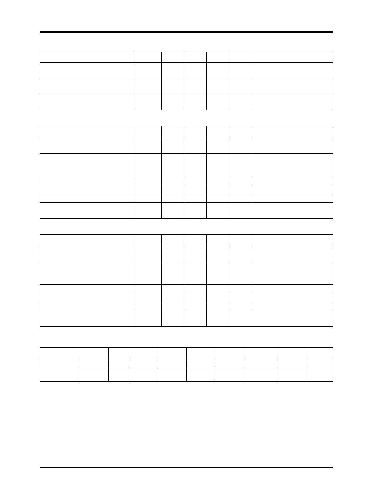
Output Current, Low Drive
(See
Figure 3-2
)
I
OLD
±4
—
—
mA
V
OL
= 0.4V, V
OH
= 2.4V
Output Current, Standard Drive
(See
Figure 3-2
)
I
OSD
±8
—
—
mA
V
OL
= 0.4V, V
OH
= 2.4V
Output Current, High Drive
(See
Figure 3-2
)
I
OHD
±16
—
—
mA
V
OL
= 0.4V, V
OH
= 2.4V
TABLE 1-2:
DC ELECTRICAL CHARACTERISTICS (CONTINUED)
Parameters
Sym.
Min.
Typ.
Max.
Units
Conditions
TABLE 1-3:
CRYSTAL SPECIFICATIONS (10 MHZ TO 60 MHZ)
Parameters
Sym.
Min.
Typ.
Max.
Units
Conditions
Fundamental Crystal Resonator
Frequency
F
XIN
10
—
60
MHz
—
Crystal Loading Rating
(The IC can be programmed for any
value in this range.)
C
L(XTAL)
8
—
12
pF
—
Maximum Sustainable Drive Level
—
—
—
100
µW
—
Operating Drive Level
—
—
25
—
µW
—
Crystal Shunt Capacitance
C0
—
—
3
pF
—
Effective Series Resistance,
Fundamental, (See
Figure 3-4
)
ESR
—
—
50
Ω
—
TABLE 1-4:
CRYSTAL SPECIFICATIONS (60 MHZ TO 130 MHZ)
Parameters
Sym.
Min.
Typ.
Max.
Units
Conditions
Fundamental Crystal Resonator
Frequency
F
XIN
60
—
130
MHz
—
Crystal Loading Rating
(The IC can be programmed for any
value in this range.)
C
L(XTAL)
5
—
8
pF
—
Maximum Sustainable Drive Level
—
—
—
100
µW
—
Operating Drive Level
—
—
25
—
µW
—
Crystal Shunt Capacitance
C0
—
—
2.5
pF
—
Effective Series Resistance,
Fundamental, (See
Figure 3-4
)
ESR
—
—
30
Ω
—
TABLE 1-5:
PHASE NOISE SPECIFICATIONS (SEE MTC-3)
Parameters
Freq.
@1 Hz
@10 Hz
@100 Hz
@1 kHz
@10 kHz
@100 kHz
@1 MHz
Units
Phase noise
relative to
carrier (typ.)
40 MHz
–67
–98
–127
–142
–151
–155
–155
dBc/Hz
26 MHz
–65
–96
–124
–145
–150
–155
–155
2016 Microchip Technology Inc.
DS20005616A-page 5
PL610-01/-02/-03
TABLE 1-6:
KEY PROGRAMMING PARAMETERS (OPTIONAL)
CLK[0:1]
Output Frequency
Crystal Load
Output Drive Strength
Output Dividers
CLK0 = F
REF
, F
REF
/2 or
F
REF
/P
Where P = 6-bit
Optional:
CLK1 = F
REF
, F
REF
/2 or
CLK0
Optional ‘Frequency
Tuning’ after encapsulation,
up to:
±50 ppm Tuning Range
Single-bit C
L
adjustment
for high/low frequency input
Three optional drive
strengths to choose from:
• Low: 4 mA
• Std: 8 mA (default)
• High: 16 mA
Optional 6-bit odd/even
output divider:
• ÷1 (default) to ÷63
PL610-01/-02/-03
DS20005616A-page 6
2016 Microchip Technology Inc.
TEMPERATURE SPECIFICATIONS (
Note 1
)
Parameters
Sym.
Min.
Typ.
Max.
Units
Conditions
Temperature Ranges
Storage Temperature Range
T
S
–65
—
+150
°C
—
Ambient Operating Temperature
T
A
–40
—
+85
°C
—
Note 1:
Exposure of the device under conditions beyond the limits specified by the maximum ratings for extended
periods may cause permanent damage to the device and affect product reliability. These conditions
represent a stress rating only, and functional operations of the device at these or any other conditions
above the operational limits noted in this specification is not implied. Operating temperature is guaranteed
by design. Parts are tested to commercial grade only.
2016 Microchip Technology Inc.
DS20005616A-page 7
PL610-01/-02/-03
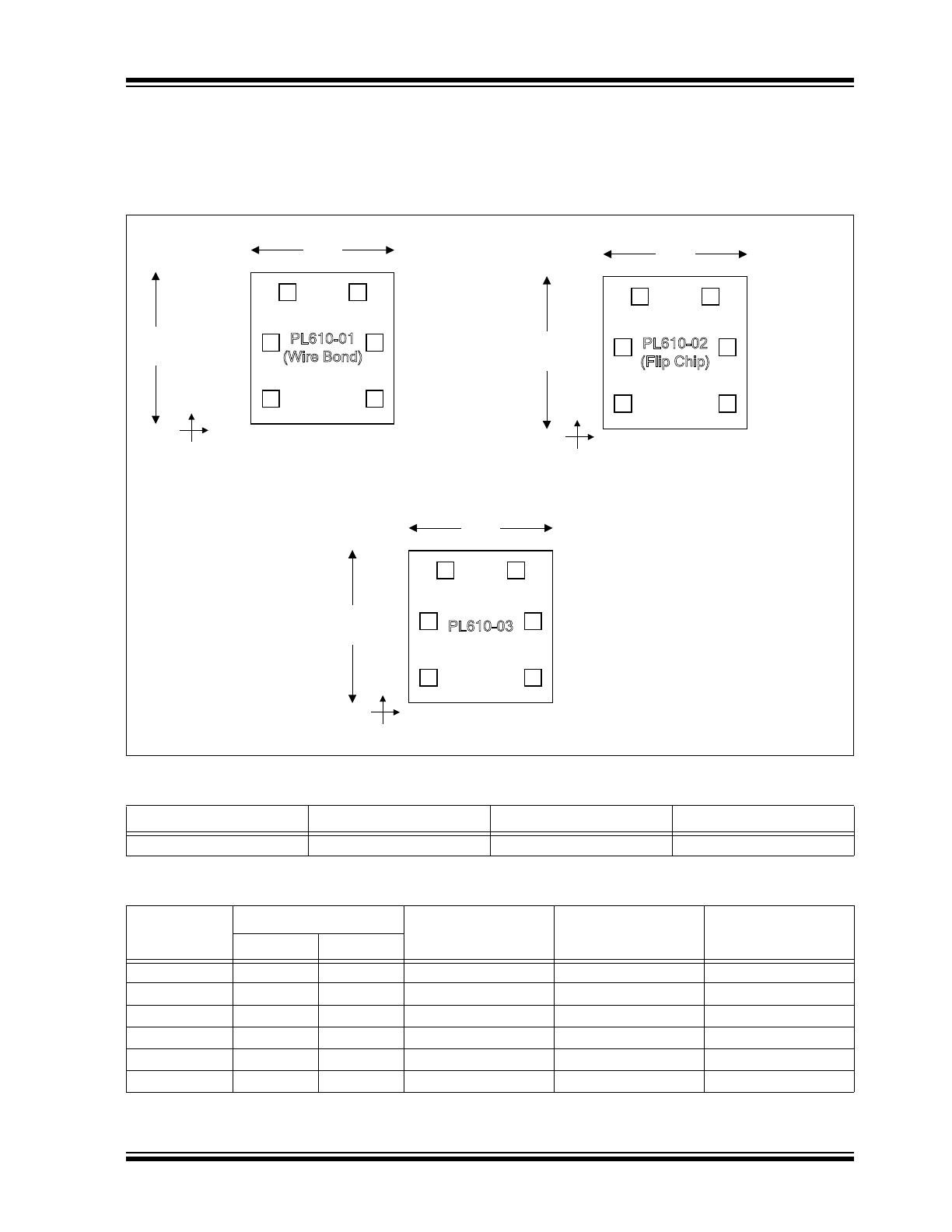
2.0
PAD DESCRIPTIONS
The descriptions of the pads are listed in
Table 2-2
.
Pad Configurations
TABLE 2-1:
DIE SPECIFICATION
Chip Size
Chip Thickness
Pad Size
Chip Base
0.65 mm x 0.60 mm
Optional
90 µm
GND Level
TABLE 2-2:
PAD FUNCTION TABLE
Pad Number
Pad Center
Pad Name
PL610-01
Pad Name
PL610-02
Pad Name
PL610-03
X
Y
1
–177
231
XIN
XOUT
XIN
2
–215
41
OE, PDB, CLK1
VDD
GND
3
–215
–186
GND
CLK0
CLK0
4
215
–186
CLK0
GND
VDD
5
215
41
VDD
OE, PDB, CLK1
OE, PDB, CLK1
6
177
213
XOUT
XIN
XOUT
PL610-01
PL610-02
(650μmx600μm)
0.60
Note: ^ denotes internal pull up
1
XOUT
VDD
CLK0
XIN
OE^, PDB^,
CLK1
GND
PL610-01
(Wire Bond)
0.
65
2
3
6
5
4
X
Y
(650μmx600μm)
0.60
Note: ^ denotes internal pull up
1
XOUT
VDD
CLK0
XIN
OE^, PDB^,
CLK1
GND
PL610-02
(Flip Chip)
0.
65
2
3
6
5
4
X
Y
PL610-03
(650μmx600μm)
Note: ^ denotes internal pull up
1
XIN
GND
CLK0
XOUT
OE^, PDB^,
CLK1
VDD
PL610-03
0.
65
2
3
6
5
4
X
Y
0.60
PL610-01/-02/-03
DS20005616A-page 8
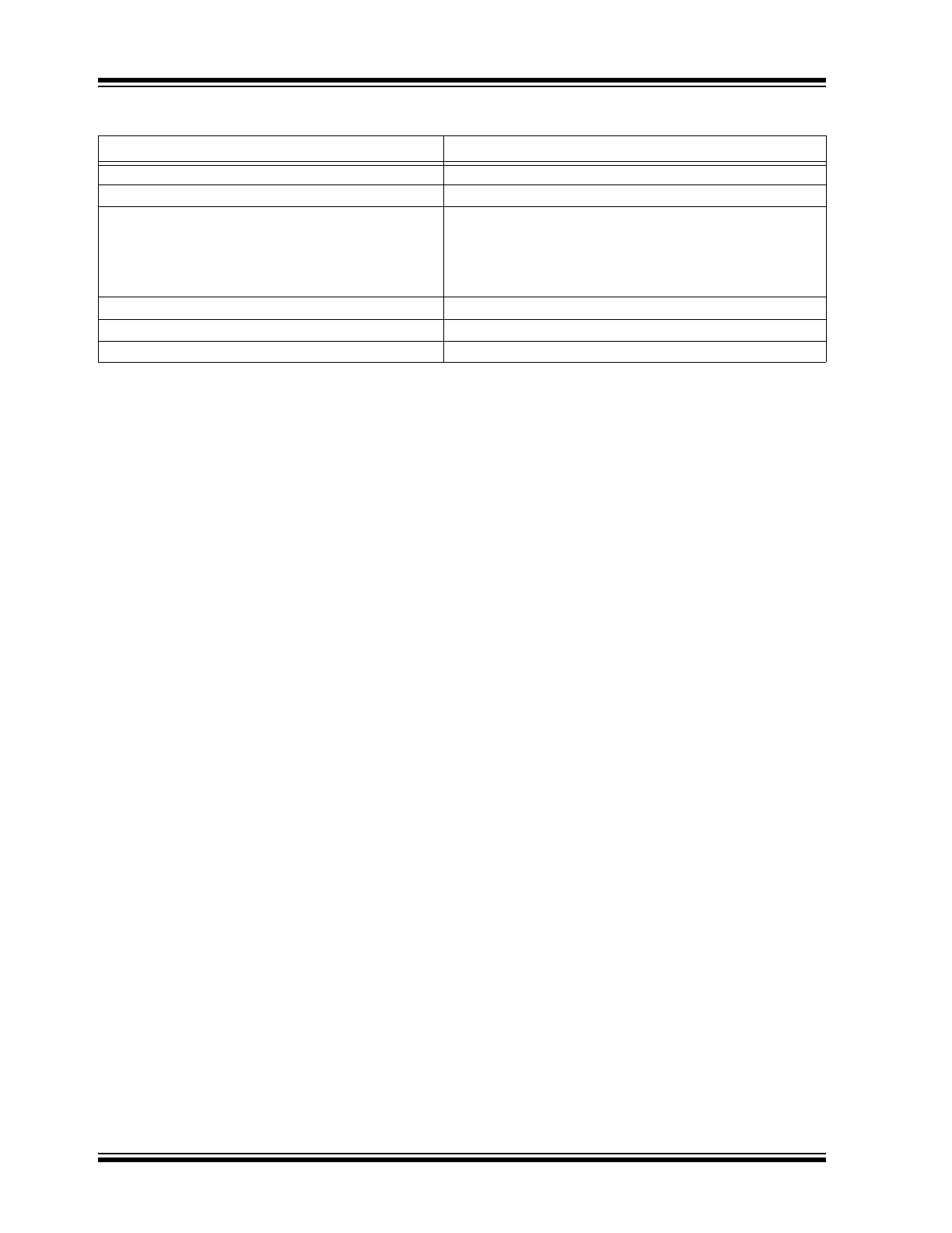
2016 Microchip Technology Inc.
TABLE 2-3:
PAD FUNCTION DESCRIPTIONS
Pad Name
Description
CLK0
Programmable clock output
GND
GND connection
OE^, PDB^, CLK1
Programmable as:
Output Enable (OE) – Enables/Disables CLK0 output buffer
Power Down (PDB) – Enables/Disables CLK0 output buffer
and crystal oscillator circuitry
CLK1 – Second clock output
V
DD
V
DD
connection
XIN
Crystal input pad
XOUT
Crystal output pad
2016 Microchip Technology Inc.
DS20005616A-page 9
PL610-01/-02/-03
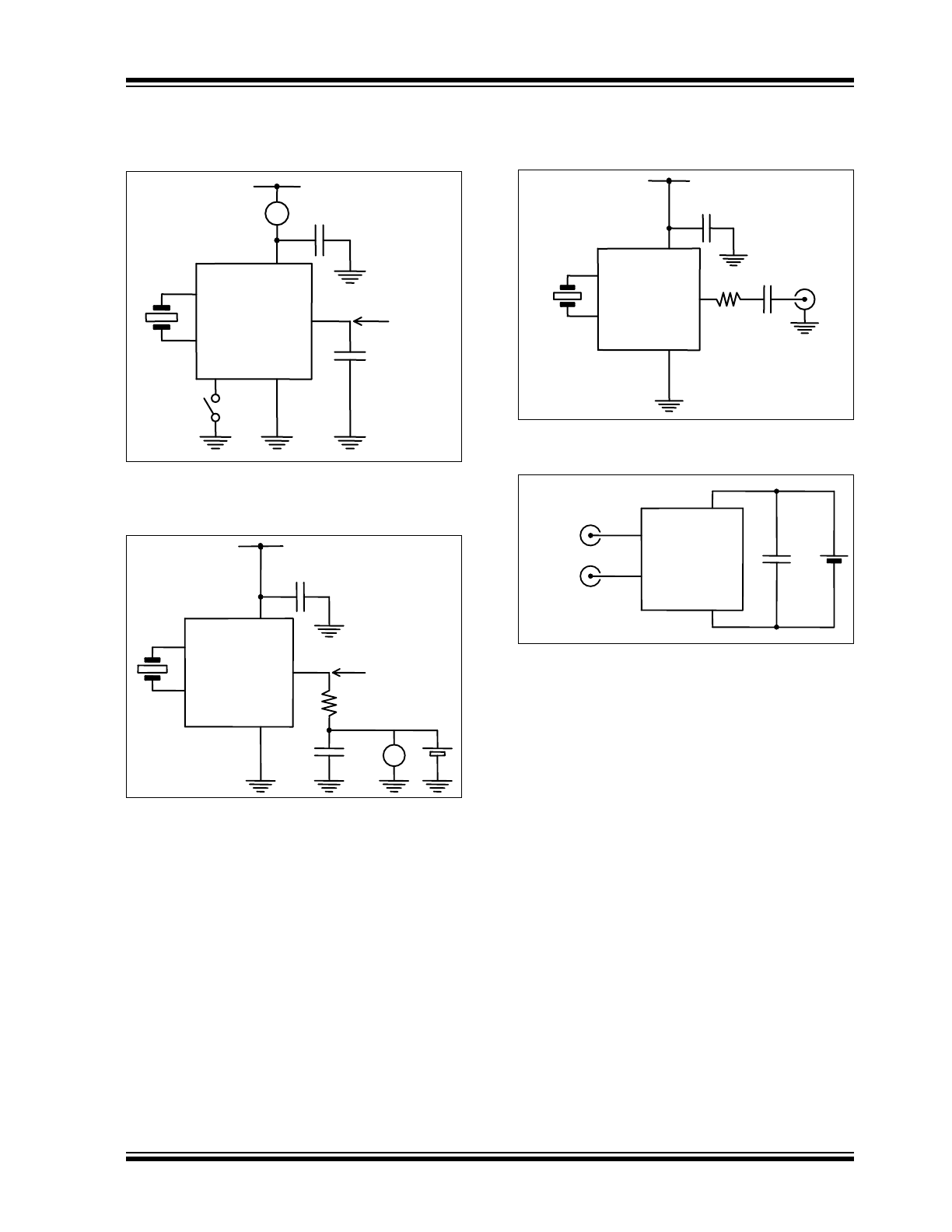
3.0
MEASUREMENT TEST
CIRCUITS (MTC)
FIGURE 3-1:
MTC-1: Rise Time, Fall
Time, Duty Cycle, V
OL
, V
OH
, I
DD
, Power Down
Current, Output Enable/Disable.
FIGURE 3-2:
MTC-2: Output Drive
Current and Output Impedance.
FIGURE 3-3:
MTC-3: Jitter and Phase
Noise.
FIGURE 3-4:
MTC-4: Negative
Resistance.
XIN
VDD
XOUT
GND
CLK
OE^
FET
Probe
CL
A
0.1μF
XOUT
XIN
OE^
Probe
FET
CLK
VDD
GND
0.1μF
0.1μF V
R
XOUT
OE^
GND
0.1μF
XIN
CLK
VDD
0.1μF
XIN
OE^
XOUT
CLK
GND
VDD
0.1μF
Network
Analyzer
PL610-01/-02/-03
DS20005616A-page 10
2016 Microchip Technology Inc.
4.0
WAVEFORM SWITCHING
CHARACTERISTICS
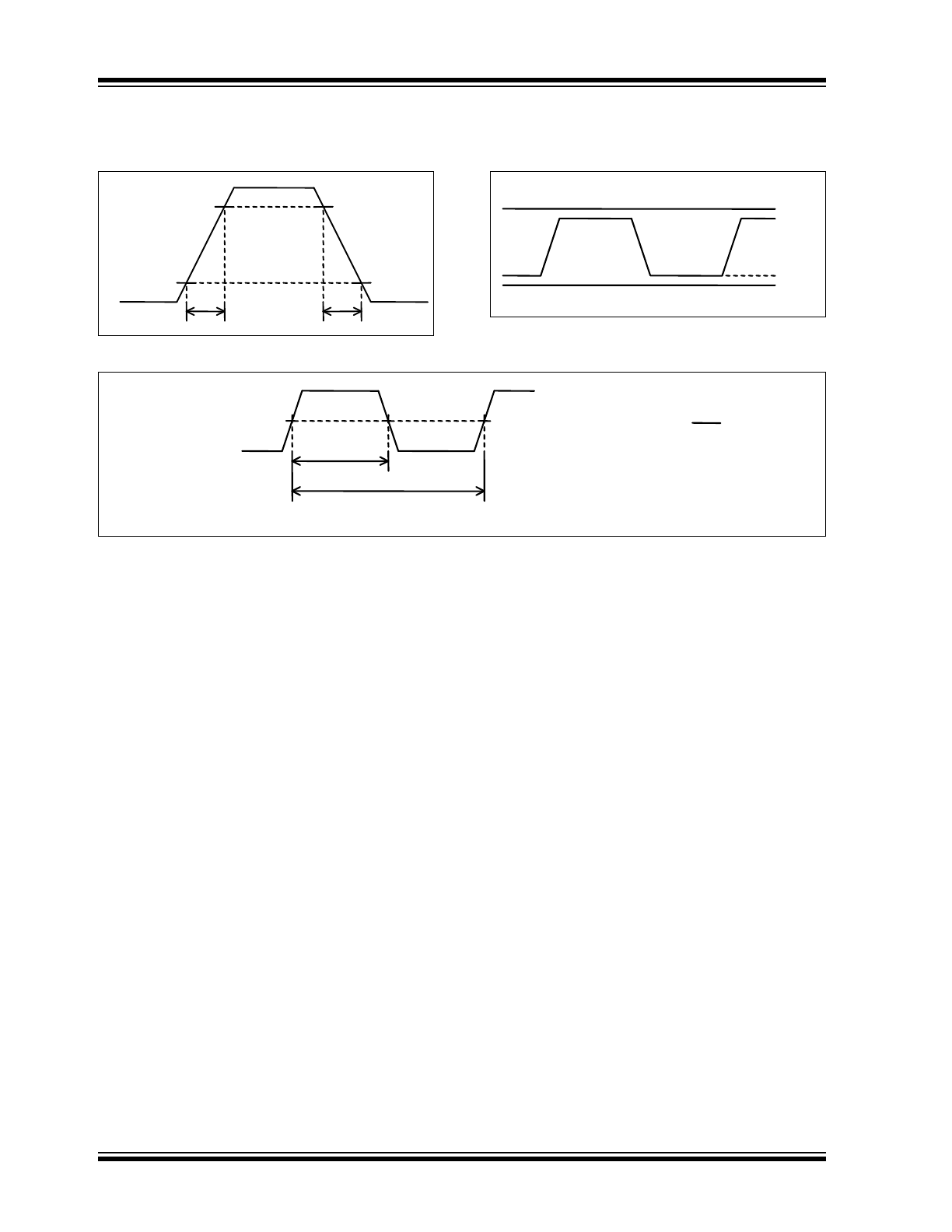
FIGURE 4-1:
Rise and Fall Times.
FIGURE 4-2:
V
OH
, V
OL
.
FIGURE 4-3:
Duty Cycle.
tr
tf
90%V
DD
10% V
DD
GND
VOH
VOL
V
DD
Tw
T
Duty Cycle = 100% × Tw
T
50%
V
DD