
2016 Microchip Technology Inc.
DS20005650A-page 1
PL613-01
Features
• Designed for PCB Space Savings with Three
Low-Power Programmable PLLs and up to 8
Clock Outputs
• Low Power Consumption
- 10 µA Typical When PDB is Activated
• Output Frequency:
- ≤110 MHz at 1.8V Operation
- ≤166 MHz at 2.5V Operation
- ≤200 MHz at 3.3V Operation
• Input Frequency:
- Fundamental Crystal: 10 MHz to 40 MHz
- Reference Input: 10 MHz to 200 MHz
• Programmable I/O Pins Can be Configured as
Output Enable (OE), Configuration Switching
(CSEL), Frequency Switching (FSELX), Power
Down (PDB) Inputs, or Clock Outputs
• Disabled Outputs Programmable as HiZ or Active
Low
• Four Distinct Configurations Selectable with
CSEL[0:1]
• Single 1.8V, 2.5V, or 3.3V ±10% Power Supply
• Temperature range: 0°C to 70°C, –40°C to +85°C
• Available in 3 mm x 3 mm QFN or TSSOP
Packages
General Description
The PL613-01 is an advanced triple PLL design based
on Microchip’s PicoPLL™, the world’s smallest
programmable clock, technology. This advanced
technology allows the eight output PL613-01 to fit in to
a small 3 mm x 3 mm QFN or TSSOP package for high
performance, low-power, low-cost applications.
Besides its small form factor and 8 outputs that can
reduce overall system costs, the PL613-01 offers
superior phase noise, jitter and power consumption
performance.
The power down feature of PL613-01, when activated,
allows the IC to consume less than 10 µA of power,
while its CSEL[0:1] allows switching between up to four
pre-programmed configurations. The FSELX, on the
other hand, allows frequency switching of two outputs
(CLK1 and CLK2) on a single clock pin (CLK2).
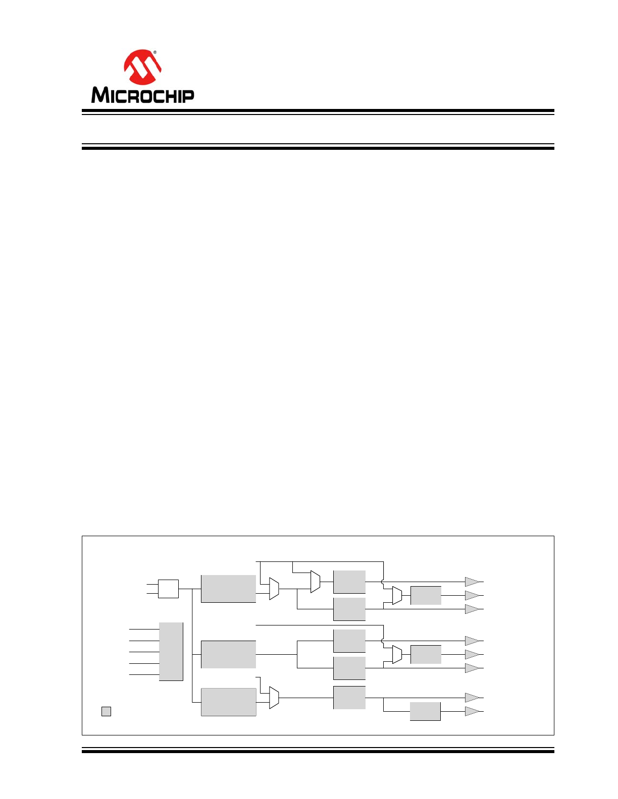
Block Diagram
PL613-01
Programmable Function
Xtal
OSC
XOUT
Programmable
PLL1
XIN/FIN
Programmable
PLL3
CLK4
Odd/Even
Divider
(5-bits)
CLK5, OE6, CSEL0
CLK6, OEM, PDB
CLK7, OE0, CSEL1
VCO1
VCO3
CLK0, FSELX
Odd/Even
Divider
(5-bits)
CLK1, OE2
Odd/Even
Divider
(5-bits)
CLK3, OE4
CLK2
Programmable
PLL2
VCO2
FREF
FREF
÷
1,
÷
2,
÷
4,
÷
8
Odd/Even
Divider
(5-bits)
Odd/Even
Divider
(5-bits)
FREF
FREF
Programming
Interface
Output Drive
PDB
FSELX
OE, OEM
÷
1,
÷
2,
÷
4,
÷
8
÷
1,
÷
2,
÷
4,
÷
8
CSEL[0:1]
1.8V to 3.3V, PicoPLL, 3-PLL, 200 MHz, 8 Output Clock IC

PL613-01
DS20005650A-page 2
2016 Microchip Technology Inc.
1.0
ELECTRICAL CHARACTERISTICS
Absolute Maximum Ratings †
Supply Voltage Range (V
DD
)..................................................................................................................... –0.5V to +4.6V
Input Voltage Range (V
IN
) .................................................................................................................–0.5V to V
DD
+ 0.5V
Output Voltage Range (V
OUT
) ...........................................................................................................–0.5V to V
DD
+ 0.5V
Data Retention at +85°C ..................................................................................................................................... 10 Years
†
Notice: Stresses above those listed under “Absolute Maximum Ratings” may cause permanent damage to the device.
This is a stress rating only and functional operation of the device at those or any other conditions above those indicated
in the operational sections of this specification is not intended. Exposure to maximum rating conditions for extended
periods may affect device reliability.
2016 Microchip Technology Inc.
DS20005650A-page 3
PL613-01
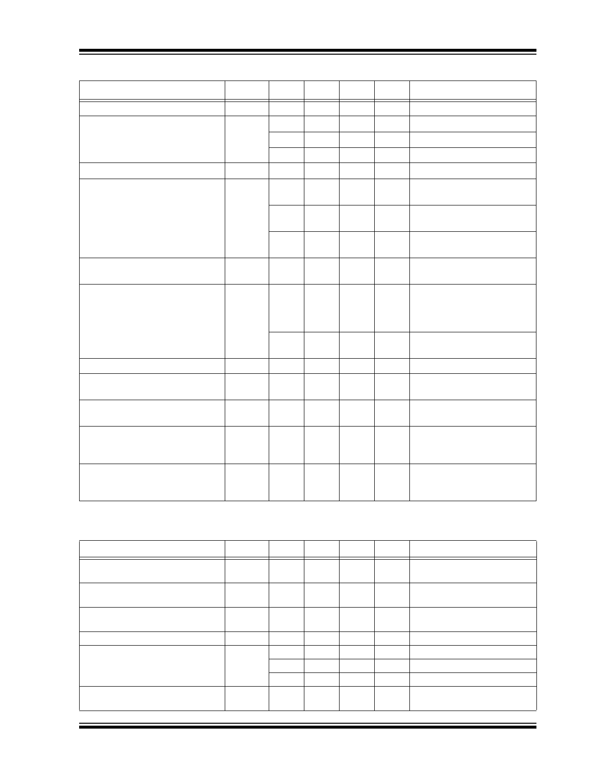
TABLE 1-1:
AC ELECTRICAL CHARACTERISTICS
Parameters
Sym.
Min.
Typ.
Max.
Units
Conditions
Crystal Input Frequency
X
IN
10
—
40
MHz
Fundamental Crystal
Input Frequency
F
IN
10
—
200
MHz
at V
DD
= 3.3V, ±10%
10
—
166
MHz
at V
DD
= 2.5V, ±10%
10
—
110
MHz
at V
DD
= 1.8V, ±10%
Input Signal Amplitude
—
0.8
—
V
DD
V
PP
Internally AC-Coupled
Output Frequency
—
1
—
200
MHz
at V
DD
= 3.3V, ±10%
(High Drive)
1
—
166
MHz
at V
DD
= 2.5V, ±10%
(High Drive)
1
—
110
MHz
at V
DD
= 1.8V, ±10%
(High Drive)
Settling Time
—
—
—
2
ms
At power-up (V
DD
≥ 90% of
operating V
DD
)
Output Enable Time
—
—
—
500
ns
OE function; T
A
= 25°C, 15 pF
load. Add one clock period to
this measurement for a usable
clock output.
—
—
2
ms
PDB function; T
A
= 25°C,
15 pF load.
V
DD
Sensitivity
—
–2
—
2
ppm
Frequency vs. V
DD
, ±10%
Output Rise Time
—
—
1.2
1.7
ns
15 pF load, 10/90% V
DD
, High
Drive, 3.3V
Output Fall Time
—
—
1.2
1.7
ns
15 pF load, 10/90% V
DD
, High
Drive, 3.3V
Duty Cycle
—
45
50
55
%
PLL-driven output, @ V
DD
/2,
15 pF load, High Drive, over
entire frequency range
Period Jitter (
Note 1
)
(10,000 Samples)
—
—
300
—
ps
Configuration-dependent, with
capacitive decoupling between
V
DD
and GND
Note 1:
Jitter performance depends on the programming parameters.
TABLE 1-2:
DC ELECTRICAL CHARACTERISTICS
Parameters
Sym.
Min.
Typ.
Max.
Units
Conditions
Supply Current (V
DD
= 3.3V)
I
DD
—
17
23
mA
All 8 outputs @ 20 MHz
No load
Supply Current (V
DD
= 2.5V)
I
DD
—
13.5
18
mA
All 8 outputs @ 20 MHz
No load
Supply Current (V
DD
= 1.8V)
I
DD
—
9.5
13
mA
All 8 outputs @ 20 MHz
No load
Supply Current
I
DD
—
10
—
µA
When PDB = 0
Operating Voltage
V
DD
2.97
3.3
3.63
V
Configured for 3.3V Operation
2.25
2.5
2.75
V
Configured for 2.5V Operation
1.62
1.8
1.98
V
Configured for 1.8V Operation
Output Low Voltage
V
OL
—
—
0.4
V
I
OL
= +4 mA, Standard Drive,
3.3V
PL613-01
DS20005650A-page 4
2016 Microchip Technology Inc.
Output High Voltage
V
OH
2.4
—
—
V
I
OL
= –4 mA, Standard Drive,
3.3V
Output Current, Low Drive
I
OLD
4
—
—
mA
V
OL
= 0.4V, V
OH
= 2.4V, 3.3V
Output Current, Standard Drive
I
OSD
8
—
—
mA
V
OL
= 0.4V, V
OH
= 2.4V, 3.3V
Output Current, High Drive
I
OHD
16
—
—
mA
V
OL
= 0.4V, V
OH
= 2.4V, 3.3V
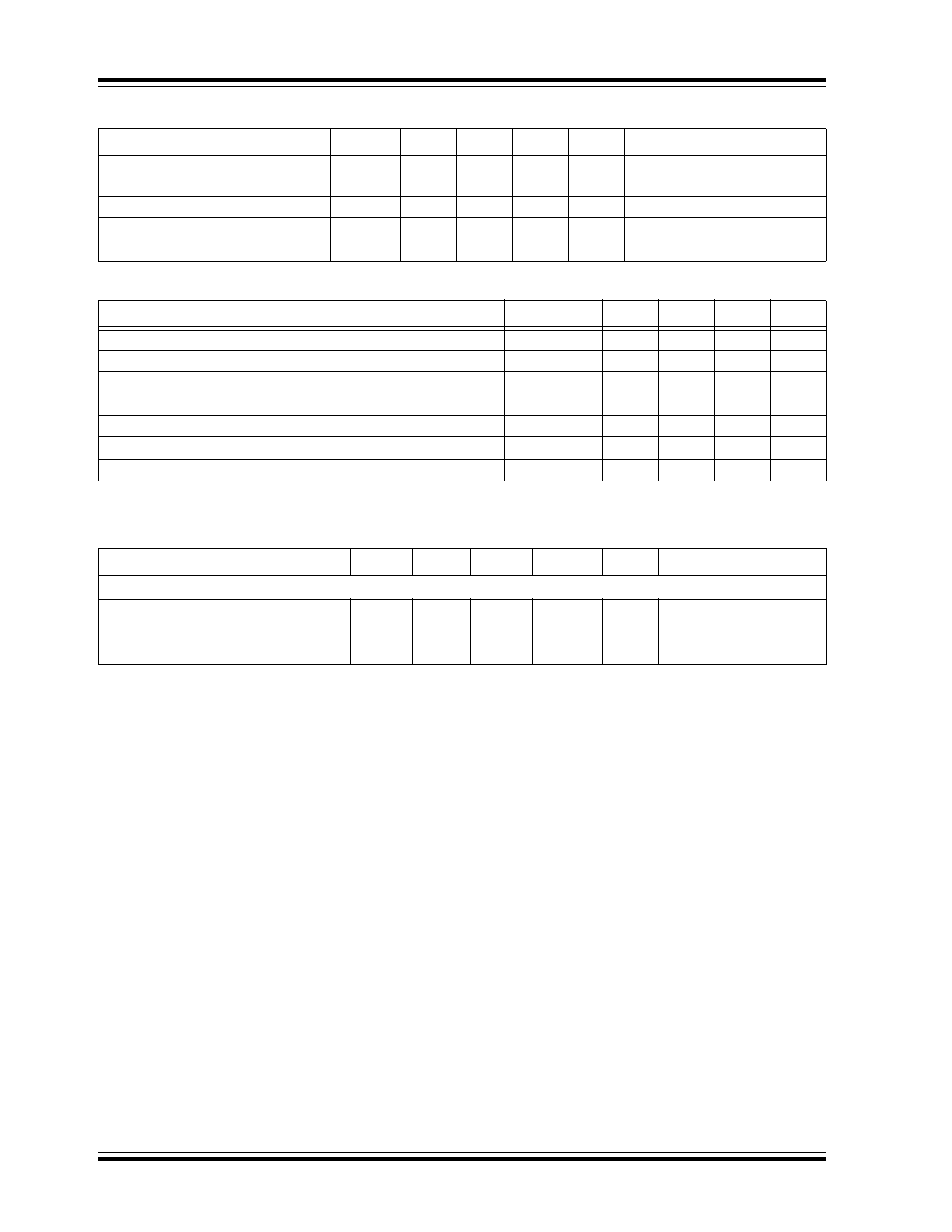
TABLE 1-2:
DC ELECTRICAL CHARACTERISTICS (CONTINUED)
Parameters
Sym.
Min.
Typ.
Max.
Units
Conditions
TABLE 1-3:
CRYSTAL CHARACTERISTICS
Parameters
Symbol
Min.
Typ.
Max.
Units
Fundamental Crystal Resonator Frequency
F
XIN
10
—
40
MHz
Crystal Loading Rating
C
L(XTAL)
—
15
—
pF
Operating Drive Level
—
—
0.1
2
mW
Metal Can Crystal, Shunt Capacitance
C0
—
—
5.5
pF
Metal Can Crystal, ESR Max.
ESR
—
—
40
Ω
Small SMD Crystal, Shunt Capacitance
C0
—
—
2.5
pF
Small SMD Crystal, ESR Max.
ESR
—
—
60
Ω
TEMPERATURE SPECIFICATIONS (
Note 1
)
Parameters
Sym.
Min.
Typ.
Max.
Units
Conditions
Temperature Ranges
Storage Temperature Range
T
S
–65
—
+150
°C
—
Soldering Temperature
—
—
—
+260
°C
—
Ambient Operating Temperature Range
T
A
–40
—
+85
°C
—
Note 1:
Exposure of the device under conditions beyond the limits specified by Maximum Ratings for extended
periods may cause permanent damage to the device and affect product reliability. These conditions
represent a stress rating only, and functional operations of the device at these or any other conditions
above the operational limits noted in this specification is not implied. Operating temperature is guaranteed
by design. Parts are tested to commercial grade only.
2016 Microchip Technology Inc.
DS20005650A-page 5
PL613-01
2.0
PIN DESCRIPTIONS
The descriptions of the pins are listed in
Table 2-1
.
Package Types
Note 1:
^ denotes internal pull-up.
CLK0, FSELX^
VDD
GND
CLK1, OE2^
GND
XIN, FIN
XOUT
VDD
CLK5, OE6^, CSEL0
CLK6, OEM^, PDB^
VDD
CLK7, OE0^, CSEL1
CLK4
CLK3, OE4^
GND
CLK2
1
2
3
4
5
6
7
8
12
11
10
9
16
15
14
13
1
XIN, FIN
GND
CLK5, OE6^, CSEL0
CLK6, OEM^, PDB^
VDD
CLK7, OE0^, CSEL1
CLK0, FSELX
VDD
16 XOUT
VDD
CLK4
CLK3, OE4^
GND
CLK2
CLK1, OE2^
GND
15
14
13
12
11
10
9
2
3
4
5
6
7
8
PL613-01
16-P
IN
QFN
(T
OP
V
IEW
)
PL613-01
16-P
IN
TSSOP
(T
OP
V
IEW
)
TABLE 2-1:
PIN FUNCTION TABLE
Pin Number
QFN-16
Pin Number
TSSOP-16
Pin Name
Pin Type
(
Note 1
)
Description
1
7
CLK0,
FSELX
B
Programmable clock (CLK0) output or CLK2 frequency
switching (FSELX) input.
3, 6, 12
2, 9, 12
GND
P
Ground connection.
2, 9, 15
5, 8, 15
VDD
P
V
DD
connection.
4
10
CLK1,
OE2
B
Programmable clock (CLK1) output or Output Enable
(OE) input for CLK2.
5
11
CLK2
O
Programmable clock (CLK2) output.
7
13
CLK3,
OE4
B
Programmable clock (CLK3) output or Output Enable
(OE) input for CLK4.
8
14
CLK4
O
Programmable clock (CLK4) output.
10
16
XOUT
O
Crystal output pin. Do not connect when using FIN.
11
1
XIN, FIN
I
Crystal or reference clock input.
13
3
CLK5,
OE6,
CSEL0
B
Programmable clock (CLK5) output or Output Enable
(OE) input for CLK6 or configuration switching input.
PL613-01
DS20005650A-page 6
2016 Microchip Technology Inc.
14
4
CLK6,
OEM, PDB
B
Programmable clock (CLK6) output or Output Enable
master (OEM) all clock outputs or power down mode
(PDB) input.
16
6
CLK7,
OE0,
CSEL1
B
Programmable clock (CLK7) output or Output Enable
(OE) input for CLK0 or configuration switching input.
Note 1:
All bidirectional buffers (I/Os) incorporate an internal 60 kΩ pull-up resistor when used as an input, except
when PDB mode is used. In configurations that use PDB, the PDB pin will have a 10 MΩ pull-up resistor.
TABLE 2-2:
KEY PROGRAMMING PARAMETERS
CLK[0:7]
Output Frequency
Output
Drive Strength
Programmable
Input/Output
CLK[0,3,6]:
F
VCOx
/ (P*(1,2,4,8)),
F
REF
, or
F
REF
/ (P*(1,2,4,8))
CLK[1,4,7]:
F
VCOx
/ P
CLK[2,5]:
F
VCOx
/ P,
F
REF
, or
F
REF
/ P
Where F
VCOx
= F
REF
* M / R
M = 11 bit
R = 8 bit
P = 5 bit (odd/even divider)
Each output has three optional drive
strengths to choose from:
• Low: 4 mA
• Standard: 8 mA (default)
• High: 16 mA
Most pins are multi-function I/Os. In
addition to CLK, they can be configured
to perform as the following:
• OE[0,2,4,6]: Output Enable for
Individual I/Os.
• OEM: Master OE Controlling All
Outputs.
• CSEL[0:1]: Device Configuration
Switching.
• FSELX: CLK2 Frequency
Switching.
• PDB: Power Down.
• CLK[0:8]: Output.
• HiZ or Active-Low Disabled State.
TABLE 2-1:
PIN FUNCTION TABLE (CONTINUED)
Pin Number
QFN-16
Pin Number
TSSOP-16
Pin Name
Pin Type
(
Note 1
)
Description
2016 Microchip Technology Inc.
DS20005650A-page 7
PL613-01
3.0
FUNCTIONAL DESCRIPTION
The PL613-01 is a highly featured, very flexible,
advanced triple-PLL design for high performance,
low-power applications. The device accepts a low-cost
fundamental crystal input of 10 MHz to 40 MHz or a
reference clock input of 10 MHz to 200 MHz and is
capable of producing eight distinct output frequencies
up to 200 MHz. All three PLLs are fully programmable,
with a total of five, 5-bit post-VCO, odd/even
‘P-counter’ dividers with an additional 1, 2, 4, or 8 ‘Post
P-counter’ dividers that easily generate the most
demanding frequencies. The outputs can be
programmed to deliver the generated frequencies from
the PLLs or the reference input. Each bidirectional
feature pin (I/O) on the PL613-01 incorporates a 60 kΩ
pull-up resistor and can be configured to perform
various functions. Usage of various design features of
these products is mentioned in the following
paragraphs.
3.1
PLL Programming
The three PLLs in PL613-01 are fully programmable.
Each PLL is equipped with an 8-bit input frequency
divider (R-Counter) and an 11-bit VCO frequency
feedback loop (M-Counter) divider. The three PLL
outputs are transferred to five 5-bit post-VCO,
odd/even dividers (P-Counter), as shown in the
Block
Diagram
. In addition, there are three optional (÷1, ÷2,
÷4, or ÷8) post P-Counter dividers that can further
divide the VCO frequency. In general, the PLL output
frequency is determined by the following formula:
EQUATION 3-1:
For output calculations, please note that ‘P’ includes
the P-Counter bits plus the additional optional dividers
(÷1, ÷2, ÷4, or ÷8), if used.
3.2
CLKx (Clock Outputs)
There are a maximum of eight outputs available on the
PL613-01. Clock output frequencies can be configured
as follows:
• CLK[0,3,6]
- F
VCOx
/ (P*(1, 2, 4, 8))
- F
REF
(Crystal or Reference Clock frequency)
- F
REF
/ (P*(1,2,4,8))
• CLK[1, 7]
- F
VCOx
/ P
• CLK[2, 4, 5]
- F
VCOx
/ P
- F
REF
- F
REF
/ P
Each output can be programmed with a 4 mA, 8 mA, or
16 mA drive strength. The maximum output frequency
is 200 MHz at 3.3V, 166 MHz at 2.5V, or 110 MHz at
1.8V.
3.3
OE (Output Enable)
Four pins can be configured as OE inputs for
controlling individual clock outputs, as show in the table
below.
Typical enable time is <500 ns plus one clock period.
The OE feature can be programmed to allow the output
to float (HiZ) or to operate in active-low mode. The
programming control for individual OEs is show below.
3.4
OEM (Master Output Enable)
One pin can be configured to be a single Master OE
(OEM) input pin that controls all the outputs of the
PL613-01. In addition, the state of the disabled outputs
can be programmed to float (HiZ) or to operate in
active-low mode. The OEM function operates on the
following logic:
Typical enable time is <500 ns plus one clock period.
F
OUT
F
REF
M
R P
=
OEx
Controls Output on
CLK#
OE0
CLK0
OE2
CLK2
OE4
CLK4
OE6
CLK6
OE
Pin
OE Type
(Programmable)
Osc
PLL Output
0
0 (default)
On
On
HiZ
1
On
On
Active
0
1
Normal Operation (default)
OE
Pin
OE Type
(Programmable)
Osc
PLL Output
0
0 (default)
On
On
HiZ
1
On
On
Active
0
1
Normal Operation (default)
PL613-01
DS20005650A-page 8
2016 Microchip Technology Inc.
3.5
PDB (Power Down Control)
When activated, PDB disables all the PLLs, the
oscillator circuitry, counters, and all other active
circuitry. PDB activation disables all outputs and the IC
consumes <10 µA of power. The PDB input
incorporates a 10 MΩ pull-up resistor for normal
operation.
The PDB feature can be programmed to allow the
output to float (HiZ) or to operate in active-low mode.
The logic for PDB is shown in the following table:
Typical enable time from power down in <2 ms.
3.6
CSEL (On-the-Fly Configuration
Switching)
The PL613-01 can be programmed to allow switching
between four different configurations, allowing for
changes in the output frequencies. Many applications
(i.e. video/audio) can use the same design footprint,
but allow for configuration switching, adhering to
various standards. CSEL0 and CSEL1 are used in the
switching selection. These pins incorporate a 60 kΩ
pull-up resistor for normal operation. The logic for
configuration switching of the programmed parts is
shown below:
Typical enable time is <500 µs.
3.7
FSELX (On-the-Fly Output
Frequency Switching Between
Two Output Frequencies)
The PL613-01 is equipped with the FSELX feature to
allow frequency switching between two frequencies on
one of the output pins. Frequencies assigned to CLK1
and CLK2 can be switched when FSELX is activated
on CLK2 output. The logic for FSELX is shown below:
Typical enable time is <10 ns plus one clock period.
PDB
Pin
PDB Type
(Programmable)
Osc
PLL Output
0
0 (default)
Off
Off
HiZ
1
Off
Off
Active
0
1
Normal Operation (default)
CSEL1
CSEL0
Programmed Configuration
0
0
0
0
1
1
1
0
2
1
1
3 (default)
FSELX
CLK2 Output
0
Frequency 2
1 (default)
Frequency 1
2016 Microchip Technology Inc.
DS20005650A-page 9
PL613-01
4.0
LAYOUT RECOMMENDATIONS
The following guidelines are designed to help create a
performance-optimized PCB design.
4.1
Signal Integrity and Termination
Considerations
• Keep traces short.
• Trace = Inductor. With capacitive loads, this
creates ringing.
• Long trace = long transmission line. Without
proper termination, this causes reflections that
look like ringing.
• Design long traces (greater than one inch) as
striplines or microstrips with defined impedance.
• Match trace at one side to avoid reflections
bouncing back and forth.
4.2
Decoupling and Power Supply
Considerations
• Place decoupling capacitors as close as possible
to the V
DD
pin(s) to limit noise from the power
supply.
• Multiple V
DD
pins should be decoupled separately
for best performance.
• The addition of resistors in series with V
DD
can
help prevent noise from other board sources.
- Traditionally, ferrite beads are used for this
purpose, but with the PL613-01 the results
are better when using resistors.
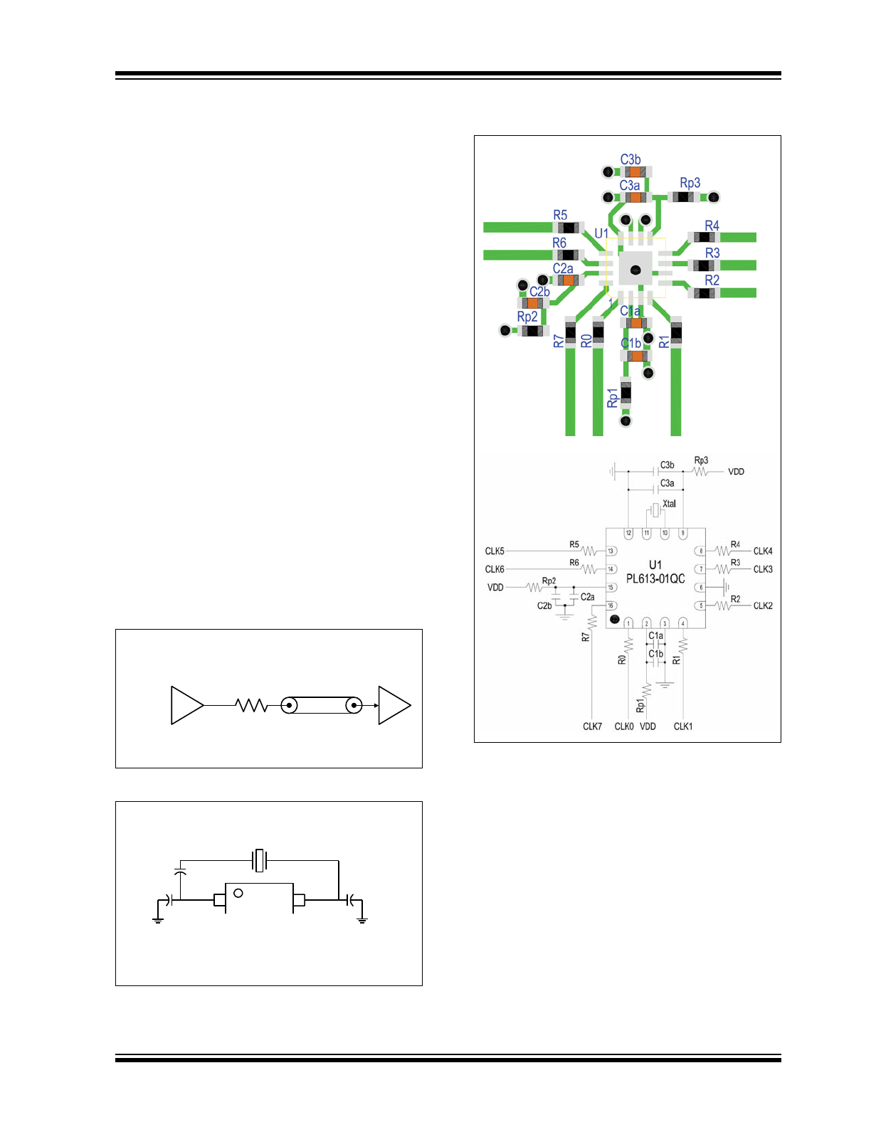
FIGURE 4-1:
Typical CMOS Termination.
FIGURE 4-2:
Crystal Tuning Circuit.
4.3
Layout Example
FIGURE 4-3:
PL613-01 Layout Example.
U1 = PL613-01 in QFN-16L. In this example, all eight
outputs are used.
C1a, C2a, C3a = 0.1 μF and C1b, C2b, C3b = 1 μF for
power supply decoupling. The vias connected to the
capacitors go to the ground plane inside the PCB.
Rp1, Rp2, Rp3 = 10Ω for power supply filtering. The
power supply filter is a first order low pass filter with
–3 dB at 30 kHz. It is important that the frequencies of
the loop bandwidth of the PLLs are filtered properly.
The loop bandwidth of the PLLs is in the range of
100 kHz to 1 MHz depending upon the programmed
configuration. The vias connected to Rp1, Rp2, and
Rp3 go to the V
DD
plane inside the PCB.
R0 ~ R7 = 30Ω for matching CLK0 ~ CLK7 outputs to
the PCB trace impedance. Place the resistors as close
as possible to the IC pins and design the traces to the
Typical CMOS Termination
Place Series Resistor as close as possible to CMOS output.
CMOS Output Buffer
7\SLFDOEXIIHULPSHGDQFHȍ
To CMOS Input
Series Resistor
Use value to match output buffer impedance
WRȍWUDFH7\SLFDOYDOXHLVȍ
ȍ/LQH
Crystal Tuning Circuit
Series and parallel capacitors used to fine tune the crystal load to the circuit load.
Crystal
XIN
1
8
XOUT
CPT
CPT
CST
CST: Series Capacitor that is used to lower circuit load to match crystal load. Raises
frequency offset. This can be eliminated by using a crystal with a C
LOAD
of equal or
greater value than the oscillator.
CPT: Parallel Capacitors that are used to raise the circuit load to match the crystal load.
Lowers frequency offset.
CLK4
CLK3
CLK2
CLK5
CLK6
CL
K7
CL
K0
CL
K1

PL613-01
DS20005650A-page 10
2016 Microchip Technology Inc.
target clock inputs as transmission lines (microstrip or
stripline) for the best signal integrity and the lowest
EMI.
When using ferrite beads instead of Rp1, Rp2, or Rp3,
make sure the resonance frequency of the bead with
the decoupling capacitors is below 50 kHz so as not to
interfere with the PLL loop bandwidth. This requirement
is difficult to fulfill, so it is recommended to use the
resistors Rp1, Rp2, and Rp3 for power supply filtering.