
2017 Microchip Technology Inc.
DS20005529B-page 1
DSC1001/3/4
Features
• Frequency Range: 1 MHz to 150 MHz
• Exceptional Stability over Temperature
- ±10 ppm, ±20 ppm, ±25 ppm, ±50 ppm
• Operating Voltage
- 1.7 to 3.6V
• Operating Temperature Range
- Ext. Industrial –40°C to 105°C
- Industrial –40°C to 85°C
- Commercial –20°C to 70°C
• Low Operating and Standby Current
- 6 mA Operating (1 MHz)
- 15 µA Standby (Max.)
• Ultra Miniature Footprint
- 2.5 mm x 2.0 mm x 0.85 mm
- 3.2 mm x 2.5 mm x 0.85 mm
- 5.0 mm x 3.2 mm x 0.85 mm
- 7.0 mm x 5.0 mm x 0.85 mm
• MIL-STD 883 Shock and Vibration Resistant
• Pb Free, RoHS, Reach SVHC Compliant
• AEC-Q100 Reliability Qualified
Applications
• Mobile Applications
• Consumer Electronics
• Portable Electronics
• DVR, CCTV, Surveillance Cameras
• Low Profile Applications
• Industrial Applications
Benefits
• Pin for Pin “Drop-In” Replacement for Industry
Standard Oscillators
• Semiconductor Level Reliability, Significantly
Higher than Quartz
• Short Mass Production Lead Times
• Longer Battery Life/Reduced Power Consumption
• Compact Plastic Package
• Cost Effective
General Description
The DSC1001/3/4 is a silicon MEMS based CMOS
family of oscillators that offers excellent jitter and
stability performance over a wide range of supply
voltages and temperatures. The device operates from
1 MHz to 150 MHz with supply voltages between 1.8 to
3.3 volts and temperature ranges up to –40°C to
105°C.
The DSC1001/3/4 incorporate an all silicon resonator
that is extremely robust and nearly immune to stress
related fractures, common to crystal based oscillators.
Without sacrificing the performance and stability
required of today’s systems, a crystal-less design
allows for a higher level of reliability, making the
DSC1001/3/4 ideal for rugged, industrial, and portable
applications where stress, shock, and vibration can
damage quartz crystal based systems.
Available in industry standard packages, the
DSC1001/3/4 can be “dropped-in” to the same PCB
footprint as standard crystal oscillators.
The DSC1003 and DSC1004 have the same
functionality and performance as the DSC1001, but
feature higher output drives of 25 pF and 40 pF,
respectively.
Package Types
DSC1001/3/4
CDFN/DFN
(Top View)
STANDBY#
1
2
4
3
GND
VDD
OUT
1.8V-3.3V Low-Power Precision CMOS Oscillators
DSC1001/3/4
DS20005529B-page 2
2017 Microchip Technology Inc.
Block Diagram
PFD
VCO
FRAC
-N
PLL
OUTPUT
V
DD
GND
(PIN1)
STANDBY#
PFD
VCO
FRAC-N
PFD
VCO
PLL
RESONATOR
V
DD
GND
(PIN1)
2017 Microchip Technology Inc.
DS20005529B-page 3
DSC1001/3/4
1.0
ELECTRICAL CHARACTERISTICS
Absolute Maximum Ratings †
Input Voltage (V
IN
) ............................................................................................................................–0.3V to V
DD
+ 0.3V
ESD Protection ....................................................................................................... 4 kV HBM, ±200V MM, 1.5 kV CDM
Recommended Operating Conditions
Supply Voltage (V
DD
) ................................................................................................................................ +1.7V to +3.6V
Output Load (Z
L
) ............................................................................................................................. R > 10 kΩ, C ≤ 15 pF
†
Notice: Stresses above those listed under “Absolute Maximum Ratings” may cause permanent damage to the device.
This is a stress rating only and functional operation of the device at those or any other conditions above those indicated
in the operational sections of this specification is not intended. Exposure to maximum rating conditions for extended
periods may affect device reliability.
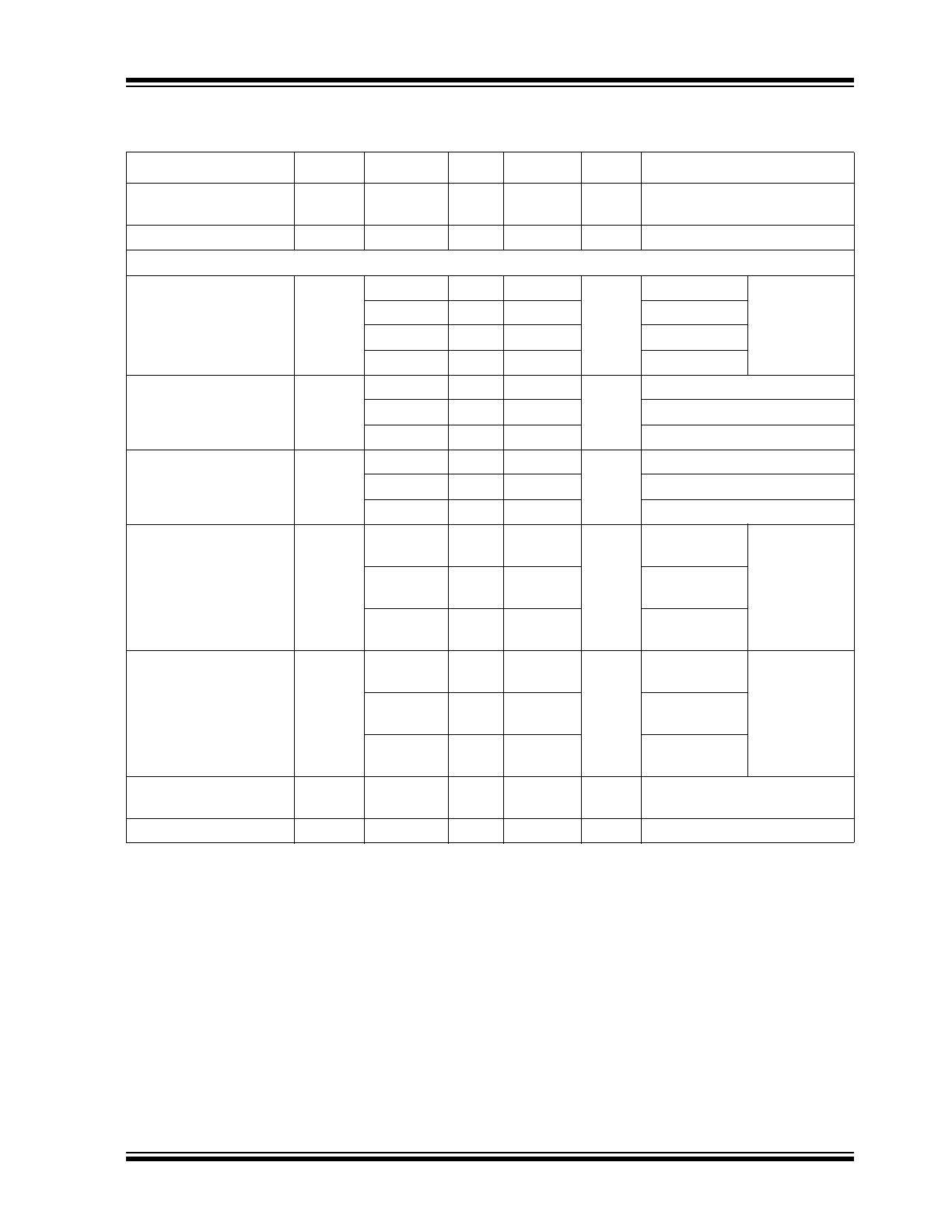
TABLE 1-1:
DC CHARACTERISTICS
Electrical Characteristics:
V
DD
= 1.8 to 3.3V; T
A
= +85°C unless otherwise specified.
Parameters
Sym.
Min.
Typ.
Max.
Units
Conditions
Frequency
F
0
1
—
150
MHz
Single Frequency
Frequency Tolerance
∆f
—
—
±10
ppm
Includes frequency variations
due to initial tolerance,
temperature and power supply
voltage
—
—
±20
—
—
±25
—
—
±50
Aging
∆f
—
—
±5
ppm
1 year @ +25°C
Supply Current, Standby
I
DD
—
—
15
µA
T = +25°C
Output Startup Time
(
Note 1
)
t
SU
—
1.0
1.3
ms
T = +25°C
Output Disable Time
t
DA
—
20
100
ns
—
Output Duty Cycle
SYM
45
—
55
%
—
Input Logic Level High
V
IH
0.75 x V
DD
—
—
V
—
Input Logic Level Low
V
IL
—
—
0.25 x V
DD
V
—
V
DD
= 1.8V
Supply Current, No Load
I
DD
—
6.0
6.3
mA
1 MHz
C
L
= 0 pF,
R
L
= ∞,
T = +25°C
—
6.5
7.1
27 MHz
—
7.2
8.5
70 MHz
—
8.3
11.9
150 MHz
Output Logic Level High
V
OH
0.8 x V
DD
—
—
V
–6 mA, DSC1004, C
L
= 40 pF
0.8 x V
DD
—
—
–6 mA, DSC1003, C
L
= 25 pF
0.8 x V
DD
—
—
–4 mA, DSC1001, C
L
= 15 pF
Output Logic Level Low
V
OL
—
—
0.2 x V
DD
V
6 mA, DSC1004, C
L
= 40 pF
—
—
0.2 x V
DD
6 mA, DSC1003, C
L
= 25 pF
—
—
0.2 x V
DD
4 mA, DSC1001, C
L
= 15 pF
Note 1:
t
SU
is time to stable output frequency after V
DD
is applied. t
SU
and t
EN
(after EN is asserted) are identical
values.
2:
Measured over 50k clock cycles.
DSC1001/3/4
DS20005529B-page 4
2017 Microchip Technology Inc.
Output Transition Rise
Time
t
R
—
1.4
3.0
ns
DSC1001, C
L
=
15 pF
T = +25°C,
20% to 80%
—
1.5
3.0
DSC1003, C
L
=
25 pF
—
1.8
3.0
DSC1004, C
2
=
40 pF
Output Transition Fall
Time
t
F
—
1.0
3.0
ns
DSC1001, C
L
=
15 pF
T = +25°C,
20% to 80%
—
1.1
3.0
DSC1003, C
L
=
25 pF
—
1.2
3.0
DSC1004, C
2
=
40 pF
Jitter, Max.
Cycle-to-Cycle
J
CC
—
60
—
ps
f = 100 MHz (
Note 2
)
Period Jitter
J
P
—
10
15
ps
RMS
f = 100 MHz (
Note 2
)
V
DD
= 2.5V
Supply Current, No Load
I
DD
—
6.0
6.4
mA
1 MHz
C
L
= 0 pF,
R
L
= ∞,
T = +25°C
—
6.7
7.5
27 MHz
—
7.7
9.4
70 MHz
—
9.6
13.9
150 MHz
Output Logic Level High
V
OH
0.9 x V
DD
—
—
V
–6 mA, DSC1004, C
L
= 40 pF
0.8 x V
DD
—
—
–6 mA, DSC1003, C
L
= 25 pF
0.8 x V
DD
—
—
–4 mA, DSC1001, C
L
= 15 pF
Output Logic Level Low
V
OL
—
—
0.1 x V
DD
V
6 mA, DSC1004, C
L
= 40 pF
—
—
0.2 x V
DD
6 mA, DSC1003, C
L
= 25 pF
—
—
0.2 x V
DD
4 mA, DSC1001, C
L
= 15 pF
Output Transition Rise
Time
t
R
—
1.0
2.0
ns
DSC1001, C
L
=
15 pF
T = +25°C,
20% to 80%
—
1.1
2.0
DSC1003, C
L
=
25 pF
—
1.2
2.0
DSC1004, C
2
=
40 pF
Output Transition Fall
Time
t
F
—
0.9
2.0
ns
DSC1001, C
L
=
15 pF
T = +25°C,
20% to 80%
—
1.0
2.0
DSC1003, C
L
=
25 pF
—
1.1
2.0
DSC1004, C
2
=
40 pF
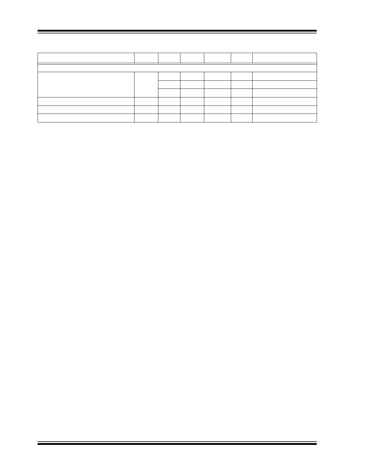
TABLE 1-1:
DC CHARACTERISTICS (CONTINUED)
Electrical Characteristics:
V
DD
= 1.8 to 3.3V; T
A
= +85°C unless otherwise specified.
Parameters
Sym.
Min.
Typ.
Max.
Units
Conditions
Note 1:
t
SU
is time to stable output frequency after V
DD
is applied. t
SU
and t
EN
(after EN is asserted) are identical
values.
2:
Measured over 50k clock cycles.
2017 Microchip Technology Inc.
DS20005529B-page 5
DSC1001/3/4
Jitter, Max.
Cycle-to-Cycle
J
CC
—
50
—
ps
f = 100 MHz (
Note 2
)
Period Jitter
J
P
—
5
10
ps
RMS
f = 100 MHz (
Note 2
)
V
DD
= 3.3V
Supply Current, No Load
I
DD
—
6.0
6.5
mA
1 MHz
C
L
= 0 pF,
R
L
= ∞,
T = +25°C
—
6.8
8.0
27 MHz
—
8.2
10.5
70 MHz
—
10.8
16.6
150 MHz
Output Logic Level High
V
OH
0.9 x V
DD
—
—
V
–8 mA, DSC1004, C
L
= 40 pF
0.9 x V
DD
—
—
–6 mA, DSC1003, C
L
= 25 pF
0.8 x V
DD
—
—
–4 mA, DSC1001, C
L
= 15 pF
Output Logic Level Low
V
OL
—
—
0.1 x V
DD
V
8 mA, DSC1004, C
L
= 40 pF
—
—
0.1 x V
DD
6 mA, DSC1003, C
L
= 25 pF
—
—
0.2 x V
DD
4 mA, DSC1001, C
L
= 15 pF
Output Transition Rise
Time
t
R
—
1.0
2.0
ns
DSC1001, C
L
=
15 pF
T = +25°C,
20% to 80%
—
1.1
2.0
DSC1003, C
L
=
25 pF
—
1.2
2.0
DSC1004, C
2
=
40 pF
Output Transition Fall
Time
t
F
—
0.9
2.0
ns
DSC1001, C
L
=
15 pF
T = +25°C,
20% to 80%
—
1.0
2.0
DSC1003, C
L
=
25 pF
—
1.1
2.0
DSC1004, C
2
=
40 pF
Jitter, Max.
Cycle-to-Cycle
J
CC
—
50
—
ps
f = 100 MHz (
Note 2
)
Period Jitter
J
P
—
5
10
ps
RMS
f = 100 MHz (
Note 2
)
TABLE 1-1:
DC CHARACTERISTICS (CONTINUED)
Electrical Characteristics:
V
DD
= 1.8 to 3.3V; T
A
= +85°C unless otherwise specified.
Parameters
Sym.
Min.
Typ.
Max.
Units
Conditions
Note 1:
t
SU
is time to stable output frequency after V
DD
is applied. t
SU
and t
EN
(after EN is asserted) are identical
values.
2:
Measured over 50k clock cycles.
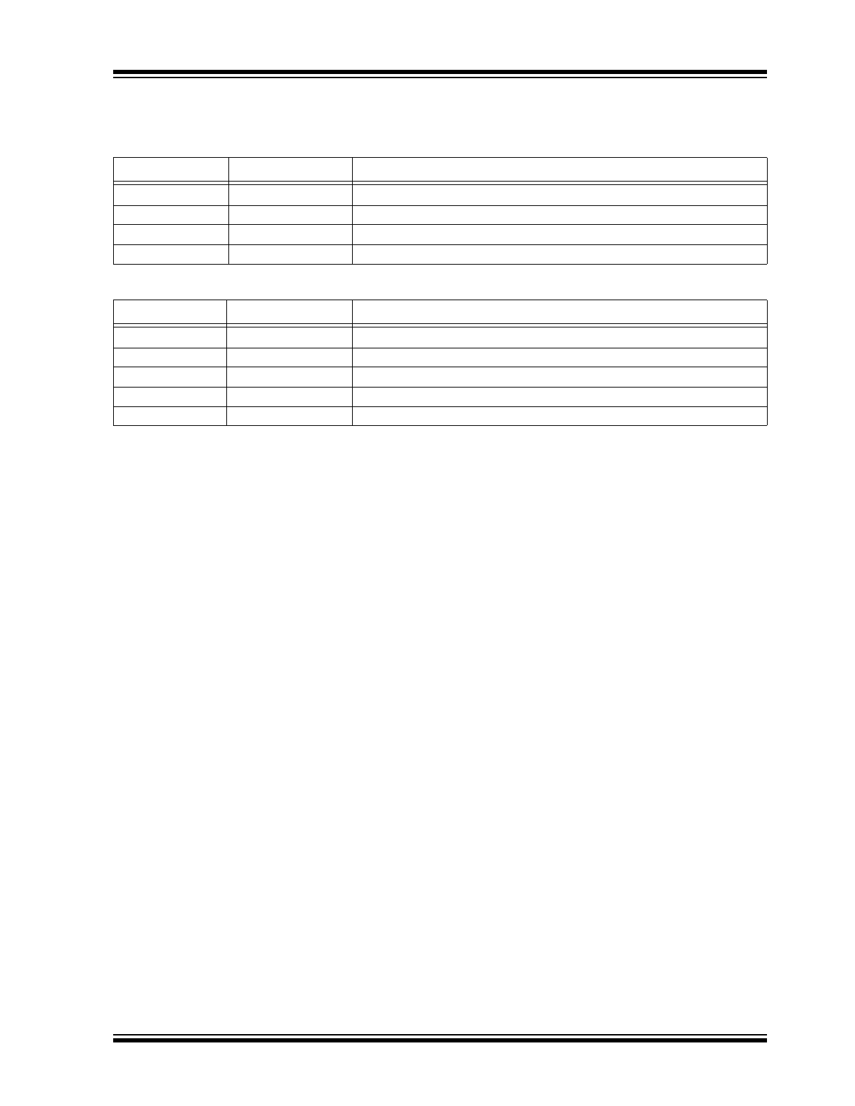
TEMPERATURE SPECIFICATIONS (
Note 1
)
Parameters
Sym.
Min.
Typ.
Max.
Units
Conditions
Temperature Ranges
Operating Temperature Range (T)
T
A
–40
—
+105
°C
Ordering Option L
–40
—
+85
°C
Ordering Option I
–20
—
+70
°C
Ordering Option E
Junction Operating Temperature
T
J
—
—
+150
°C
—
Storage Temperature Range
T
A
–55
—
+150
°C
—
Soldering Temperature Range
T
S
—
—
+260
°C
40 sec. max
Note 1:
The maximum allowable power dissipation is a function of ambient temperature, the maximum allowable
junction temperature and the thermal resistance from junction to air (i.e., T
A
, T
J
,
JA
). Exceeding the
maximum allowable power dissipation will cause the device operating junction temperature to exceed the
maximum +150°C rating. Sustained junction temperatures above +150°C can impact the device reliability.
DSC1001/3/4
DS20005529B-page 6
2017 Microchip Technology Inc.
2017 Microchip Technology Inc.
DS20005529B-page 7
DSC1001/3/4
2.0
PIN DESCRIPTIONS
The descriptions of the pins are listed in
Table 2-1
and
Table 2-2
.
TABLE 2-1:
CDFN PACKAGE PIN FUNCTION TABLE
Pin Number
Symbol
Description
1
STANDBY#
Standby input (Section 4.1 “Standby Function”)
2
GND
Power supply ground
3
OUT
Oscillator output
4
VDD
Positive power supply
TABLE 2-2:
DFN PACKAGE PIN FUNCTION TABLE
Pin Number
Symbol
Description
1
STANDBY#
Standby input (Section 4.1 “Standby Function”)
2
GND
Power supply ground
3
OUT
Oscillator output
4
VDD
Positive power supply
Center Pad
NC
Tie to GND or do not connect.
DSC1001/3/4
DS20005529B-page 8
2017 Microchip Technology Inc.
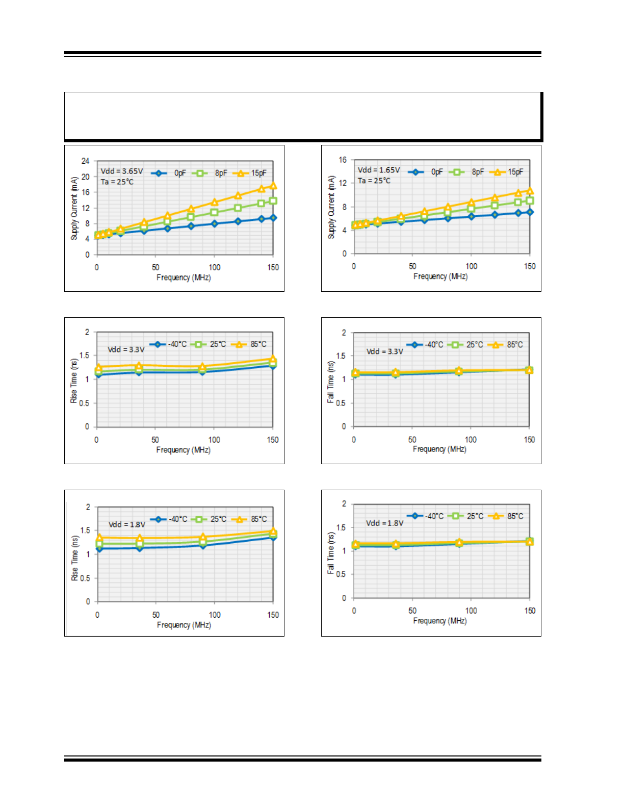
3.0
NOMINAL PERFORMANCE CHARACTERISTICS
Note:
The graphs and tables provided following this note are a statistical summary based on a limited number of
samples and are provided for informational purposes only. The performance characteristics listed herein
are not tested or guaranteed. In some graphs or tables, the data presented may be outside the specified
operating range (e.g., outside specified power supply range) and therefore outside the warranted range.
FIGURE 3-1:
Supply Current.
FIGURE 3-2:
Rise Time.
FIGURE 3-3:
Rise Time.
FIGURE 3-4:
Supply Current.
FIGURE 3-5:
Fall Time.
FIGURE 3-6:
Fall Time.
2017 Microchip Technology Inc.
DS20005529B-page 9
DSC1001/3/4
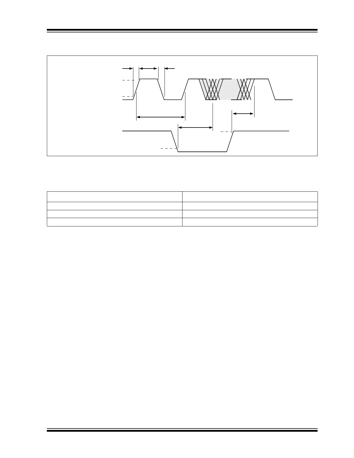
4.0
OUTPUT WAVEFORM
V
IL
1/f
o
OUTPUT
STANDBY#
t
EN
t
DA
t
F
t
R
V
IH
V
OH
V
OL
FIGURE 4-1:
Output Waveform.
4.1
Standby Function
Standby# (Pin 1)
Output (Pin 3)
High Level
Output ON
Open (no connect)
Output ON
Low Level
High Impedance
DSC1001/3/4
DS20005529B-page 10
2017 Microchip Technology Inc.
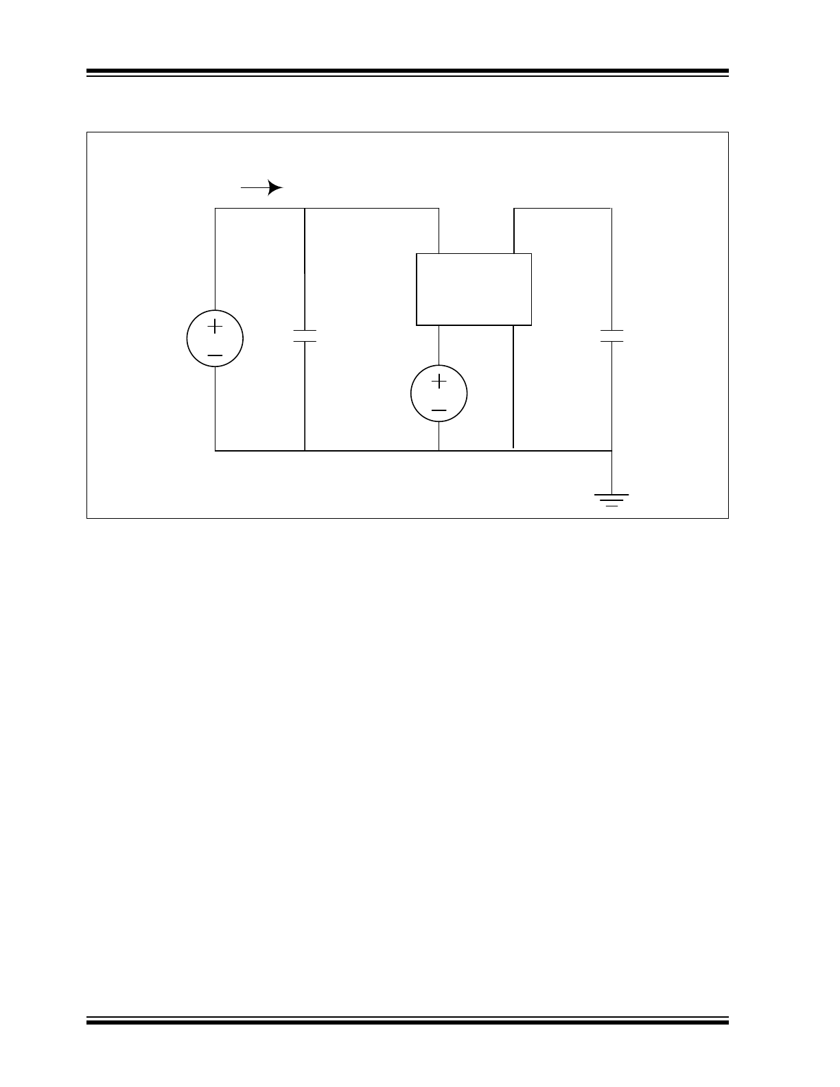
5.0
TEST CIRCUIT
0.01μF
V
DD
15pF
I
DD
*V
SD
4
1
2
3
*V
SD
= Standby# Logic Level Input
FIGURE 5-1:
DSC1001/3/4 Test Circuit.