
2016 Microchip Technology Inc.
DS20005615A-page 1
PL610-01
Features
• Wide Frequency Coverage, Programmable,
Advanced Oscillator Design
• Programmable “Odd/Even” Divider up to ÷63
• Direct Oscillation Operation with Optional
Programmable Features:
- Output Drive Strength (4 mA, 8 mA, or
16 mA)
- 6-bit Odd/Even Output Divider
• Input Frequency:
- Fundamental Crystal: 5 MHz to 130 MHz
- Reference Clock: 1 MHz to 130 MHz
• Supports CMOS or Sine Wave Input Clock
• Output Frequency: 20 kHz to 130 MHz
• Very Low Jitter and Phase Noise
• Low Current Consumption
• Single 1.8V ~ 3.3V ±10% Power Supply
• Operating Temperature Range from –40°C to
+85°C
• Available in 6-pin TDFN or SOT-23
GREEN/RoHS-Compliant Packaging
General Description
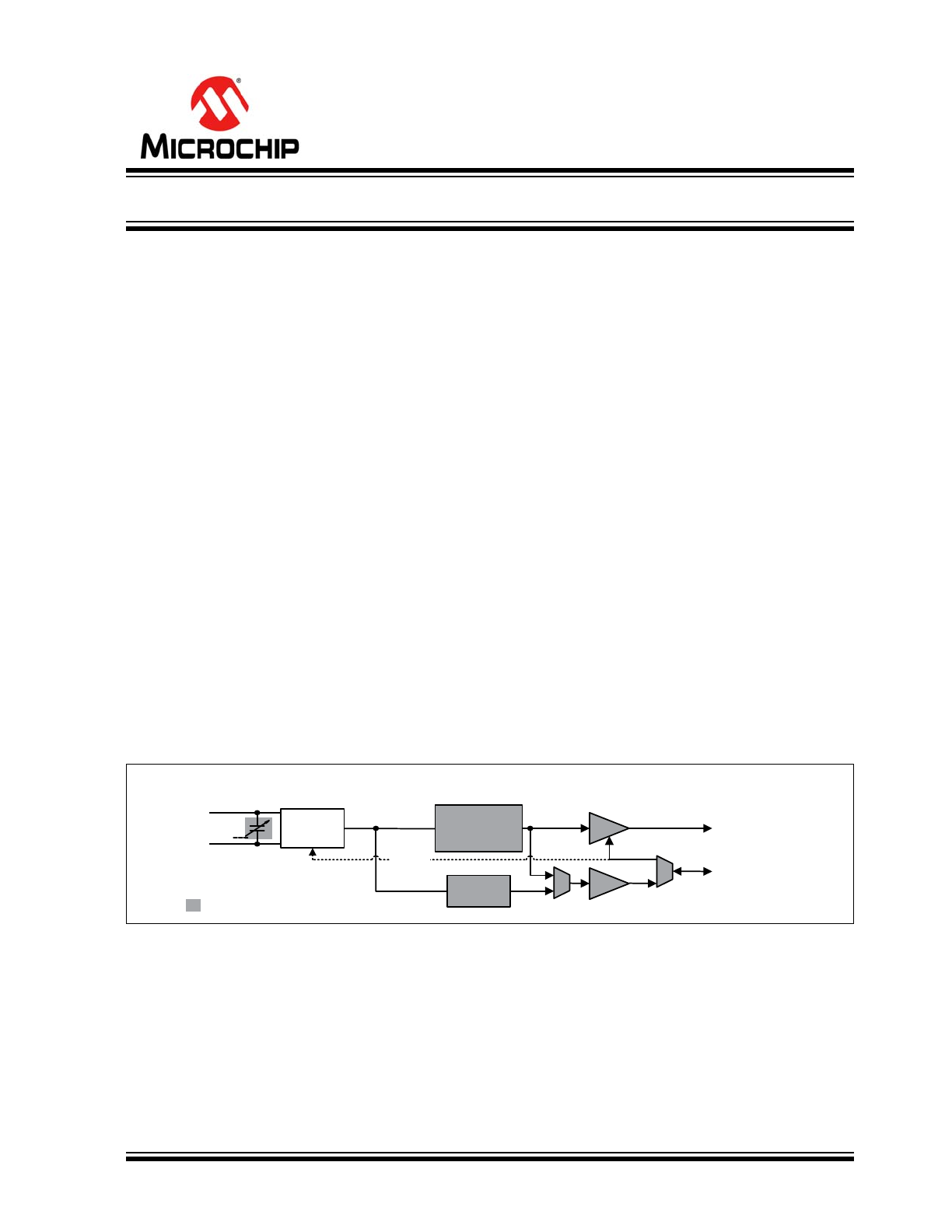
The PL610 is a high performance general purpose
oscillator IC for outputs up to 130 MHz. Designed to fit
in a small 2 mm x 1.3 mm TDFN or 3 mm x 3 mm
SOT-23 package, the PL610 offers the best phase
noise and jitter performance as well as the lowest
power consumption of any comparable IC.
In addition, there is a ‘6’ bit optional programmable
Odd/Even divider (default = ÷1), and ‘3’ programmable
output drive strengths (4 mA, 8 mA [default], 16 mA) to
choose from. The full feature set of the PL610 makes it
the most versatile XO for any application.
Block Diagram
PL610-01
FIN
XOUT
CLK0
OE, PDB, CLK1
Programmable
C
LOAD
Programmable Function
/1,
2
XTAL
OSC
P-Counter
(6-bit)
(PDB)
F
REF
1.8V to 3.3V, 1 MHz to 130 MHz XO IC

PL610-01
DS20005615A-page 2
2016 Microchip Technology Inc.
1.0
ELECTRICAL CHARACTERISTICS
Absolute Maximum Ratings †
Supply Voltage (V
DD
) ................................................................................................................................ –0.5V to +4.6V
Input Voltage (V
IN
).............................................................................................................................–0.5V to V
DD
+ 0.5V
Output Voltage (V
OUT
).......................................................................................................................–0.5V to V
DD
+ 0.5V
†
Notice: Stresses above those listed under “Absolute Maximum Ratings” may cause permanent damage to the device.
This is a stress rating only and functional operation of the device at those or any other conditions above those indicated
in the operational sections of this specification is not intended. Exposure to maximum rating conditions for extended
periods may affect device reliability. Parts are tested to commercial grade only.
2016 Microchip Technology Inc.
DS20005615A-page 3
PL610-01
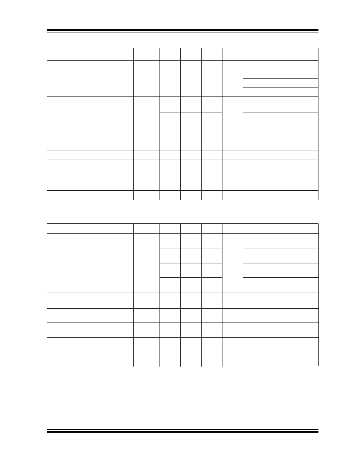
TABLE 1-1:
AC ELECTRICAL CHARACTERISTICS
Parameters
Sym.
Min.
Typ.
Max.
Units
Conditions
Crystal Input Frequency
—
5
—
130
MHz
Fundamental Crystal
FIN Input Frequency
—
1
—
130
MHz
@ V
DD
= 3.3V
@ V
DD
= 2.5V
@ V
DD
= 1.8V
FIN Input Signal Amplitude
—
0.9
—
V
DD
V
PP
Internally AC-coupled
(High Frequency)
0.1
—
V
DD
Internally AC-coupled
(Low Frequency)
3.3V <50 MHz, 2.5V <40 MHz,
1.8V <15 MHz
Output Frequency
—
0.02
—
130
MHz
@ V
DD
= 1.8V-3.3V
V
DD
Sensitivity
—
–2
—
2
ppm
Frequency vs. V
DD
±10%
Output Rise Time (see
Figure 5-1
)
—
—
1
1.2
ns
15 pF Load, 10/90% V
DD
,
High Drive, 3.3V
Output Fall Time (see
Figure 5-1
)
—
—
1
1.2
ns
15 pF Load, 10/90% V
DD
,
High Drive, 3.3V
Duty Cycle (
Note 1
, see
Figure 5-1
)
—
45
50
55
%
—
Note 1:
For 1.8V operation, the 50% ±5% duty cycle is guaranteed for frequencies ≤40 MHz.
TABLE 1-2:
DC ELECTRICAL CHARACTERISTICS
Parameters
Sym.
Min.
Typ.
Max.
Units
Conditions
Supply Current, Dynamic, with
Loaded CMOS Output
I
DD
—
3.4
—
mA
V
DD
= 3.3V, 25 MHz,
Load = 15 pF
—
2.1
—
V
DD
= 2.5V, 25 MHz,
Load = 10 pF
—
0.9
—
V
DD
= 1.8V, 25 MHz,
Load = 5 pF
—
0.65
—
V
DD
= 1.8V, 2.0 MHz,
Load = 5 pF
Operating Voltage
V
DD
1.62
—
3.63
V
—
Output Low Voltage
V
OL
—
—
0.1
V
I
OL
= +4 mA Standard Drive
Output High Voltage
V
OH
V
DD
–
0.4
—
—
V
I
OH
= –4 mA Standard Drive
Output Current, Low Drive
(See
Figure 5-2
)
I
OLD
4
—
—
mA
V
OL
= 0.4V, V
OH
= 2.4V
Output Current, Standard Drive
(See
Figure 5-2
)
I
OSD
8
—
—
mA
V
OL
= 0.4V, V
OH
= 2.4V
Output Current, High Drive
(See
Figure 5-2
)
I
OHD
16
—
—
mA
V
OL
= 0.4V, V
OH
= 2.4V
PL610-01
DS20005615A-page 4
2016 Microchip Technology Inc.
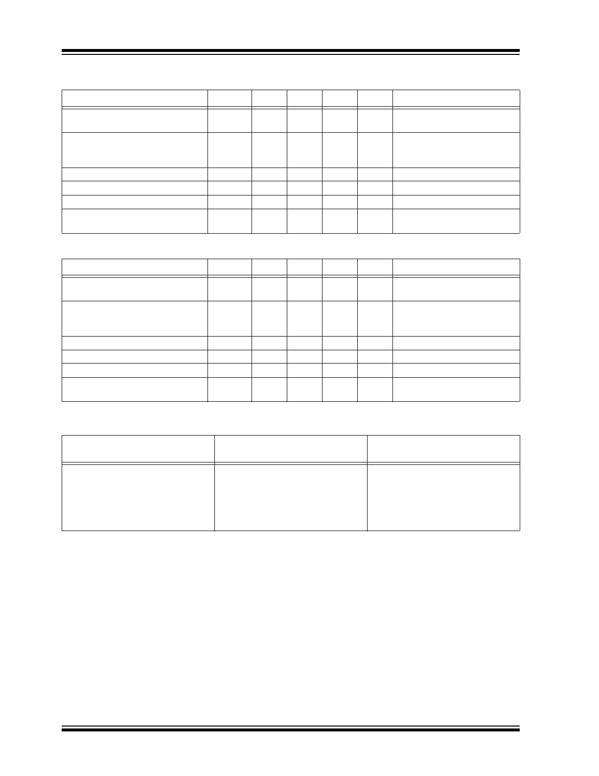
TABLE 1-3:
CRYSTAL SPECIFICATIONS (5 MHZ TO 60 MHZ)
Parameters
Sym.
Min.
Typ.
Max.
Units
Conditions
Fundamental Crystal Resonator
Frequency
F
XIN
5
—
60
MHz
—
Crystal Loading Rating
(The IC can be programmed for any
value in this range.)
C
L(XTAL)
8
—
12
pF
—
Maximum Sustainable Drive Level
—
—
—
100
µW
—
Operating Drive Level
—
—
25
—
µW
—
Crystal Shunt Capacitance
C0
—
—
3
pF
—
Effective Series Resistance,
Fundamental, (See
Figure 5-4
)
ESR
—
—
50
Ω
—
TABLE 1-4:
CRYSTAL SPECIFICATIONS (60 MHZ TO 130 MHZ)
Parameters
Sym.
Min.
Typ.
Max.
Units
Conditions
Fundamental Crystal Resonator
Frequency
F
XIN
60
—
130
MHz
—
Crystal Loading Rating
(The IC can be programmed for any
value in this range.)
C
L(XTAL)
5
—
8
pF
—
Maximum Sustainable Drive Level
—
—
—
100
µW
—
Operating Drive Level
—
—
25
—
µW
—
Crystal Shunt Capacitance
C0
—
—
2.5
pF
—
Effective Series Resistance,
Fundamental, (See
Figure 5-4
)
ESR
—
—
30
Ω
—
TABLE 1-5:
KEY PROGRAMMING PARAMETERS (OPTIONAL)
CLK[0:1]
Output Frequency
Output Drive Strength
Programmable Input/Output
F
OUT
= F
REF
÷ P*
(*: P is an Odd/Even Divider)
Where P = 6 bit
CLK0 = F
REF
, F
REF
/2 or F
REF
/P
CLK1 = F
REF
, F
REF
/2 or CLK0
Three optional drive strengths to
choose from:
• Low: 4 mA
• Std: 8 mA (default)
• High: 16 mA
One output pin can be configured
as:
• OE - input
• PDB - input
• CLK1 – output
2016 Microchip Technology Inc.
DS20005615A-page 5
PL610-01
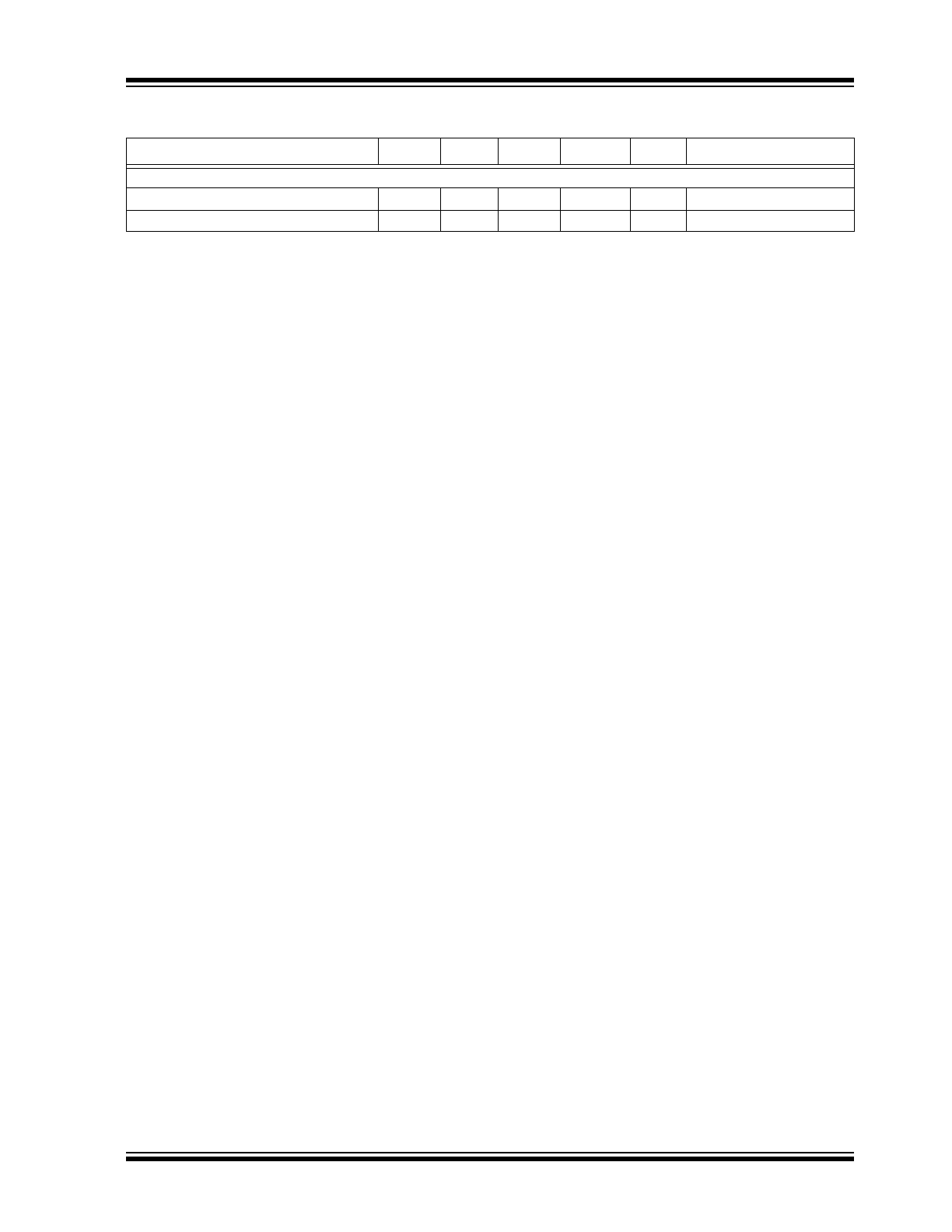
TEMPERATURE SPECIFICATIONS (
Note 1
)
Parameters
Sym.
Min.
Typ.
Max.
Units
Conditions
Temperature Ranges
Storage Temperature Range
T
S
–65
—
+150
°C
—
Ambient Operating Temperature
T
A
–40
—
+85
°C
—
Note 1:
Exposure of the device under conditions beyond the limits specified by the maximum ratings for extended
periods may cause permanent damage to the device and affect product reliability. These conditions
represent a stress rating only, and functional operations of the device at these or any other conditions
above the operational limits noted in this specification is not implied. Operating temperature is guaranteed
by design. Parts are tested to commercial grade only.
PL610-01
DS20005615A-page 6
2016 Microchip Technology Inc.
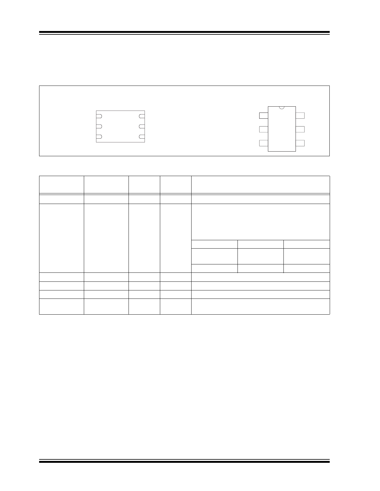
2.0
PIN DESCRIPTIONS
The descriptions of the pins are listed in
Table 2-1
.
Pin Configurations
TABLE 2-1:
PIN FUNCTION TABLE
6-Pin TDFN
Pin Number
6-Pin SOT-23
Pin Number
Name
Type
Description
1
3
XIN, FIN
I
Crystal or Reference Clock input pin
2
1
OE, PDB,
CLK1
I/O
This programmable I/O pin can be configured as an
Output Enable (OE) input, Power Down input (PDB)
input or CLK1 clock output. This pin has an internal
60 kΩ pull-up resistor for OE and 10 MΩ pull up
resistor for PDB.
State
OE
PDB
0
Tri-State CLK
Power Down
Mode
1 (default)
Normal Mode
Normal Mode
3
2
GND
P
GND connection
4
6
CLK0
O
Programmable Clock Output
5
5
VDD
P
V
DD
connection
6
4
XOUT
O
Crystal Output pin. Do Not Connect (DNC) when FIN is
present.
PL610-01
6-Pin TDFN
XIN, FIN
GND
XOUT
VDD
CLK0
OE^, PDB^, CLK1
1
4
5
6
3
2
1
2
3
4
5
6
OE^, PDB^, CLK1
GND
XIN, FIN
VDD
XOUT
CLK0
PL610-01
6-Pin SOT-23

2016 Microchip Technology Inc.
DS20005615A-page 7
PL610-01
3.0
FUNCTIONAL DESCRIPTION
PL610-01 is a highly featured, very flexible, advanced
XO design for high performance, low-power, small
form-factor applications. The PL610-01 accepts a
fundamental input crystal of 5 MHz to 130 MHz or a
reference clock input of 1 MHz to 130 MHz and is
capable of producing two outputs up to 130 MHz. This
flexible design allows the PL610-01 to deliver any
frequency, F
REF
(Crystal or Ref Clk) frequency, F
REF
/2
or F
REF
/P to CLK0 and/or CLK1. Some of the design
features of the PL610-01 are mentioned below.
3.1
Clock Output (CLK0)
CLK0 is the main clock output. The output from CLK0
can be F
REF
(Crystal or Ref Clk), F
REF
/2 or F
REF
/P
output. The output drive level can be programmed to
Low Drive (4 mA), Standard Drive (8 mA), or High Drive
(16 mA).
3.2
Programmable I/O (OE/PDB/CLK1)
The PL610-01 provides one programmable I/O pin
which can be configured as one of the following
functions:
3.2.1
OUTPUT ENABLE (OE)
The Output Enable feature allows the user to enable
and disable the clock output(s) by toggling the OE pin.
The OE pin incorporates a 60 kΩ pull-up resistor giving
a default condition of logic “1”.
3.2.2
POWER DOWN CONTROL (PDB)
The Power Down (PDB) feature allows the user to put
the PL610-01 into “Sleep Mode.” When activated (logic
‘0’), PDB disables the PLL, the oscillator circuitry,
counters, and all other active circuitry. In Power Down
mode the IC consumes <10 µA of power. The PDB pin
incorporates a 10 MΩ pull-up resistor giving a default
condition of logic “1”.
3.2.3
CLOCK OUTPUT (CLK1)
The CLK1 feature allows the PL610-01 to have an
additional clock output programmed to one of the
following:
• F
REF
- Reference (Crystal or Ref Clk) Frequency
• F
REF
/2
• CLK0
PL610-01
DS20005615A-page 8
2016 Microchip Technology Inc.
4.0
LAYOUT RECOMMENDATIONS
The following guidelines are to assist you with a
performance-optimized PCB design.
4.1
Signal Integrity and Termination
Considerations
• Keep traces short.
• Trace = Inductor. With a capacitive load this
creates ringing.
• Long trace = Transmission Line. Without proper
termination this will cause reflections (looks like
ringing).
• Design long traces as “striplines” or “microstrips”
with defined impedance.
• Match trace at one side to avoid reflections
bouncing back and forth.
4.2
Decoupling and Power Supply
Considerations
• Place decoupling capacitors as close as possible
to the V
DD
pin(s) to limit noise from the power
supply.
• Multiple V
DD
pins should be decoupled separately
for best performance.
• Addition of a ferrite bead in series with V
DD
can
help prevent noise from other board sources.
• Value of decoupling capacitor is frequency
dependent. Typical values to use are 0.1 µF for
designs using crystals <50 MHz and 0.01 µF for
designs using crystals >50 MHz.
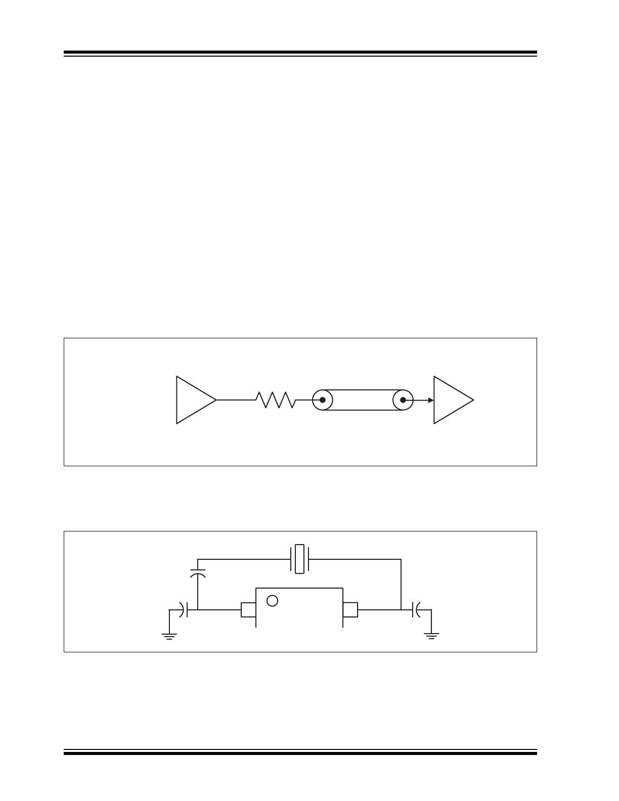
4.3
Typical CMOS Termination
Place series resistor as close as possible to the CMOS output.
FIGURE 4-1:
Typical CMOS Termination.
4.4
Crystal Tuning Circuit
Series and parallel capacitors are used to fine tune the crystal load to the circuit load.
CST:
Series capacitor, used to lower circuit load to match crystal load. Raises frequency offset. This can be eliminated
by using a crystal with a C
LOAD
of equal or greater value than the oscillator.
CPT:
Parallel capacitors, used to raise the circuit load to match the crystal load. Lowers frequency offset.
CMOS Output Buffer
(Typical buffer impedance 20
:
To CMOS Input
Series Resistor
Use value to match output
buffer impedance to 50
:
trace. Typical value 30
:
50
: line
XIN
XOUT
Cpt
Cpt
Cst
2016 Microchip Technology Inc.
DS20005615A-page 9
PL610-01
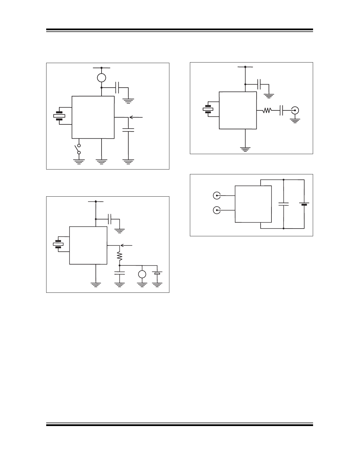
5.0
MEASUREMENT TEST
CIRCUITS (MTC)
FIGURE 5-1:
MTC-1: Rise Time, Fall
Time, Duty Cycle, V
OL
, V
OH
, I
DD
, Power Down
Current, Output Enable/Disable.
FIGURE 5-2:
MTC-2: Output Drive
Current and Output Impedance.
FIGURE 5-3:
MTC-3: Jitter and Phase
Noise.
FIGURE 5-4:
MTC-4 Negative
Resistance.
XIN
VDD
XOUT
GND
CLK
OE^
FET
Probe
CL
A
0.1μF
XOUT
XIN
OE^
Probe
FET
CLK
VDD
GND
0.1μF
0.1μF
V
R
XOUT
OE^
GND
0.1μF
XIN
CLK
VDD
0.1μF
XIN
OE^
XOUT
CLK
GND
VDD
0.1μF
Network
Analyzer
PL610-01
DS20005615A-page 10
2016 Microchip Technology Inc.
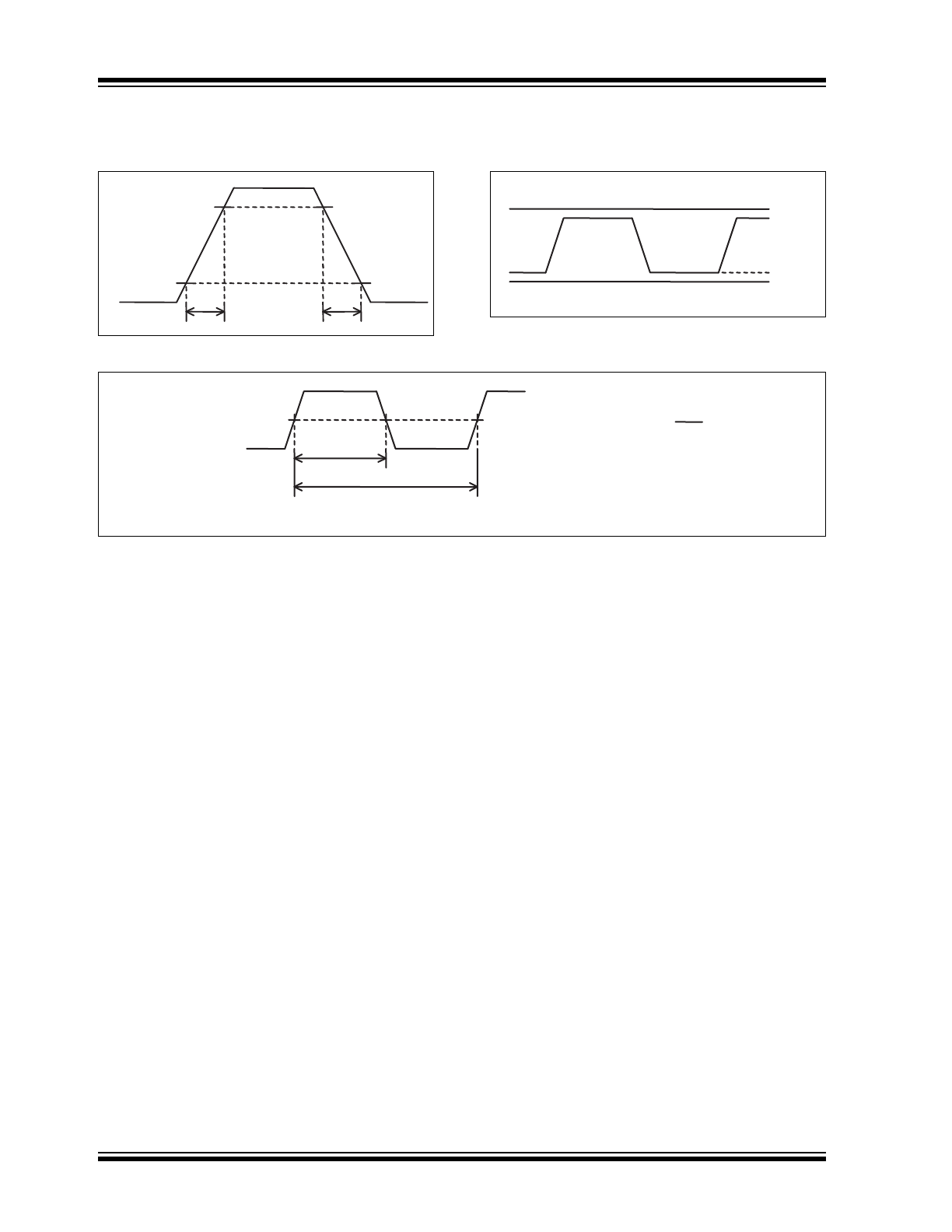
6.0
WAVEFORM SWITCHING
CHARACTERISTICS
FIGURE 6-1:
Rise and Fall Times.
FIGURE 6-2:
V
OH
, V
OL
.
FIGURE 6-3:
Duty Cycle.
tr
tf
10%VDD
90%VDD
GND
VDD
VOH
VOL
50%VDD
Tw
T
Duty Cycle = 100% ×
Tw
T