
© 2007 Microchip Technology Inc.
DS21424D-page 1
TC4431/TC4432
Features
• High Peak Output Current – 1.5 A
• Wide Input Supply Operating Range:
- 4.5V to 30V
• High Capacitive Load Drive Capability:
- 1000 pF in 25 nsec
• Short Delay Times – <78 nsec Typ.
• Low Supply Current:
- With Logic ‘1’ Input – 2.5 mA
- With Logic ‘0’ Input – 300 µA
• Low Output Impedance – 7
Ω
• Latch-Up Protected: Will Withstand >300 mA
Reverse Current
• ESD Protected – 4 kV
Applications
• Small Motor Drive
• Power MOSFET Driver
• Driving Bipolar Transistors
General Description
The TC4431/TC4432 are 30V CMOS buffer/drivers
suitable for use in high-side driver applications. They
will not latch up under any conditions within their power
and voltage ratings. They can accept, without damage
or logic upset, up to 300 mA of reverse current (of
either polarity) being forced back into their outputs. All
terminals are fully protected against up to 4 kV of
electrostatic discharge.
Under-voltage lockout circuitry forces the output to a
‘low’ state when the input supply voltage drops below
7V. For operation at lower voltages, disable the lockout
and start-up circuit by grounding pin 3 (LOCK DIS); for
all other situations, pin 3 (LOCK DIS) should be left
floating. The under-voltage lockout and start-up circuit
gives brown out protection when driving MOSFETS.
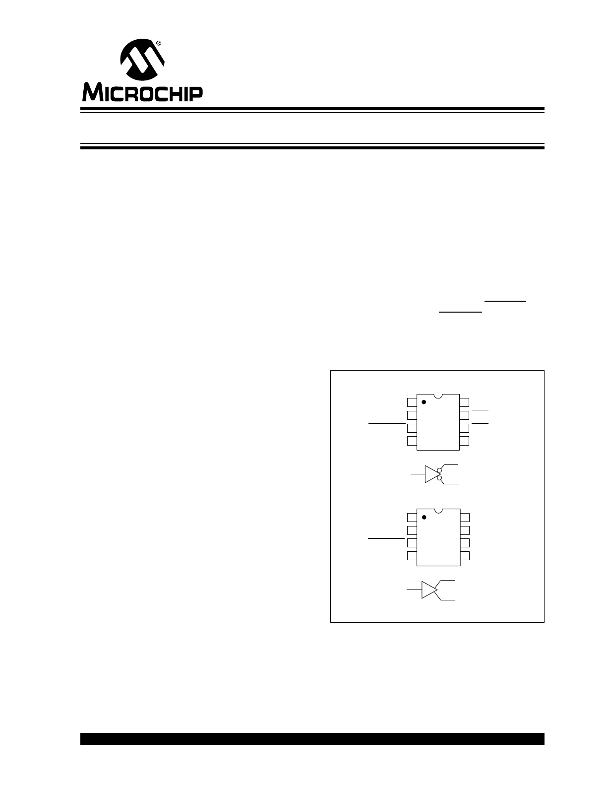
Package Type
OUT
TC4431
1
2
3
4
V
DD
5
6
7
8
OUT
GND
V
DD
IN
LOCK DIS
GND
TC4432
1
2
3
4
V
DD
5
6
7
8
OUT
GND
V
DD
IN
GND
2
7
Inverting
Non Inverting
OUT
6
LOCK DIS
2
7
6
8-Pin PDIP/SOIC/CERDIP
1.5A High-Speed 30V MOSFET Drivers
TC4431/TC4432
DS21424D-page 2
© 2007 Microchip Technology Inc.
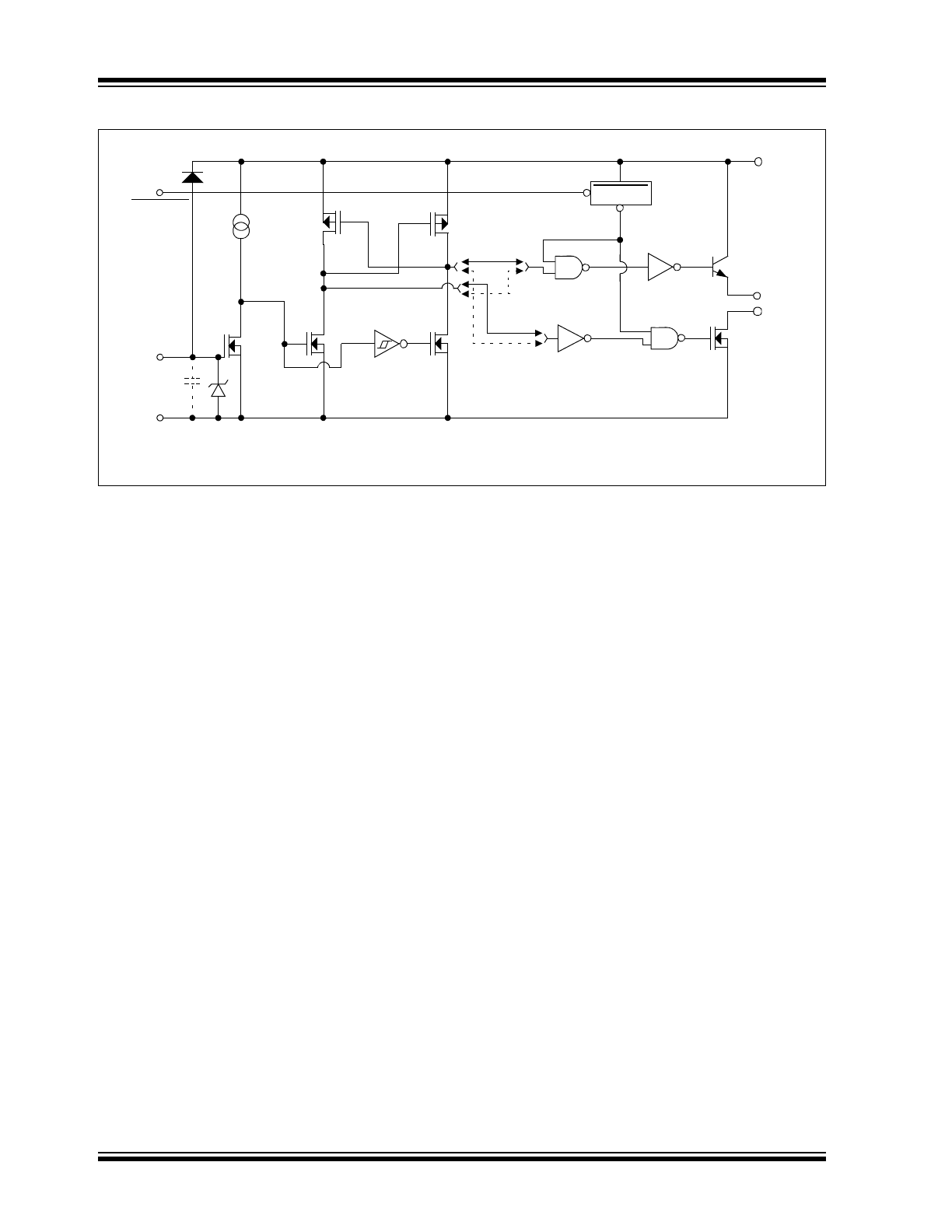
Functional Block Diagram
2 mA
OUT
Input
GND
Effective
Input
C = 10 pF
VDD
TC4431/TC4432
Inverting/Non Inverting
OUT
UV LOCK
Inverting
TC4431
250 mV
LOCK DIS
3
2
4, 5
Non Inverting
TC4432
6
7
8
© 2007 Microchip Technology Inc.
DS21424D-page 3
TC4431/TC4432
1.0
ELECTRICAL
CHARACTERISTICS
Absolute Maximum Ratings†
Supply Voltage ....................................................... 36V
Input Voltage (Note 1)................... V
DD
+ 0.3V to GND
Package Power Dissipation (T
A
≤ 70°C)
PDIP ............................................................ 730 mW
CERDIP ....................................................... 800 mW
SOIC............................................................ 470 mW
Maximum Junction Temperature, T
J
................ +150°C
Storage Temperature Range .............. -65°C to +150°C
† Stresses above those listed under "Absolute Maximum
Ratings" may cause permanent damage to the device. These
are stress ratings only and functional operation of the device
at these or any other conditions above those indicated in the
operation sections of the specifications is not implied.
Exposure to Absolute Maximum Rating conditions for
extended periods may affect device reliability.
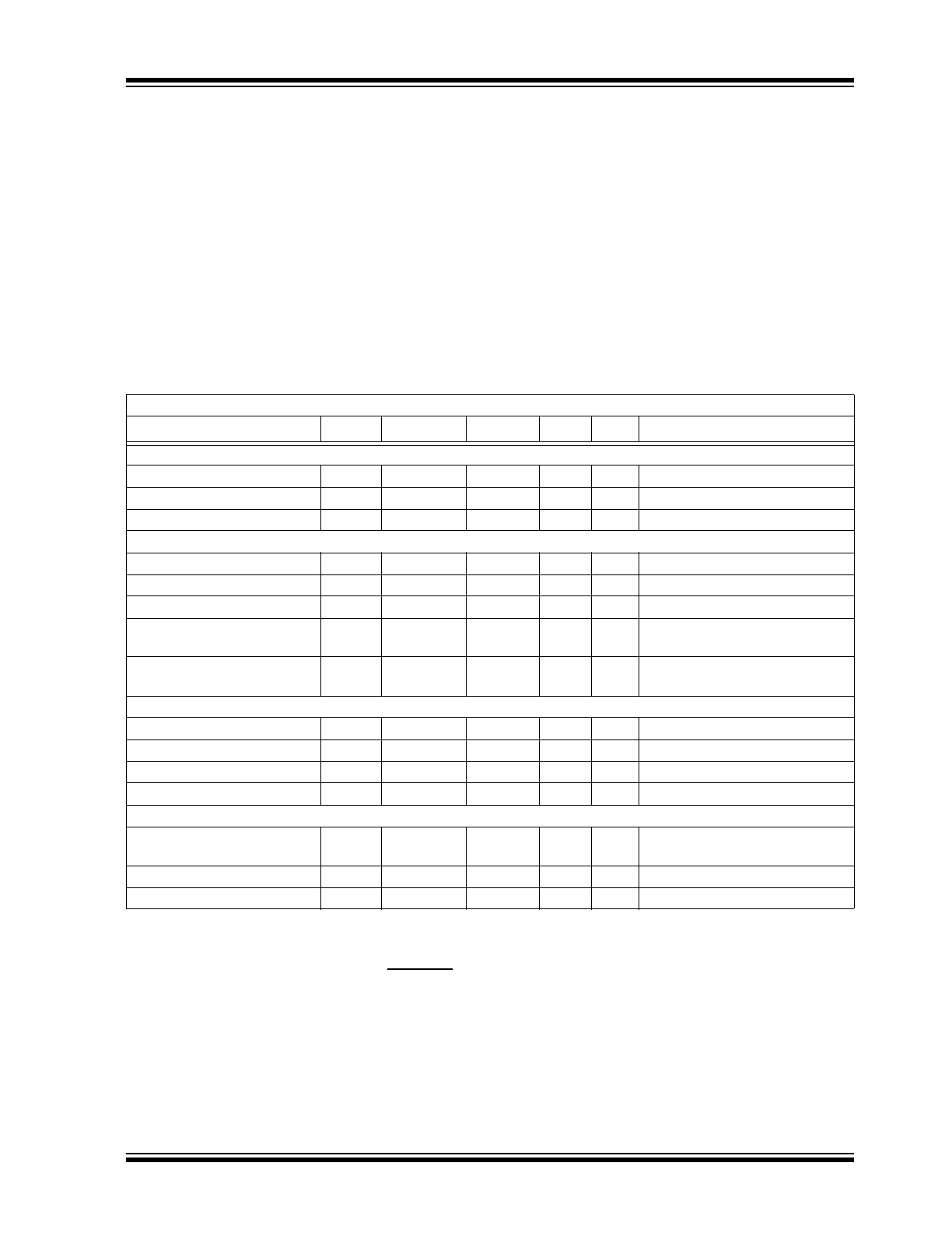
DC CHARACTERISTICS
Electrical Specifications: Unless otherwise noted, T
A
= +25ºC with 4.5V
≤ V
DD
≤ 30V.
Parameters
Sym
Min
Typ
Max
Units
Conditions
Input
Logic ‘1’, High Input Voltage
V
IH
2.4
—
—
V
Logic ‘0’, Low Input Voltage
V
IL
—
—
0.8
V
Input Current (Note 1)
I
IN
-1
—
1
µA
0V
≤ V
IN
≤ 12V
Output
High Output Voltage
V
OH
V
DD
– 1.0
V
DD
– 0.8
—
V
I
OUT
= 100 mA
Low Output Voltage
V
OL
—
—
0.025
V
Output Resistance
R
O
—
7
10
Ω
I
OUT
= 10 mA, V
DD
= 30V
Peak Output Current
I
PK
—
—
3.0
1.5
—
—
A
Source: V
DD
= 30V
Sink: V
DD
= 30V
Latch-Up Protection
Withstand Reverse Current
I
REV
—
0.3
—
A
Duty cycle
≤ 2%, t ≤ 300 µsec
Switching Time (Note 2)
Rise Time
t
R
—
25
40
ns
Figure 4-1
Fall Time
t
F
—
33
50
ns
Figure 4-1
Delay Time
t
D1
—
62
80
ns
Figure 4-1
Delay Time
t
D2
—
78
90
ns
Figure 4-1
Power Supply
Power Supply Current
I
S
—
—
2.5
0.3
4
0.4
mA
V
IN
= 3V
V
IN
= 0V
Start-up Threshold
V
S
—
8.4
10
V
Drop-out Threshold
V
DO
7
7.7
—
V
Note 3
Note 1:
For inputs >12V, add a 1 k
Ω resistor in series with the input. See Section 2.0 “Typical Performance
Curves” for input current graph.
2:
Switching times are ensured by design.
3:
For operation below 7V, pin 3 (LOCK DIS) should be tied to ground to disable the lockout and start-up
circuit, otherwise, pin 3 must be left floating.
TC4431/TC4432
DS21424D-page 4
© 2007 Microchip Technology Inc.
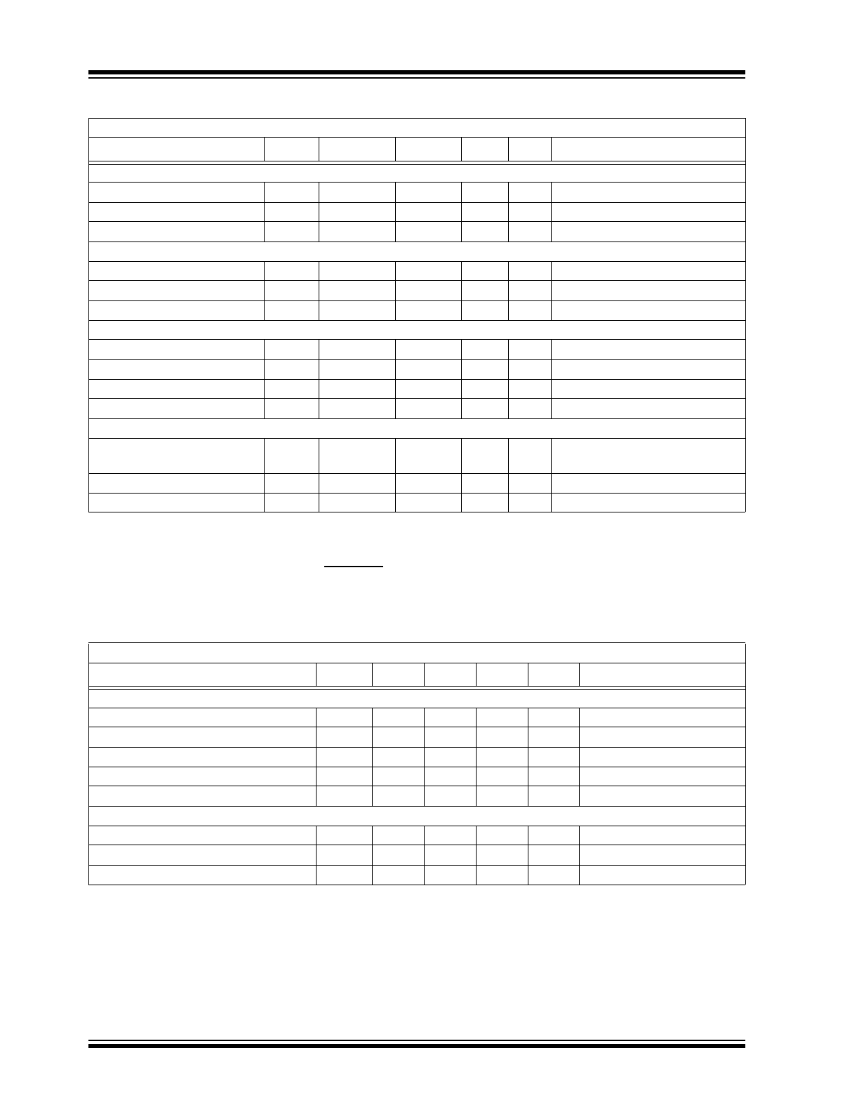
DC CHARACTERISTICS
TEMPERATURE CHARACTERISTICS
Electrical Specifications: Unless otherwise noted, Over operating temperature range with 4.5V
≤ V
DD
≤ 30V.
Parameters
Sym
Min
Typ
Max
Units
Conditions
Input
Logic ‘1’, High Input Voltage
V
IH
2.4
—
—
V
Logic ‘0’, Low Input Voltage
V
IL
—
—
0.8
V
Input Current (Note 1)
I
IN
-10
—
10
µA
0V
≤ V
IN
≤ 12V
Output
High Output Voltage
V
OH
V
DD
– 1.2
—
—
V
I
OUT
= 100 mA
Low Output Voltage
V
OL
—
—
0.025
V
Output Resistance
R
O
—
—
12
Ω
I
OUT
= 10 mA, V
DD
= 30V
Switching Time (Note 2)
Rise Time
t
R
—
—
60
ns
Figure 4-1
Fall Time
t
F
—
—
70
ns
Figure 4-1
Delay Time
t
D1
—
—
100
ns
Figure 4-1
Delay Time
t
D2
—
—
110
ns
Figure 4-1
Power Supply
Power Supply Current
I
S
—
—
—
—
6
0.7
mA
V
IN
= 3V
V
IN
= 0V
Start-up Threshold
V
S
—
8.4
10
V
Drop-out Threshold
V
DO
7
7.7
—
V
Note 3
Note 1:
For inputs >12V, add a 1 k
Ω resistor in series with the input. See Section 2.0 “Typical Performance
Curves” for input current graph.
2:
Switching times are ensured by design.
3:
For operation below 7V, pin 3 (LOCK DIS) should be tied to ground to disable the lockout and start-up cir-
cuit, otherwise, pin 3 must be left floating.
Electrical Specifications: Unless otherwise noted, all parameters apply with 4.5V
≤ V
DD
≤ 30V.
Parameters
Sym
Min
Typ
Max
Units
Conditions
Temperature Ranges
Specified Temperature Range (C)
T
A
0
—
+70
ºC
Specified Temperature Range (E)
T
A
-40
—
+85
ºC
Specified Temperature Range (V)
T
A
-40
—
+125
ºC
Maximum Junction Temperature
T
J
—
—
+150
ºC
Storage Temperature Range
T
A
-65
—
+150
ºC
Package Thermal Resistances:
Thermal Resistance, 8L-SOIC
θ
JA
—
155
—
ºC/W
Thermal Resistance, 8L-PDIP
θ
JA
—
125
—
ºC/W
Thermal Resistance, 8L-CERDIP
θ
JA
—
150
—
ºC/W
© 2007 Microchip Technology Inc.
DS21424D-page 5
TC4431/TC4432
2.0
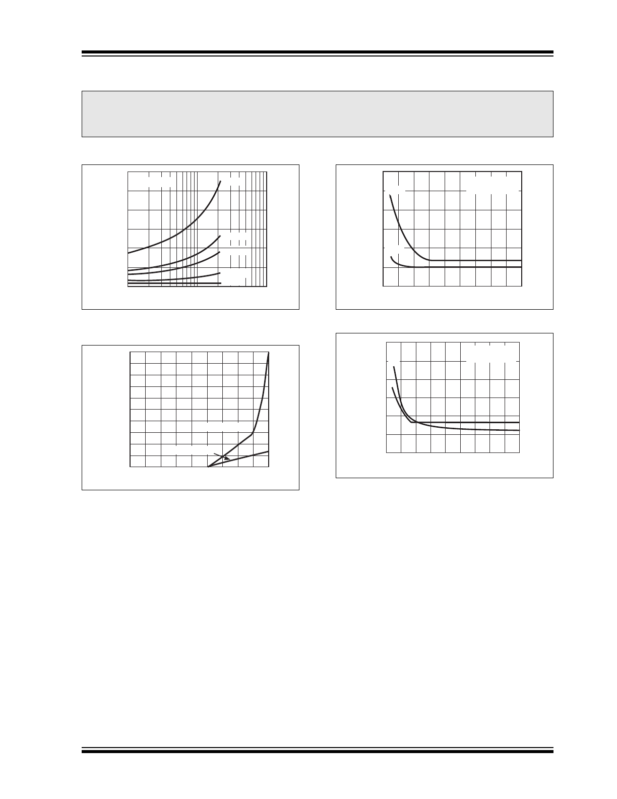
TYPICAL PERFORMANCE CURVES
Note: Unless otherwise indicated, T
A
= +25ºC with 4.5V
≤ V
DD
≤ 30V.
FIGURE 2-1:
Supply Current vs.
Capacitive Load.
FIGURE 2-2:
Input Current vs. Input
Voltage.
FIGURE 2-3:
Rise/Fall Time vs. V
DD
.
FIGURE 2-4:
t
D1
and t
D2
Delay vs. V
DD
.
Note:
The graphs and tables provided following this note are a statistical summary based on a limited number of
samples and are provided for informational purposes only. The performance characteristics listed herein
are not tested or guaranteed. In some graphs or tables, the data presented may be outside the specified
operating range (e.g., outside specified power supply range) and therefore outside the warranted range.
100
1000
10,000
2 MHz
600 kHz
200 kHz
20 kHz
900 kHz
V = 12V
DD
60
50
40
30
20
10
0
I
SUPPLY
(mA)
C
LOAD
(pF)
INPUT CURRENT (mA)
INPUT VOLTAGE (V
IN
)
50
3
6
12
15
18
21
24
27
30
9
40
30
20
10
0
WITHOUT 1 K RES.
45
35
25
15
5
WITH 1 K RES.
Time (nsec)
3
6
12
15
18
21
24
27
30
9
150
125
100
75
50
25
0
t
FALL
V
DD
(V)
C
LOAD
= 1000 pF
T
A
= +25°C
t
RISE
TIME (nsec)
3
6
12
15
18
21
24
27
30
9
300
250
200
150
100
50
0
tD2
tD1
C
LOAD
= 1000 pF
T
A
= +25°C
V
DD
(V)
TC4431/TC4432
DS21424D-page 6
© 2007 Microchip Technology Inc.
3.0
PIN DESCRIPTIONS
The descriptions of the pins are listed in
Table 3-1
.
TABLE 3-1:
PIN FUNCTION TABLE
3.1
Supply Input (V
DD
)
The V
DD
input is the bias supply input for the MOSFET
driver and is rated for 4.5V to 30V with respect to the
ground pins. The V
DD
input should be bypassed to
ground with a local ceramic capacitor. The value of this
capacitor should be chosen based on the capacitive
load that is being driven.
3.2
Control Input (IN)
The MOSFET driver input is a TTL/CMOS compatible
input with 250 mV of hysteresis between the high and
low threshold voltages. If an input signal level of greater
than 12V is applied to the device, a series current
limiting resistor is recommended.
3.3
Lockout Disable (LOCK DIS)
The lockout pin enables/disables the undervoltage
lockout feature of the device. If undervoltage lockout is
desired (output is not enabled until the bias voltage
reaches 8.4V (typical) on the rising edge and is
disabled when the bias voltage reaches 7.7V (typical)
on the falling edge), the lockout pin should be left float-
ing. If operation below 7V is desired, the lockout pin
should be tied to ground.
3.4
Ground (GND)
The ground pins are the return path for the bias current
and for the high peak currents which discharge the load
capacitor. Both ground pins should be used to ensure
proper operation. The ground pins should be tied into a
ground plane or have short traces to the bias supply
source return.
3.5
Drive Output (OUT)
The TC4431/TC4432 devices have individual source
and sink output pins. This feature can be used to adjust
the rise and fall time independently by adding separate
charge and discharge resistors external to the device.
Pin 7 (source output) can source 3 A peak currents into
capacitive loads and pin 6 (sink output) can sink 1.5 A
peak currents from a capacitive load.
Pin No.
Symbol
Description
1
V
DD
Supply Input, 4.5V to 30V
2
IN
TTL/CMOS Compatible Input
3
LOCK DIS
Input Pin, Enable/Disable for UV Lockout
4
GND
Ground
5
GND
Ground
6
OUT
Drive Output, Pull Down
7
OUT
Drive Output, Pull Up
8
V
DD
Supply Input, 4.5V to 30V
© 2007 Microchip Technology Inc.
DS21424D-page 7
TC4431/TC4432
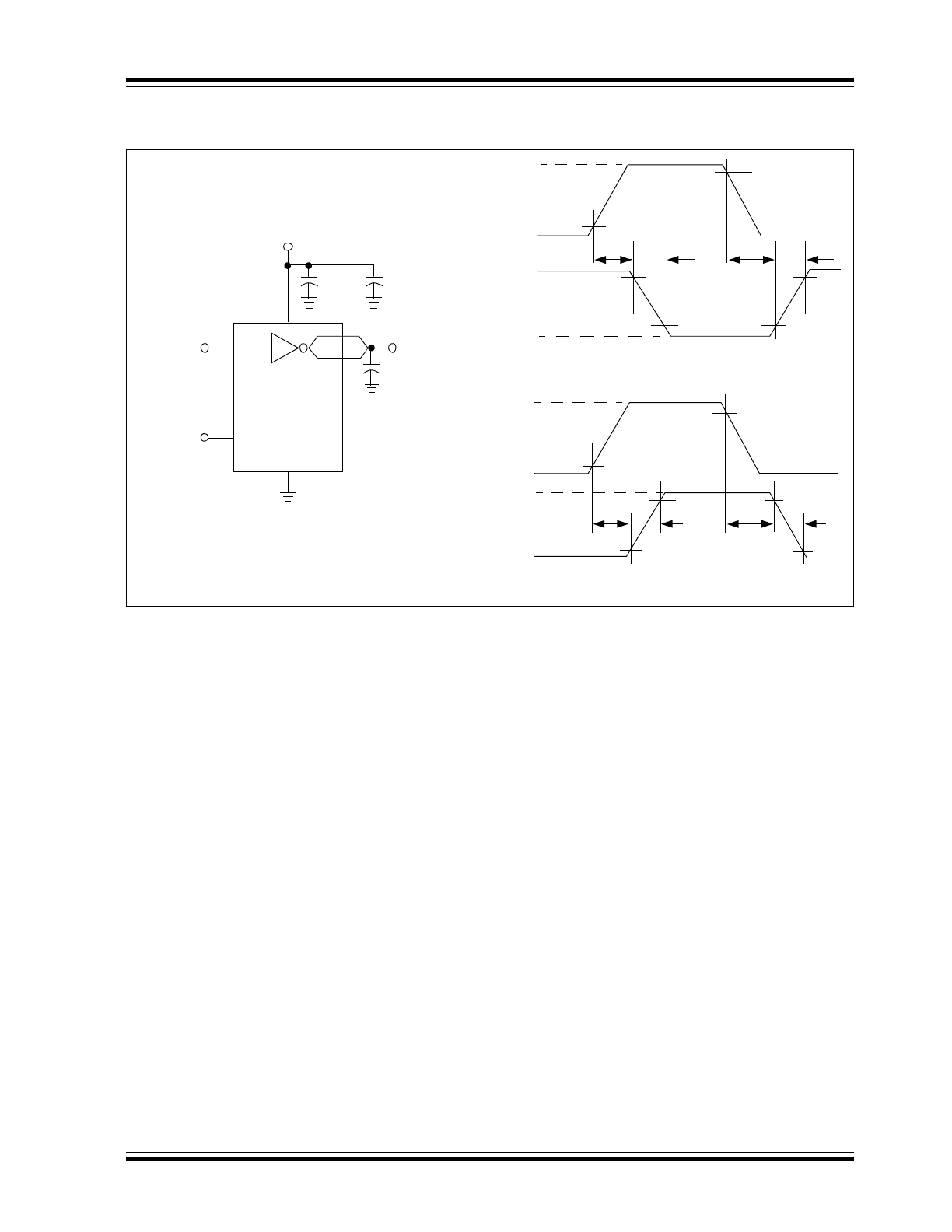
4.0
APPLICATIONS INFORMATION
FIGURE 4-1:
Switching Time Test Circuit.
CL = 1000 pF
0.1 µF
4.7 µF
Inverting Driver
Non Inverting Driver
Input
V
DD
= 30V
Input
Output
t
D1
t
F
t
R
t
D2
Input: 100 kHz,
square wave,
t
RISE
= t
FALL
≤ 10 nsec
Output
Input
Output
t
D1
t
F
t
R
t
D2
+5V
10%
90%
10%
90%
10%
90%
V
DD
0V
90%
10%
10%
10%
90%
+5V
V
DD
0V
0V
0V
90%
4, 5
2
6
1, 8
LOCK DIS
3
7
TC4431/TC4432
DS21424D-page 8
© 2007 Microchip Technology Inc.
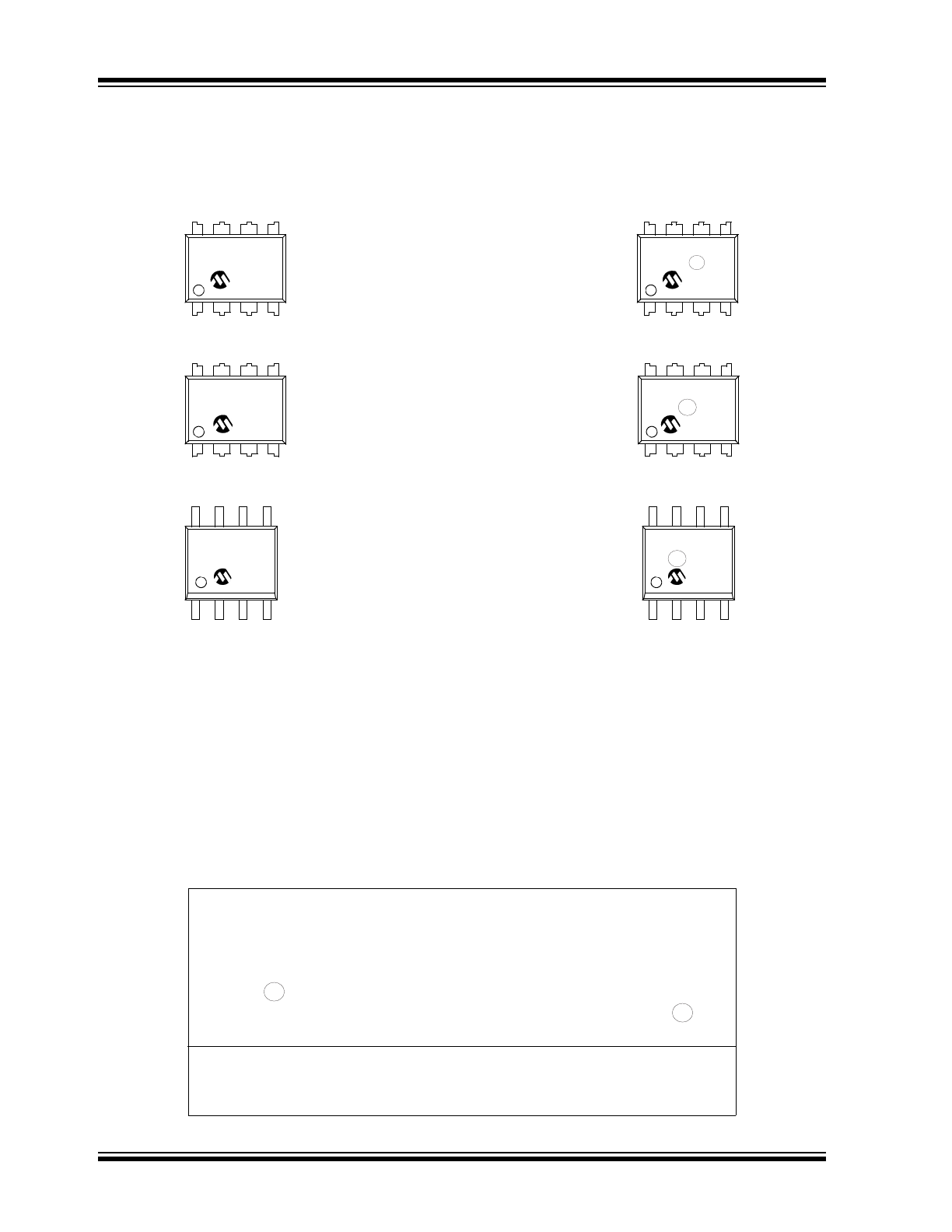
5.0
PACKAGING INFORMATION
5.1
Package Marking Information
XXXXXXXX
XXXXXNNN
YYWW
8-Lead PDIP (300 mil)
Example:
8-Lead SOIC (150 mil)
Example:
XXXXXXXX
XXXXYYWW
NNN
TC4431
EPA^^256
0749
TC4431E
OA^^0749
256
8-Lead CERDIP (300 mil)
Example:
XXXXXXXX
XXXXXNNN
YYWW
TC4432
EJA^^256
0749
Legend: XX...X
Customer-specific information
Y
Year code (last digit of calendar year)
YY
Year code (last 2 digits of calendar year)
WW
Week code (week of January 1 is week ‘01’)
NNN
Alphanumeric traceability code
Pb-free JEDEC designator for Matte Tin (Sn)
*
This package is Pb-free. The Pb-free JEDEC designator ( )
can be found on the outer packaging for this package.
Note:
In the event the full Microchip part number cannot be marked on one line, it will
be carried over to the next line, thus limiting the number of available
characters for customer-specific information.
3
e
3
e
3
e
3
e
3
e
© 2007 Microchip Technology Inc.
DS21424D-page 9
TC4431/TC4432
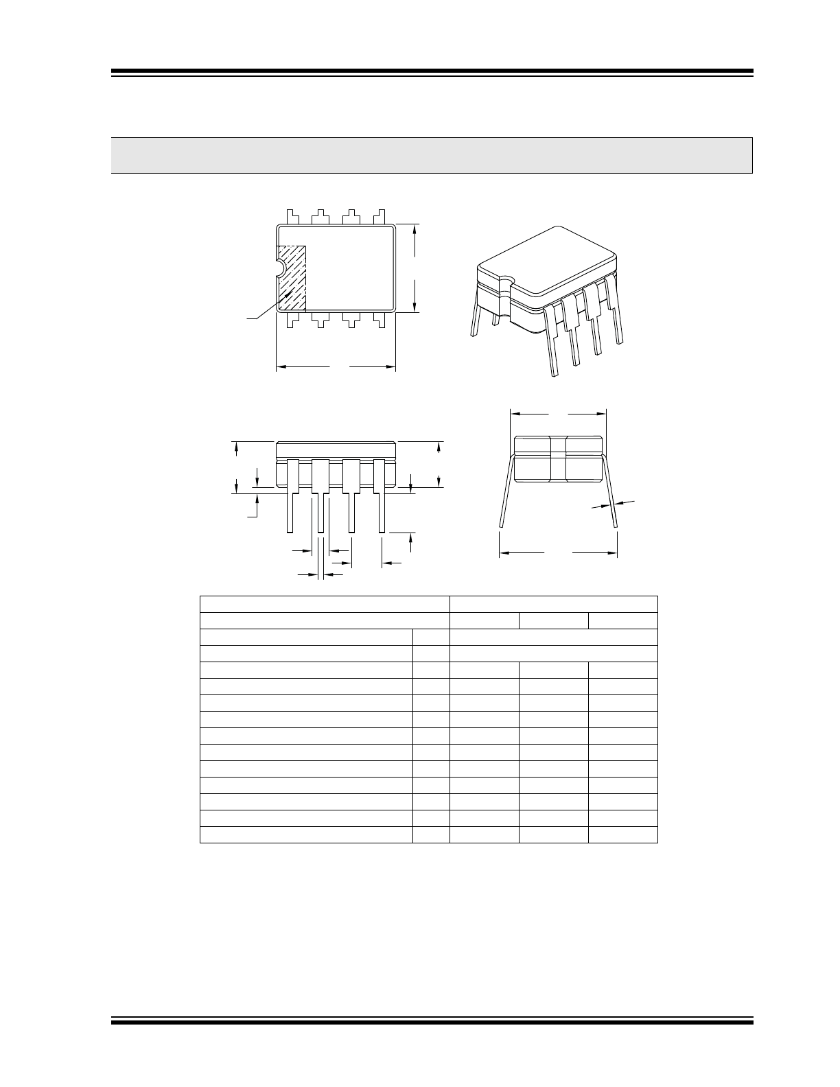
/HDG&HUDPLF'XDO,Q/LQH-$±%RG\>&(5',3@
1RWHV
3LQYLVXDOLQGH[IHDWXUHPD\YDU\EXWPXVWEHORFDWHGZLWKLQWKHKDWFKHGDUHD
6LJQLILFDQW&KDUDFWHULVWLF
'LPHQVLRQLQJDQGWROHUDQFLQJSHU$60(<0
%6& %DVLF'LPHQVLRQ7KHRUHWLFDOO\H[DFWYDOXHVKRZQZLWKRXWWROHUDQFHV
1RWH
)RUWKHPRVWFXUUHQWSDFNDJHGUDZLQJVSOHDVHVHHWKH0LFURFKLS3DFNDJLQJ6SHFLILFDWLRQORFDWHGDW
KWWSZZZPLFURFKLSFRPSDFNDJLQJ
8QLWV
,1&+(6
'LPHQVLRQ/LPLWV
0,1
120
0$;
1XPEHURI3LQV
1
3LWFK
H
%6&
7RSWR6HDWLQJ3ODQH
$
±
±
6WDQGRII
$
±
±
&HUDPLF3DFNDJH+HLJKW
$
±
6KRXOGHUWR6KRXOGHU:LGWK
(
±
&HUDPLF3DFNDJH:LGWK
(
2YHUDOO/HQJWK
'
7LSWR6HDWLQJ3ODQH
/
±
/HDG7KLFNQHVV
F
±
8SSHU/HDG:LGWK
E
±
/RZHU/HDG:LGWK
E
±
2YHUDOO5RZ6SDFLQJ
(
±
N
NOTE 1
E1
1
2
D
E
c
E2
A2
L
e
b
b1
A1
A
0LFURFKLS 7HFKQRORJ\ 'UDZLQJ &%
TC4431/TC4432
DS21424D-page 10
© 2007 Microchip Technology Inc.
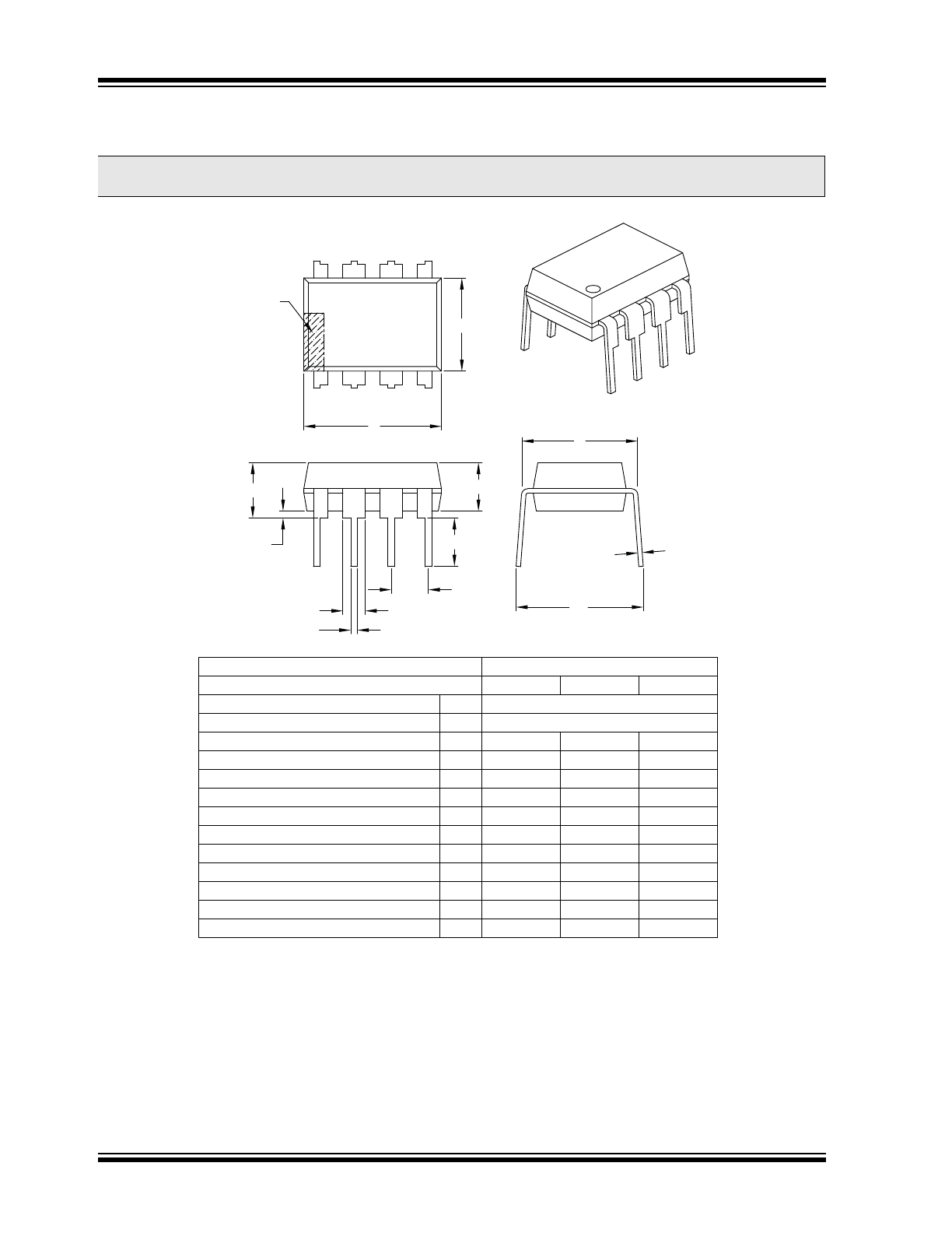
/HDG3ODVWLF'XDO,Q/LQH3±PLO%RG\>3',3@
1RWHV
3LQYLVXDOLQGH[IHDWXUHPD\YDU\EXWPXVWEHORFDWHGZLWKWKHKDWFKHGDUHD
6LJQLILFDQW&KDUDFWHULVWLF
'LPHQVLRQV'DQG(GRQRWLQFOXGHPROGIODVKRUSURWUXVLRQV0ROGIODVKRUSURWUXVLRQVVKDOOQRWH[FHHGSHUVLGH
'LPHQVLRQLQJDQGWROHUDQFLQJSHU$60(<0
%6&%DVLF'LPHQVLRQ7KHRUHWLFDOO\H[DFWYDOXHVKRZQZLWKRXWWROHUDQFHV
1RWH
)RUWKHPRVWFXUUHQWSDFNDJHGUDZLQJVSOHDVHVHHWKH0LFURFKLS3DFNDJLQJ6SHFLILFDWLRQORFDWHGDW
KWWSZZZPLFURFKLSFRPSDFNDJLQJ
8QLWV
,1&+(6
'LPHQVLRQ/LPLWV
0,1
120
0$;
1XPEHURI3LQV
1
3LWFK
H
%6&
7RSWR6HDWLQJ3ODQH
$
±
±
0ROGHG3DFNDJH7KLFNQHVV
$
%DVHWR6HDWLQJ3ODQH
$
±
±
6KRXOGHUWR6KRXOGHU:LGWK
(
0ROGHG3DFNDJH:LGWK
(
2YHUDOO/HQJWK
'
7LSWR6HDWLQJ3ODQH
/
/HDG7KLFNQHVV
F
8SSHU/HDG:LGWK
E
/RZHU/HDG:LGWK
E
2YHUDOO5RZ6SDFLQJ
H%
±
±
N
E1
NOTE 1
D
1
2
3
A
A1
A2
L
b1
b
e
E
eB
c
0LFURFKLS 7HFKQRORJ\ 'UDZLQJ &%