
© 2008 Microchip Technology Inc.
DS22041B-page 1
MCP6031/2/3/4
Features
• Rail-to-Rail Input and Output
• Low Offset Voltage:
±
150 µV (maximum)
• Ultra Low Quiescent Current:
0.9 µA (typical)
• Wide Power Supply Voltage: 1.8V to 5.5V
• Gain Bandwidth Product: 10 kHz (typical)
• Unity Gain Stable
• Chip Select (CS) capability: MCP6033
• Extended Temperature Range:
- -40°C to +125°C
• No Phase Reversal
Applications
• Toll Booth Tags
• Wearable Products
• Battery Current Monitoring
• Sensor Conditioning
• Battery Powered
Design Aids
• SPICE Macro Models
• FilterLab
®
Software
• Mindi
™
Circuit Designer & Simulator
• MAPS (Microchip Advanced Part Selector)
• Analog Demonstration and Evaluation Boards
• Application Notes
Typical Application
Description
The Microchip Technology Inc. MCP6031/2/3/4 family
of operational amplifiers (op amps) operate with a
single supply voltage as low as 1.8V, while drawing
ultra low quiescent current per amplifier (0.9 µA,
typical). This family also has low input offset voltage
(
±
150 µV, maximum) and rail-to-rail input and output
operation. This combination of features supports
battery-powered and portable applications.
The MCP6031/2/3/4 family is unity gain stable and has
a gain bandwidth product of 10 kHz (typical). These
specs make these op amps appropriate for low fre-
quency applications, such as battery current
monitoring and sensor conditioning.
The MCP6031/2/3/4 family is offered in single
(MCP6031), single with power saving Chip Select (CS)
input (MCP6033), dual (MCP6032), and quad
(MCP6034) configurations.
The MCP6031/2/3/4 family is designed with Micro-
chip’s advanced CMOS process. All devices are
available in the extended temperature range, with a
power supply range of 1.8V to 5.5V.
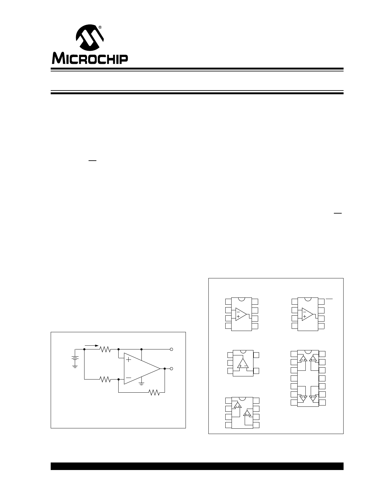
Package Types
V
DD
I
DD
MCP6031
100 k
Ω
1 M
Ω
1.4V
V
OUT
High Side Battery Current Sensor
10
Ω
to
5.5V
I
DD
V
DD
V
OUT
–
10 V/V
(
) 10
Ω
(
)
⋅
------------------------------------------
=
V
IN
+
V
IN
–
V
SS
V
DD
V
OUT
1
2
3
4
8
7
6
5 NC
NC
NC
V
INA
+
V
INA
–
V
SS
1
2
3
4
8
7
6
5
V
OUTA
V
DD
V
OUTB
V
INB
–
V
INB
+
MCP6031
DFN, SOIC, MSOP
MCP6032
SOIC, MSOP
V
IN
+
V
IN
–
V
SS
V
DD
V
OUT
1
2
3
4
8
7
6
5 NC
CS
NC
MCP6033
DFN, SOIC, MSOP
V
INA
+
V
INA
–
V
DD
1
2
3
4
14
13
12
11
V
OUTA
V
OUTD
V
IND
–
V
IND
+
V
SS
MCP6034
SOIC, TSSOP
V
INB
+ 5
10 V
INC
+
V
INB
– 6
9
V
OUTB
7
8 V
OUTC
V
INC
–
V
IN
+
V
SS
V
IN
–
1
2
3
5
4
V
DD
V
OUT
MCP6031
SOT-23-5
0.9 µA, High Precision Op Amps
MCP6031/2/3/4
DS22041B-page 2
© 2008 Microchip Technology Inc.
1.0
ELECTRICAL
CHARACTERISTICS
Absolute Maximum Ratings †
V
DD
– V
SS
........................................................................7.0V
Current at Input Pins .....................................................±2 mA
Analog Inputs (V
IN
+
, V
IN
-
)†† .......... V
SS
– 1.0V to V
DD
+ 1.0V
All Other Inputs and Outputs ......... V
SS
– 0.3V to V
DD
+ 0.3V
Difference Input Voltage ...................................... |V
DD
– V
SS
|
Output Short-Circuit Current .................................continuous
Current at Output and Supply Pins ............................±30 mA
Storage Temperature.....................................-65°C to +150°C
Maximum Junction Temperature (T
J
) .......................... +150°C
ESD protection on all pins (HBM; MM)
................ ≥ 4 kV; 400V
† Notice: Stresses above those listed under “Absolute
Maximum Ratings” may cause permanent damage to
the device. This is a stress rating only and functional
operation of the device at those or any other conditions
above those indicated in the operational listings of this
specification is not implied. Exposure to maximum rat-
ing conditions for extended periods may affect device
reliability.
†† See 4.1.2 “Input Voltage And Current Limits”
DC ELECTRICAL SPECIFICATIONS
Electrical Characteristics: Unless otherwise indicated, V
DD
= +1.8V to +5.5V, V
SS
=GND, T
A
= +25°C, V
CM
= V
DD
/2,
V
OUT
≈ V
DD
/2, V
L
= V
DD
/2, R
L
= 1 M
Ω to V
L
and CS is tied low. (Refer to
Figure 1-2
and
Figure 1-3
).
Parameters
Sym
Min
Typ
Max
Units
Conditions
Input Offset
Input Offset Voltage
V
OS
-150
—
+150
µV
V
DD
= 3.0V, V
CM
= V
DD
/3
Input Offset Drift with Temperature
ΔV
OS
/
ΔT
A
—
±3.0
—
µV/°C T
A
= -40°C to +125°C,
V
DD
= 3.0V, V
CM
= V
DD
/3
Power Supply Rejection Ratio
PSRR
70
88
—
dB
V
CM
= V
SS
Input Bias Current and Impedance
Input Bias Current
I
B
—
±1.0
100
pA
I
B
—
60
—
pA
T
A
= +85°C
I
B
—
2000
5000
pA
T
A
= +125°C
Input Offset Current
I
OS
—
±1.0
—
pA
Common Mode Input Impedance
Z
CM
—
10
13
||6
—
Ω||pF
Differential Input Impedance
Z
DIFF
—
10
13
||6
—
Ω||pF
Common Mode
Common Mode Input Voltage
Range
V
CMR
V
SS
− 0.3
—
V
DD
+ 0.3
V
Common Mode Rejection Ratio
CMRR
70
95
—
dB
V
CM
= -0.3V to 2.1V,
V
DD
= 1.8V
72
93
—
dB
V
CM
= -0.3V to 5.8V,
V
DD
= 5.5V
70
89
—
dB
V
CM
= 2.75V to 5.8V,
V
DD
= 5.5V
72
93
—
dB
V
CM
= -0.3V to 2.75V,
V
DD
= 5.5V
Open-Loop Gain
DC Open-Loop Gain
(Large Signal)
A
OL
95
115
—
dB
0.2V < V
OUT
< (V
DD
– 0.2V)
R
L
= 50 k
Ω to V
L
© 2008 Microchip Technology Inc.
DS22041B-page 3
MCP6031/2/3/4
AC ELECTRICAL SPECIFICATIONS
Output
Maximum Output Voltage Swing
V
OL
, V
OH
V
SS
+
10
—
V
DD
– 10
mV
R
L
= 50 k
Ω to V
L
,
0.5V input overdrive
Output Short-Circuit Current
I
SC
—
±5
—
mA
V
DD
= 1.8V
—
±23
—
mA
V
DD
= 5.5V
Power Supply
Supply Voltage
V
DD
1.8
—
5.5
V
Quiescent Current per Amplifier
I
Q
0.4
0.9
1.35
µA
I
O
= 0, V
CM
= V
DD,
V
DD
= 5.5V
Electrical Characteristics: Unless otherwise indicated, T
A
= +25°C, V
DD
= +1.8 to +5.5V, V
SS
= GND, V
CM
= V
DD
/2,
V
OUT
≈ V
DD
/2, V
L
= V
DD
/2, C
L
= 60 pF, R
L
= 1 M
Ω to V
L
and CS is tied low. (Refer to
Figure 1-2
and
Figure 1-3
).
Parameters
Sym
Min
Typ
Max
Units
Conditions
AC Response
Gain Bandwidth Product
GBWP
—
10
—
kHz
Phase Margin
PM
—
65
—
°
G = +1 V/V
Slew Rate
SR
—
4.0
—
V/ms
Noise
Input Noise Voltage
E
ni
—
3.9
—
µVp-p
f = 0.1 Hz to 10 Hz
Input Noise Voltage Density
e
ni
—
165
—
nV/
√Hz f = 1 kHz
Input Noise Current Density
i
ni
—
0.6
—
fA/
√Hz f = 1 kHz
DC ELECTRICAL SPECIFICATIONS (CONTINUED)
Electrical Characteristics: Unless otherwise indicated, V
DD
= +1.8V to +5.5V, V
SS
=GND, T
A
= +25°C, V
CM
= V
DD
/2,
V
OUT
≈ V
DD
/2, V
L
= V
DD
/2, R
L
= 1 M
Ω to V
L
and CS is tied low. (Refer to
Figure 1-2
and
Figure 1-3
).
Parameters
Sym
Min
Typ
Max
Units
Conditions
MCP6031/2/3/4
DS22041B-page 4
© 2008 Microchip Technology Inc.
MCP6033 CHIP SELECT ELECTRICAL CHARACTERISTICS
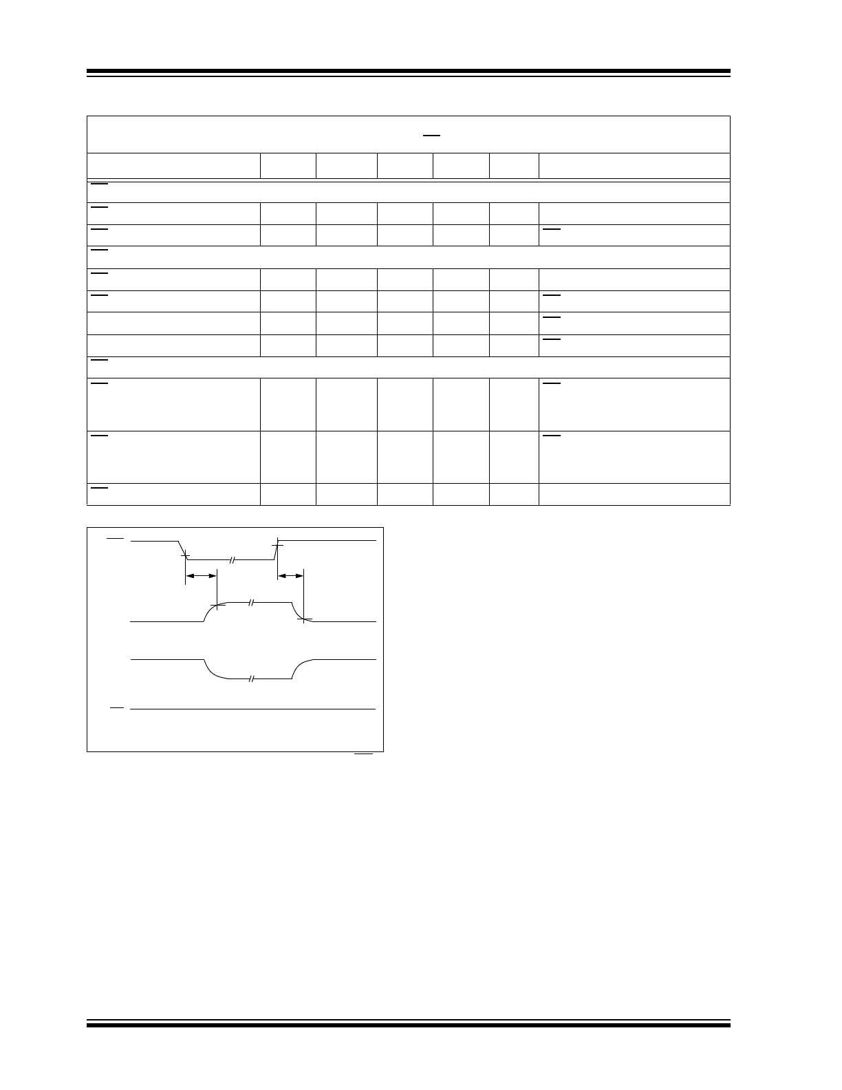
FIGURE 1-1:
Timing Diagram for the CS
Pin on the MCP6033.
Electrical Specifications: Unless otherwise indicated, V
DD
= +1.8V to +5.5V, V
SS
=GND, T
A
= +25°C, V
CM
= V
DD
/2,
V
OUT
= V
DD
/2, V
L
= V
DD
/2, C
L
= 60 pF, R
L
= 1 M
Ω to V
L
and CS is tied low (Refer to
Figure 1-1
).
Parameters
Sym
Min
Typ
Max
Units
Conditions
CS Low Specifications
CS Logic Threshold, Low
V
IL
V
SS
—
0.2V
DD
V
CS Input Current, Low
I
CSL
—
-10
—
pA
CS = V
SS
CS High Specifications
CS Logic Threshold, High
V
IH
0.8V
DD
V
DD
V
CS Input Current, High
I
CSH
—
10
—
pA
CS = V
DD
GND Current
I
SS
—
-400
—
pA
CS = V
DD
Amplifier Output Leakage
I
O(LEAK)
—
10
—
pA
CS = V
DD
CS Dynamic Specifications
CS Low to Amplifier Output
Turn-on Time
t
ON
—
4
100
ms
CS
≤ 0.2V
DD
to V
OUT
= 0.9V
DD
/2,
G = +1 V/V, V
IN
= V
DD
/2,
R
L
= 50 k
Ω to V
L
= V
SS.
CS High to Amplifier Output
High-Z
t
OFF
—
10
—
µs
CS
≥ 0.8V
DD
to V
OUT
= 0.1V
DD
/2,
G = +1 V/V, V
IN
= V
DD
/2,
R
L
= 50 k
Ω to V
L
= V
SS.
CS Hysteresis
V
HYST
—
0.3V
DD
—
V
V
IL
High-Z
t
ON
V
IH
CS
t
OFF
V
OUT
-400 pA
High-Z
I
SS
I
CS
10 pA
-400 pA
-0.9 µA
(typical)
(typical)
(typical)
(typical)
© 2008 Microchip Technology Inc.
DS22041B-page 5
MCP6031/2/3/4
TEMPERATURE SPECIFICATIONS
1.1
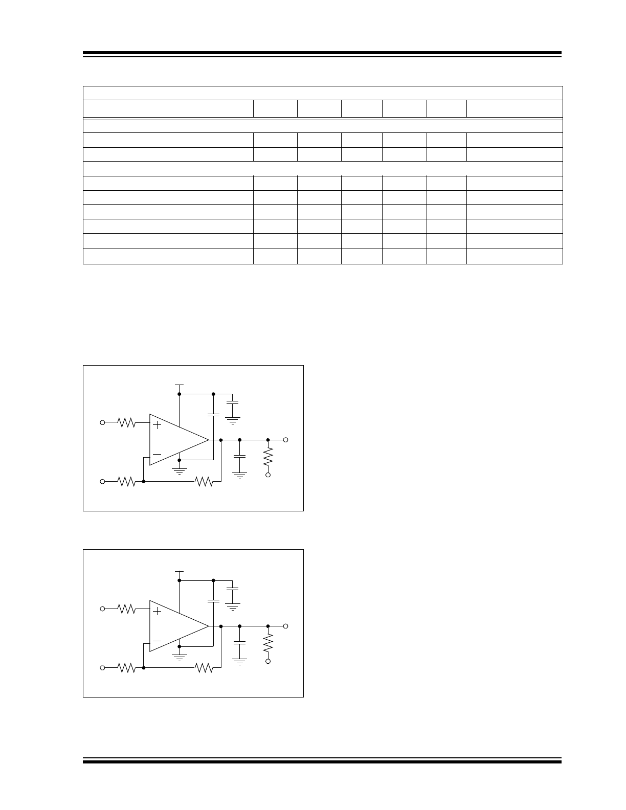
Test Circuits
The test circuits used for the DC and AC tests are
shown in
Figure 1-2
and
Figure 1-3
. The bypass
capacitors are laid out according to the rules discussed
in
Section 4.6 “Supply Bypass”.
FIGURE 1-2:
AC and DC Test Circuit for
Most Non-Inverting Gain Conditions.
FIGURE 1-3:
AC and DC Test Circuit for
Most Inverting Gain Conditions.
Electrical Characteristics: Unless otherwise indicated, V
DD
= +1.8V to +5.5V and V
SS
= GND.
Parameters
Sym
Min
Typ
Max
Units
Conditions
Temperature Ranges
Operating Temperature Range
T
A
-40
—
+125
°C
Note
Storage Temperature Range
T
A
-65
—
+150
°C
Thermal Package Resistances
Thermal Resistance, 5L-SOT-23
θ
JA
—
256
—
°C/W
Thermal Resistance, 8L-DFN (2x3)
θ
JA
—
84
—
°C/W
Thermal Resistance, 8L-SOIC
θ
JA
—
163
—
°C/W
Thermal Resistance, 8L-MSOP
θ
JA
—
206
—
°C/W
Thermal Resistance, 14L-SOIC
θ
JA
—
120
—
°C/W
Thermal Resistance, 14L-TSSOP
θ
JA
—
100
—
°C/W
Note:
The internal junction temperature (T
J
) must not exceed the absolute maximum specification of +150°C.
V
DD
MCP603X
R
G
R
F
R
N
V
OUT
V
IN
V
DD
/2
2.2 µF
C
L
R
L
V
L
0.1 µF
V
DD
MCP603X
R
G
R
F
R
N
V
OUT
V
IN
V
DD
/2
2.2 µF
C
L
R
L
V
L
0.1 µF
MCP6031/2/3/4
DS22041B-page 6
© 2008 Microchip Technology Inc.
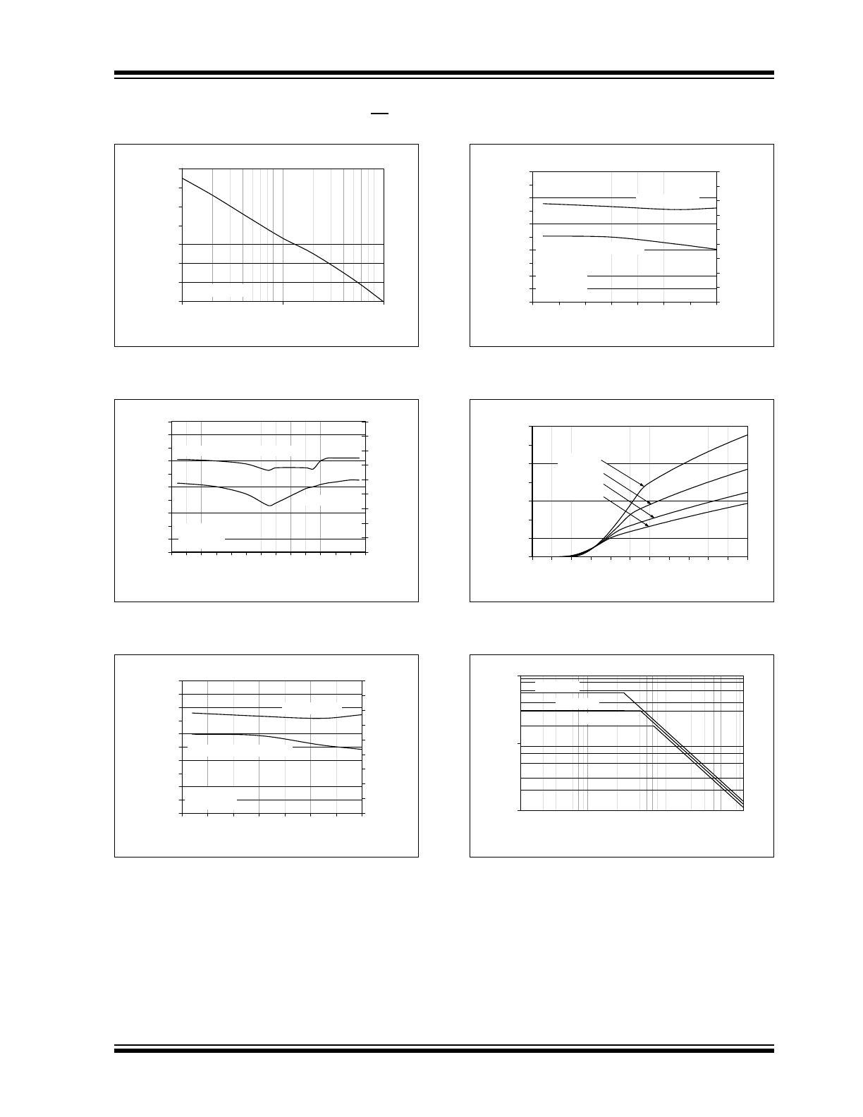
2.0
TYPICAL PERFORMANCE CURVES
Note: Unless otherwise indicated, T
A
= +25°C, V
DD
= +1.8V to +5.5V, V
SS
= GND, V
CM
= V
DD
/2, V
OUT
≈ V
DD
/2,
V
L
= V
DD
/2, R
L
= 1 M
Ω to V
L
, C
L
= 60 pF and CS is tied low.
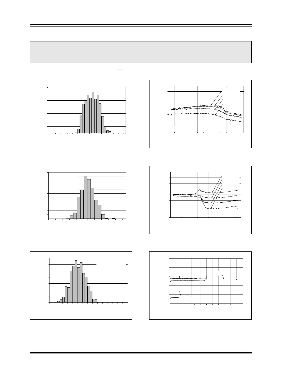
FIGURE 2-1:
Input Offset Voltage with
V
DD
= 3.0V.
FIGURE 2-2:
Input Offset Voltage Drift
with V
DD
= 3.0V and T
A
≤
+85°C.
FIGURE 2-3:
Input Offset Voltage Drift
with V
DD
= 3.0V and T
A
≥
+85°C.
FIGURE 2-4:
Input Offset Voltage vs.
Common Mode Input Voltage with V
DD
= 5.5V.
FIGURE 2-5:
Input Offset Voltage vs.
Common Mode Input Voltage with V
DD
= 1.8V.
FIGURE 2-6:
Input Offset Voltage vs.
Output Voltage.
Note:
The graphs and tables provided following this note are a statistical summary based on a limited number of
samples and are provided for informational purposes only. The performance characteristics listed herein
are not tested or guaranteed. In some graphs or tables, the data presented may be outside the specified
operating range (e.g., outside specified power supply range) and therefore outside the warranted range.
0%
2%
4%
6%
8%
10%
12%
14%
-150 -120 -90 -60 -30
0
30 60 90 120 150
Input Offset Voltage (μV)
Percentage of
Occurences
640 Samples
V
DD
= 3.0V
V
CM
= V
DD
/3
0%
2%
4%
6%
8%
10%
12%
14%
16%
18%
20%
22%
-20 -16 -12 -8
-4
0
4
8
12 16 20
Input Offset Drift with Temperature (μV/°C)
Percentag
e of
O
ccu
rences
640 Samples
V
DD
= 3.0V
V
CM
= V
DD
/3
T
A
= -40°C to +85°C
0%
2%
4%
6%
8%
10%
12%
14%
-30 -24 -18 -12 -6
0
6
12
18
24
30
Input Offset Drift with Temperature (μV/°C)
Percent
age of Occurences
640 Samples
V
DD
= 3.0V
V
CM
= V
DD
/3
T
A
= +85°C to +125°C
-400
-300
-200
-100
0
100
200
300
400
-0
.5
0.
0
0.
5
1.
0
1.
5
2.
0
2.
5
3.
0
3.
5
4.
0
4.
5
5.
0
5.
5
6.
0
Common Mode Input Voltage (V)
Input Of
fset
V
o
lt
age (
μ
V)
T
A
= -40°C
T
A
= +25°C
T
A
= +85°C
T
A
= +125°C
V
DD
= 5.5V
-400
-300
-200
-100
0
100
200
300
400
-0
.4
-0
.2
0.
0
0.
2
0.
4
0.
6
0.
8
1.
0
1.
2
1.
4
1.
6
1.
8
2.
0
2.
2
Common Mode Input Voltage (V)
In
pu
t
O
ff
set
Vol
tag
e (
μ
V)
T
A
= -40°C
T
A
= +25°C
T
A
= +85°C
T
A
= +125°C
V
DD
= 1.8V
-250
-200
-150
-100
-50
0
50
100
150
200
250
0.0 0.5 1.0 1.5 2.0 2.5 3.0 3.5 4.0 4.5 5.0 5.5 6.0
Output Voltage (V)
Input O
ffse
t Vo
lt
ag
e
(μ
V)
V
DD
= 1.8V
V
DD
= 5.5V
V
DD
= 3.0V
© 2008 Microchip Technology Inc.
DS22041B-page 7
MCP6031/2/3/4
Note: Unless otherwise indicated, T
A
= +25°C, V
DD
= +1.8V to +5.5V, V
SS
= GND, V
CM
= V
DD
/2, V
OUT
≈ V
DD
/2,
V
L
= V
DD
/2, R
L
= 1 M
Ω to V
L
, C
L
= 60 pF and CS is tied low.
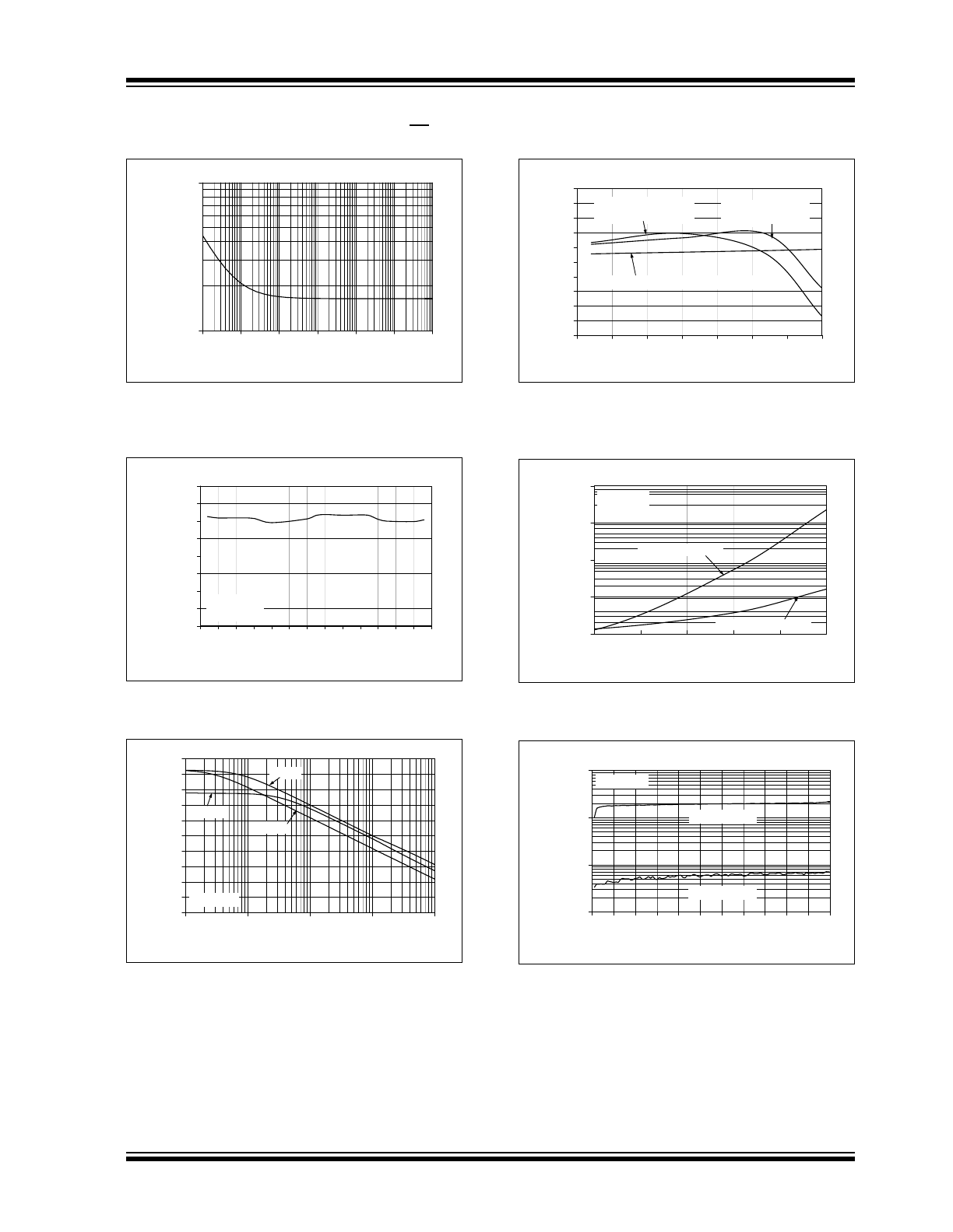
FIGURE 2-7:
Input Noise Voltage Density
vs. Frequency.
FIGURE 2-8:
Input Noise Voltage Density
vs. Common Mode Input Voltage.
FIGURE 2-9:
Common Mode Rejection
Ratio, Power Supply Rejection Ratio vs.
Frequency.
FIGURE 2-10:
Common Mode Rejection
Ratio, Power Supply Rejection Ratio vs. Ambient
Temperature.
FIGURE 2-11:
Input Bias, Offset Currents
vs. Ambient Temperature.
FIGURE 2-12:
Input Bias Current vs.
Common Mode Input Voltage.
100
1,000
1E-1
1E+0
1E+1
1E+2
1E+3
1E+4
1E+5
Frequency (Hz)
In
put Nois
e Vol
ta
g
e
D
ensity
(nV
/√
Hz
)
0.1
1
10
100
1k
10k
100k
0
25
50
75
100
125
150
175
200
-0
.5
0.
0
0.
5
1.
0
1.
5
2.
0
2.
5
3.
0
3.
5
4.
0
4.
5
5.
0
5.
5
6.
0
Common Mode Input Voltage (V)
In
pu
t No
is
e V
o
lt
ag
e D
ens
it
y
(nV/
√Hz
)
f = 1 kHz
V
DD
= 5.5V
0
10
20
30
40
50
60
70
80
90
100
0.1
1
10
100
1000
Frequency (Hz)
CMR
R
, P
S
R
R
(dB)
PSRR-
PSRR+
CMRR
V
DD
= 5.5V
60
65
70
75
80
85
90
95
100
105
110
-50
-25
0
25
50
75
100
125
Ambient Temperature (°C)
PSR
R,
C
M
RR
(
d
B)
PSRR (V
DD
= 1.8V to 5.5V, V
CM
= V
SS
)
CMRR (V
DD
= 1.8V,
V
CM
= -0.3V to 2.1V)
CMRR (V
DD
= 5.5V,
V
CM
= -0.3V to 5.8V)
1
10
100
1000
10000
25
45
65
85
105
125
Ambient Temperature (°C)
Input
B
ia
s
a
nd O
ff
s
et
C
u
rre
n
ts
(pA
)
V
DD
= 5.5V
V
CM
= V
DD
Input Bias Current
Input Offset Current
10
100
1000
10000
0.0 0.5 1.0 1.5 2.0 2.5 3.0 3.5 4.0 4.5 5.0 5.5
Common Mode Input Voltage (V)
Inpu
t B
ia
s C
u
rren
t (p
A)
T
A
= +125°C
T
A
= +85°C
V
DD
= 5.5V
MCP6031/2/3/4
DS22041B-page 8
© 2008 Microchip Technology Inc.
Note: Unless otherwise indicated, T
A
= +25°C, V
DD
= +1.8V to +5.5V, V
SS
= GND, V
CM
= V
DD
/2, V
OUT
≈ V
DD
/2,
V
L
= V
DD
/2, R
L
= 1 M
Ω to V
L
, C
L
= 60 pF and CS is tied low.
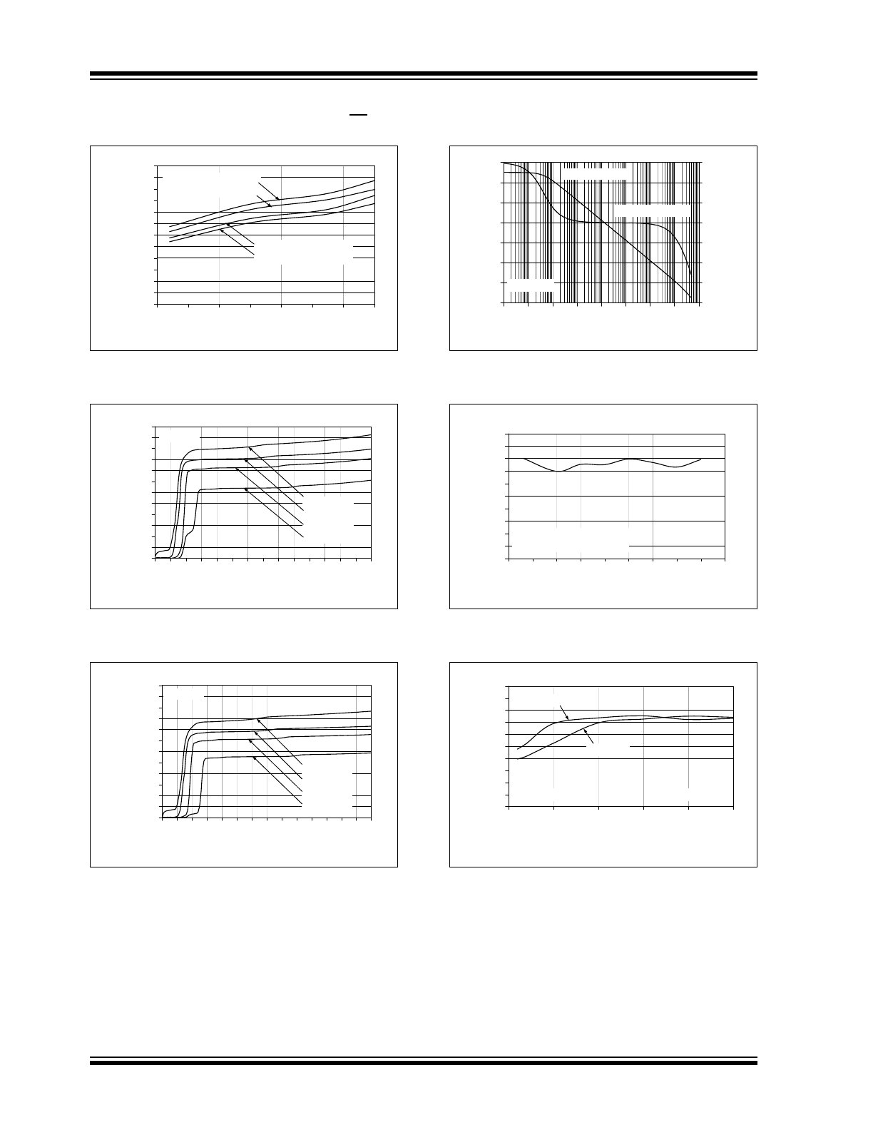
FIGURE 2-13:
Quiescent Current vs
Ambient Temperature.
FIGURE 2-14:
Quiescent Current vs.
Power Supply Voltage with V
CM
= V
DD
.
FIGURE 2-15:
Quiescent Current vs.
Power Supply Voltage with V
CM
= V
SS
.
FIGURE 2-16:
Open-Loop Gain, Phase vs.
Frequency.
FIGURE 2-17:
DC Open-Loop Gain vs.
Power Supply Voltage.
FIGURE 2-18:
DC Open-Loop Gain vs.
Output Voltage Headroom.
0.0
0.1
0.2
0.3
0.4
0.5
0.6
0.7
0.8
0.9
1.0
1.1
1.2
-50
-25
0
25
50
75
100
125
Ambient Temperature (°C)
Quies
c
en
t Curre
nt
(μ
A/Amplifier)
V
DD
= 5.5V @ V
CM
= V
DD
V
DD
= 1.8V @ V
CM
= V
DD
V
DD
= 5.5V @ V
CM
= V
SS
V
DD
= 1.8V @ V
CM
= V
SS
0.0
0.1
0.2
0.3
0.4
0.5
0.6
0.7
0.8
0.9
1.0
1.1
1.2
0.
0
0.
5
1.
0
1.
5
2.
0
2.
5
3.
0
3.
5
4.
0
4.
5
5.
0
5.
5
6.
0
6.
5
7.
0
Power Supply Voltage (V)
Qu
iesc
en
t C
u
rr
en
t
(μ
A/Amplif
ie
r)
V
CM
= V
DD
T
A
= +125°C
T
A
= +85°C
T
A
= +25°C
T
A
= -40°C
0.0
0.1
0.2
0.3
0.4
0.5
0.6
0.7
0.8
0.9
1.0
1.1
1.2
0.
0
0.
5
1.
0
1.
5
2.
0
2.
5
3.
0
3.
5
4.
0
4.
5
5.
0
5.
5
6.
0
6.
5
7.
0
Power Supply Voltage (V)
Quie
sce
n
t Curre
n
t
(μ
A/
Am
pl
if
ie
r)
V
CM
= V
SS
T
A
= +125°C
T
A
= +85°C
T
A
= +25°C
T
A
= -40°C
-20
0
20
40
60
80
100
120
0
0.01 0.1
1
10 100 100
0
100
00
1E+
05
Frequency (Hz)
Open-Loop Gain (V/V
)
-210
-180
-150
-120
-90
-60
-30
0
Open-
Loop P
h
ase (
°)
Open-Loop Gain
Open-Loop Phase
V
DD
= 5.5V
0.001 0.01
1k 10k 100k
80
85
90
95
100
105
110
115
120
125
130
1.5 2.0 2.5 3.0 3.5 4.0 4.5 5.0 5.5 6.0
Power Supply Voltage V
DD
(V)
DC
Ope
n
-L
oop
G
ain (
d
B)
R
L
= 50 kΩ
V
SS
+ 0.2V < V
OUT
< V
DD
- 0.2V
80
85
90
95
100
105
110
115
120
125
130
0.00
0.05
0.10
0.15
0.20
0.25
Output Voltage Headroom
V
DD
- V
OUT
or V
OUT
- V
SS
(V)
DC
O
p
en
-L
o
o
p
Ga
in
(d
B)
R
L
= 50 kΩ
V
DD
= 5.5V
V
DD
= 1.8V
Large Signal A
OL
© 2008 Microchip Technology Inc.
DS22041B-page 9
MCP6031/2/3/4
Note: Unless otherwise indicated, T
A
= +25°C, V
DD
= +1.8V to +5.5V, V
SS
= GND, V
CM
= V
DD
/2, V
OUT
≈ V
DD
/2,
V
L
= V
DD
/2, R
L
= 1 M
Ω to V
L
, C
L
= 60 pF and CS is tied low.
FIGURE 2-19:
Channel-to-Channel
Separation vs. Frequency ( MCP6032/4 only).
FIGURE 2-20:
Gain Bandwidth Product,
Phase Margin vs. Common Mode Input Voltage.
FIGURE 2-21:
Gain Bandwidth Product,
Phase Margin vs. Ambient Temperature.
FIGURE 2-22:
Gain Bandwidth Product,
Phase Margin vs. Ambient Temperature.
FIGURE 2-23:
Ouput Short Circuit Current
vs. Power Supply Voltage.
FIGURE 2-24:
Output Voltage Swing vs.
Frequency.
60
70
80
90
100
110
120
130
100
1,000
10,000
Frequency (Hz)
C
h
anne
l-
to
-Ch
a
nn
el
Se
pe
ra
ti
on
(
d
B
)
Input Referred
0
2
4
6
8
10
12
14
16
18
20
-0
.5
0.
0
0.
5
1.
0
1.
5
2.
0
2.
5
3.
0
3.
5
4.
0
4.
5
5.
0
5.
5
6.
0
Common Mode Input Voltage (V)
Gain Bandwidt
h
P
roduct
(k
H
z)
0
20
40
60
80
100
120
140
160
180
P
h
as
e M
ar
g
in
(
°)
Gain Bandwidth Product
Phase Margin
V
DD
= 5.5V
G = +1 V/V
0
2
4
6
8
10
12
14
16
18
20
-50
-25
0
25
50
75
100 125
Ambient Temperature (°C)
G
ain B
andwi
d
th
Prod
uc
t
(k
Hz)
0
10
20
30
40
50
60
70
80
90
Ph
as
e Ma
rg
in
(
°)
Gain Bandwidth Product
Phase Margin
V
DD
= 5.5V
G = +1 V/V
0
2
4
6
8
10
12
14
16
18
20
-50
-25
0
25
50
75
100 125
Ambient Temperature (°C)
Gain Ba
ndwi
d
th
Prod
uct
(k
Hz)
0
10
20
30
40
50
60
70
80
90
P
h
as
e Ma
rgin
(°
)
Gain Bandwidth Product
Phase Margin
V
DD
= 1.8V
G = +1 V/V
0
5
10
15
20
25
30
35
0.0 0.5 1.0 1.5 2.0 2.5 3.0 3.5 4.0 4.5 5.0 5.5
Power Supply Voltage (V)
Ou
tput S
hort Ci
rcu
it Cu
rre
n
t
(mA
)
T
A
= -40°C
T
A
= +25°C
T
A
= +85°C
T
A
= +125°C
0.1
1
10
10
100
1000
10000
Frequency (Hz)
Out
p
ut
Vol
tage S
wing (
V
P-
P
)
V
DD
= 1.8V
V
DD
= 3.0V
V
DD
= 5.5V
1K
10K
MCP6031/2/3/4
DS22041B-page 10
© 2008 Microchip Technology Inc.
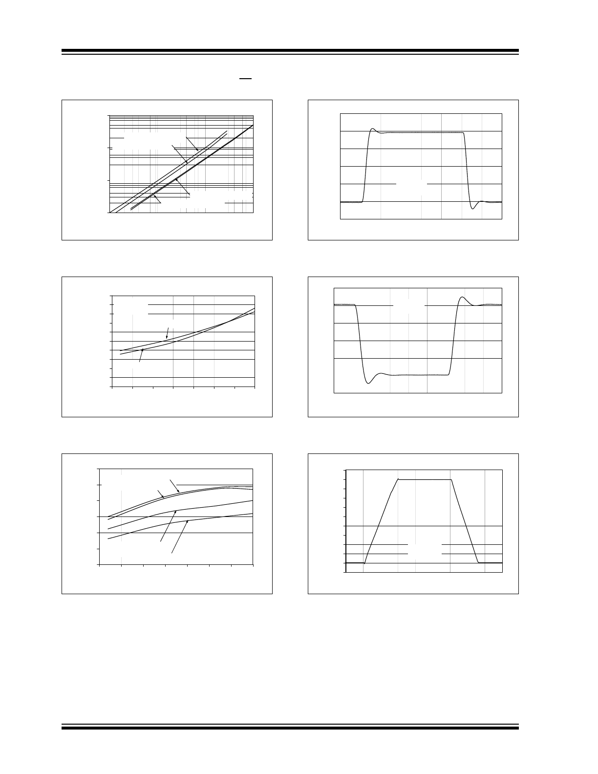
Note: Unless otherwise indicated, T
A
= +25°C, V
DD
= +1.8V to +5.5V, V
SS
= GND, V
CM
= V
DD
/2, V
OUT
≈ V
DD
/2,
V
L
= V
DD
/2, R
L
= 1 M
Ω to V
L
, C
L
= 60 pF and CS is tied low.
FIGURE 2-25:
Output Voltage Headroom
vs. Output Current.
FIGURE 2-26:
Output Voltage Headroom
vs. Ambient Temperature.
FIGURE 2-27:
Slew Rate vs. Ambient
Temperature.
FIGURE 2-28:
Small Signal Non-Inverting
Pulse Response.
FIGURE 2-29:
Small Signal Inverting Pulse
Response.
FIGURE 2-30:
Large Signal Non-Inverting
Pulse Response.
1
10
100
1000
Output Current (A)
Output
Voltag
e
He
ad
room
V
DD
-
V
OH
, V
OL
-
V
SS
(m
V)
V
DD
- V
OH
@ V
DD
= 1.8V
V
OL
- V
SS
@ V
DD
= 1.8V
V
DD
- V
OH
@ V
DD
= 5.5V
V
OL
- V
SS
@ V
DD
= 5.5V
10μ
1m
10m
100µ
0.0
0.5
1.0
1.5
2.0
2.5
3.0
3.5
4.0
4.5
5.0
-50
-25
0
25
50
75
100
125
Ambient Temperature (°C)
Ou
tp
ut
Vol
tag
e He
ad
ro
om
V
DD
-
V
OH
or
V
SS
-
V
OL
(m
V)
V
DD
= 5.5V
R
L
= 50 kΩ
V
SS
- V
OL
V
DD
- V
OH
1.0
2.0
3.0
4.0
5.0
6.0
7.0
-50
-25
0
25
50
75
100
125
Ambient Temperature (°C)
S
lew
R
a
te
(V
/m
s)
Falling Edge, V
DD
= 5.5V
Falling Edge, V
DD
= 1.8V
Rising Edge, V
DD
= 5.5V
Rising Edge, V
DD
= 1.8V
Time (100 μs/Div)
O
u
tp
u
t V
o
lt
ag
e
(20
mV/
d
iv
)
V
DD
= 5.5V
G = +1 V/V
Ou
tp
u
t Vo
lt
ag
e (
20 mV/
d
iv
)
V
DD
= 5.5V
G = -1 V/V
Time (100 μs/Div)
0.0
0.5
1.0
1.5
2.0
2.5
3.0
3.5
4.0
4.5
5.0
5.5
Time (0.5 ms/div)
Ou
tput V
o
lt
ag
e (V
)
V
DD
= 5.5V
G = +1 V/V