
2017 Microchip Technology Inc.
DS20005741A-page 1
PL611S-18-XXX
Features
• Designed for Very Low Power Applications
• Accepts Crystal or Reference Clock Inputs
• Input Frequency:
- Fundamental Crystal: 10 MHz to 50 MHz
- Reference Input: 1 MHz to 125 MHz
• Accepts >0.1V Reference Signal Input Voltage
• Output Frequency 0.5 kHz to 125 MHz CMOS
- 65 MHz at 1.8V Operation
- 90 MHz at 2.5V Operation
- 125 MHz at 3.3V Operation
• One Programmable I/O Pin Can be Configured as
OE, PDB, FSEL, or CLK1
• Low Current Consumption
- <1.0 mA with 27 MHz and 32 kHz Outputs
- <5 µA when PDB is Activated
• Single 1.8V ~ 3.3V, ±10% Power Supply
• Operating Temperature Range:
- –40°C to +85°C (Industrial)
- 0°C to +70°C (Commercial)
• Available in 6-pin TDFN or SOT-23
GREEN/RoHS-Compliant Packaging
General Description
The PL611s-18-xxx is a general purpose frequency
synthesizer and a member of the PicoPLL family, the
world’s smallest programmable clocks. PL611s-18-xxx
offers the versatility of using a single crystal (MHz) or
reference clock input and producing up to two
(kHz/MHz) system clocks, or a combination of
reference and low frequency outputs. The
PL611s-18-xxx is designed for low-power applications
with very stringent space requirements and consumes,
for example, ~1.0 mA while producing two distinct
outputs of 27 MHz and 32 kHz. The power down
feature of the PL611s-18-xxx, when activated, allows
the IC to consume less than 5 µA of power.
The PL611s-18-xxx fits in a small DFN-6L or SOT23-6L
package. Cascading of the PL611s-18-xxx with other
programmable clocks allows the generation of system
level clocking requirements, thereby reducing the
overall system implementation cost.
In addition, one programmable I/O pin can be
configured as Output Enable (OE), Frequency
switching (FSEL), Power Down (PDB) input, or CLK1
(CLK0, FREF, FREF/2) output.
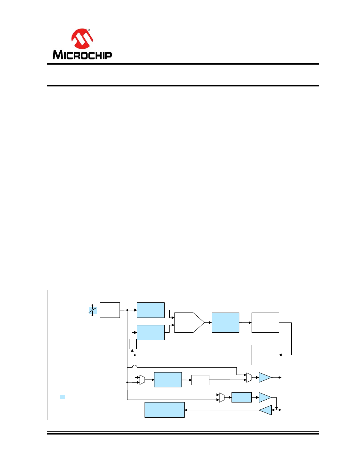
Block Diagram
PL611
S
-18-
XXX
Phase
Detector
Charge
Pump
Loop
Filter
VCO
XIN/FIN
XOUT
R-Counter
(5-bit)
F
VCO
= F
REF
* (2 * M/R)
F
OUT
= F
VCO
/ (2 * P)
CLK0
F
REF
OE, PDB,
FSEL, CLK1
XTAL
OSC
M-Counter
(8-bit)
Programmable
CLoad
Programmable Function
P-Counter
(14-bit)
÷2
÷1, ÷2
Programming
Logic
÷2
0.5 kHz to 125 MHz, MHz-to-kHz Programmable Clock

PL611S-18-XXX
DS20005741A-page 2
2017 Microchip Technology Inc.
1.0
ELECTRICAL CHARACTERISTICS
Absolute Maximum Ratings †
Supply Voltage (V
DD
) ................................................................................................................................ –0.5V to +4.6V
Input Voltage (V
IN
).............................................................................................................................–0.5V to V
DD
+ 0.5V
Output Voltage (V
OUT
).......................................................................................................................–0.5V to V
DD
+ 0.5V
ESD Rating (
Note 1
)...................................................................................................................................................2 kV
Operating Ratings ‡
Supply Voltage (V
IN
).............................................................................................................................. +1.62V to +3.63V
†
Notice: Stresses above those listed under “Absolute Maximum Ratings” may cause permanent damage to the device.
This is a stress rating only and functional operation of the device at those or any other conditions above those indicated
in the operational sections of this specification is not intended. Exposure to maximum rating conditions for extended
periods may affect device reliability. Parts are tested to commercial grade only.
‡
Notice: The device is not guaranteed to function outside its operating ratings.
Note 1:
Devices are ESD sensitive. Handling precautions are recommended. Human body model, 1.5 kΩ in series
with 100 pF.
2017 Microchip Technology Inc.
DS20005741A-page 3
PL611S-18-XXX
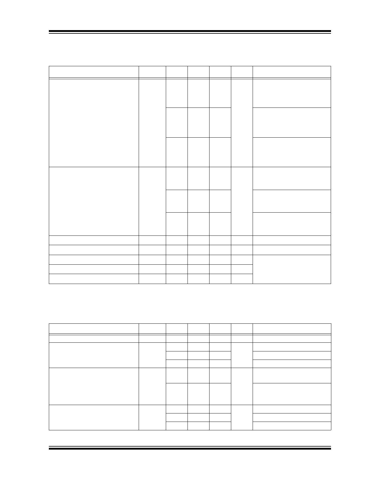
TABLE 1-1:
DC ELECTRICAL CHARACTERISTICS (
Note 1
)
Electrical Characteristics:
V
IN
= 3.3V; C
L
= 15 pF; T
A
= +25°C, bold values indicate –40°C ≤ T
A
≤ +85°C, unless
noted.
Parameters
Sym.
Min.
Typ.
Max.
Units
Conditions
Supply Current, Power Down State
I
DD
—
3.95
10.0
mA
V
DD
= 3.3V, 27 MHz Xtal input,
F
VCO
= 81 MHz, CLK0 =
32.768 kHz, CLK1 = 27 MHz,
Load = 15 pF
—
2.35
3.5
V
DD
= 2.5V, 27 MHz Xtal input,
F
VCO
= 81 MHz, CLK0 =
32.768 kHz, CLK1 = 27 MHz,
Load = 10 pF
—
1.30
2.0
V
DD
= 1.8V, 27 MHz Xtal input,
F
VCO
= 81 MHz, CLK0 =
32.768 kHz, CLK1 = 27 MHz,
Load = 5 pF
PLL Off Supply Current, Dynamic
I
DD
—
2.75
9.0
mA
V
DD
= 3.3V, 27 MHz Xtal input,
CLK0 = 32.768 kHz, CLK1 =
27 MHz, Load = 15 pF
—
1.30
2.0
V
DD
= 2.5V, 27 MHz Xtal input,
CLK0 = 32.768 kHz, CLK1 =
27 MHz, Load = 10 pF
—
0.9
1.4
V
DD
= 1.8V, 27 MHz Xtal input,
CLK0 = 32.768 kHz, CLK1 =
27 MHz, Load = 5 pF
Supply Current, Power Down State
I
DD
—
—
5
µA
When PDB = 0
Operating Voltage
V
DD
1.62
—
3.63
V
—
Output Current, Low Drive
I
OLD
4
—
—
mA
V
OL
= 0.4V, V
OH
= V
DD
– 0.9V,
V
DD
= 3.3V
Output Current, Standard Drive
I
OSD
8
—
—
mA
Output Current, High Drive
I
OHD
16
—
—
mA
Note 1:
Specification for packaged product only.
TABLE 1-2:
AC ELECTRICAL CHARACTERISTICS (
Note 1
)
Electrical Characteristics:
V
IN
= 3.3V; C
L
= 15 pF; T
A
= +25°C, bold values indicate –40°C ≤ T
A
≤ +85°C, unless
noted.
Parameters
Sym.
Min.
Typ.
Max.
Units
Conditions
Crystal Input Frequency
f
IN(XTAL)
10
—
50
MHz
Fundamental Crystal
Input Frequency
f
IN
1
—
125
MHz
V
DD
= 3.3V
1
—
90
V
DD
= 2.5V
1
—
65
V
DD
= 1.8V
Input (f
IN
) Signal Amplitude
—
0.8
—
V
DD
V
PP
Internally AC-Coupled (high
frequency)
0.1
—
V
DD
Internally AC-Coupled (low
frequency) 3.3V ≤50 MHz,
2.5V ≤40 MHz, 1.8V ≤15 MHz
Output Frequency
f
OUT
—
—
125
MHz
V
DD
= 3.3V
—
—
90
V
DD
= 2.5V
—
—
65
V
DD
= 1.8V
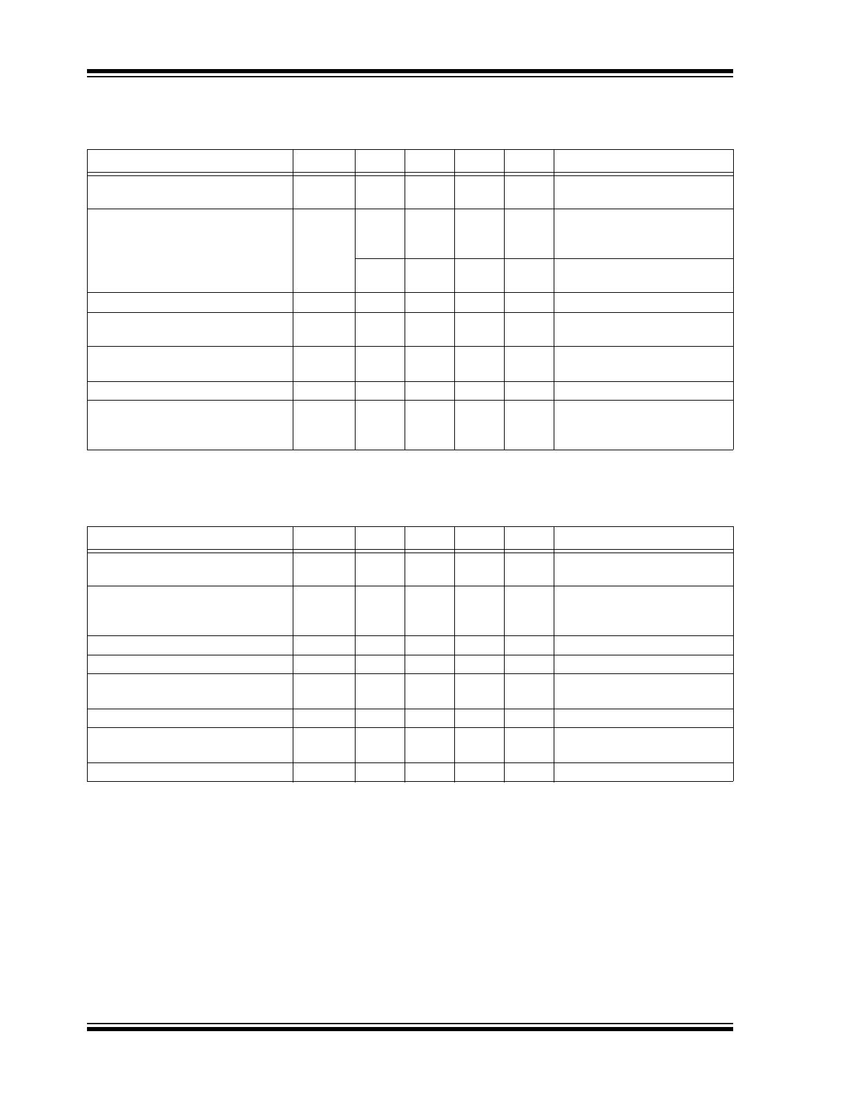
PL611S-18-XXX
DS20005741A-page 4
2017 Microchip Technology Inc.
Settling Time
—
—
—
2
ms
At power-up (after V
DD
increases over 1.62V)
Output Enable Time
t
OE
—
—
100
µs
OE function; T
A
= +25°C,
15 pF load. Add one clock
period for a usable output.
—
—
2
ms
PDB function; T
A
= +25°C,
15 pF load.
V
DD
Sensitivity
—
–2
—
2
ppm
Frequency vs. V
DD
±10%
Output Rise Time
t
r
—
2
3
ns
15 pF load, 10/90% V
DD
,
Standard Drive, 3.3V
Output Fall Time
t
f
—
2
3
ns
15 pF load, 90/10% V
DD
,
Standard Drive, 3.3V
Duty Cycle
—
45
50
55
%
V
DD
/2
Period Jitter, Peak-to-Peak (
Note 2
)
—
—
70
—
ps
With capacitive decoupling
between V
DD
and GND.
10,000 samples measured.
Note 1:
Specification for packaged product only.
2:
Jitter performance depends on the programming parameters.
TABLE 1-2:
AC ELECTRICAL CHARACTERISTICS (
Note 1
) (CONTINUED)
Electrical Characteristics:
V
IN
= 3.3V; C
L
= 15 pF; T
A
= +25°C, bold values indicate –40°C ≤ T
A
≤ +85°C, unless
noted.
Parameters
Sym.
Min.
Typ.
Max.
Units
Conditions
TABLE 1-3:
CRYSTAL SPECIFICATIONS
Parameters
Sym.
Min.
Typ.
Max.
Units
Conditions
Fundamental Crystal Resonator
Frequency
F
XIN
10
—
50
MHz
—
Crystal Loading Rating
(The IC can be programmed for any
value in this range.)
C
L(XTAL)
8
—
12
pF
—
Maximum Sustainable Drive Level
—
—
—
100
µW
—
Operating Drive Level
—
—
30
—
µW
—
Metal Can Crystal Shunt
Capacitance
C0
—
—
5.5
pF
—
Metal Can Crystal ESR max.
ESR
—
—
50
Ω
—
Small SMD Crystal Shunt
Capacitance
C0
—
—
2.5
pF
—
Small SMD Crystal ESR max.
ESR
—
—
80
Ω
—
2017 Microchip Technology Inc.
DS20005741A-page 5
PL611S-18-XXX
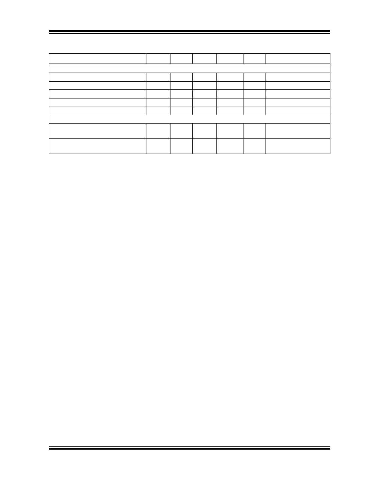
TEMPERATURE SPECIFICATIONS (
Note 1
)
Parameters
Sym.
Min.
Typ.
Max.
Units
Conditions
Temperature Ranges
Storage Temperature Range
T
S
–65
—
+150
°C
—
Ambient Operating Temperature
T
A
–40
—
+85
°C
Industrial
Ambient Operating Temperature
T
A
0
—
+70
°C
Commercial
Junction Operating Temperature
T
J
—
—
+110
°C
—
Lead Temperature
—
—
—
+260
°C
Soldering, 10 sec.
Thermal Resistance
Junction Thermal Resistance, 6-Ld
TDFN
θ
JA
—
100
—
°C/W
—
Junction Thermal Resistance, 6-Ld
SOT-23
θ
JA
—
192
—
°C/W
—
Note 1:
Exposure of the device under conditions beyond the limits specified by the maximum ratings for extended
periods may cause permanent damage to the device and affect product reliability. These conditions
represent a stress rating only, and functional operations of the device at these or any other conditions
above the operational limits noted in this specification is not implied. Operating temperature is guaranteed
by design. Parts are tested to commercial grade only.
PL611S-18-XXX
DS20005741A-page 6
2017 Microchip Technology Inc.
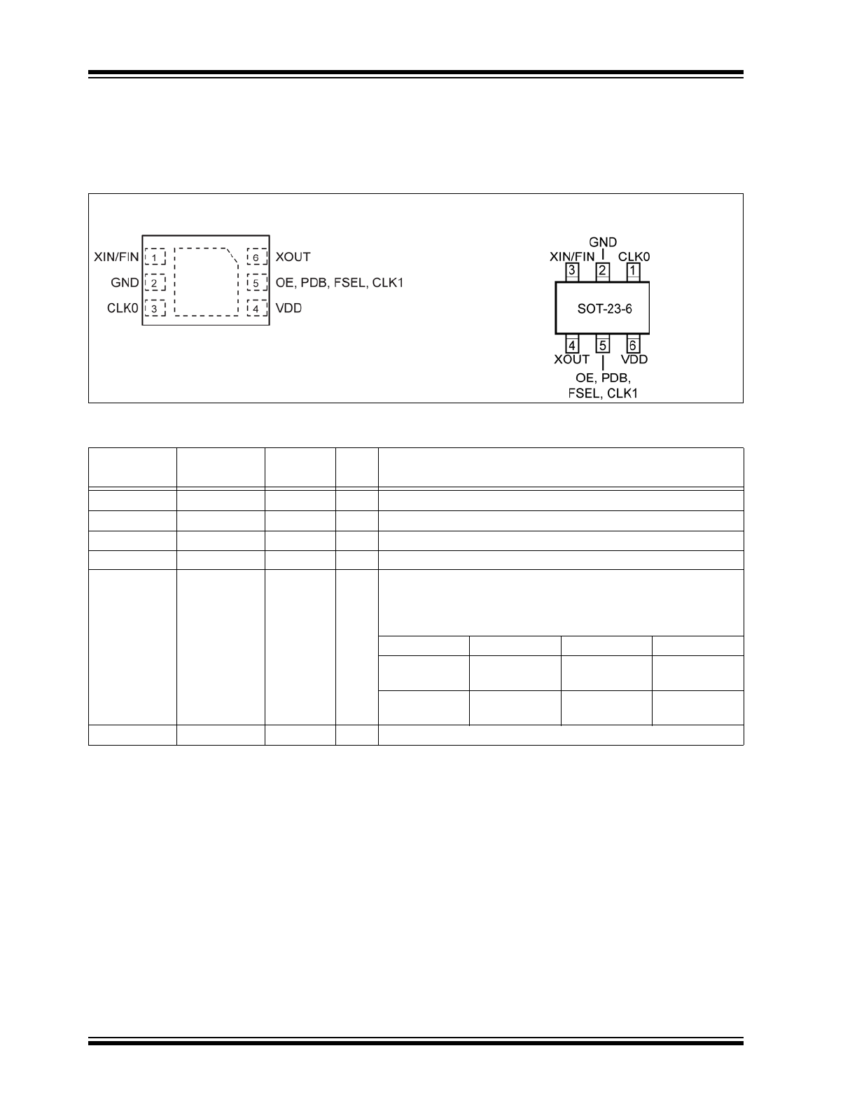
2.0
PIN DESCRIPTIONS
The descriptions of the pins are listed in
Table 2-1
.
Pin Configurations
TABLE 2-1:
PIN FUNCTION TABLE
6-Pin TDFN
Pin Number
6-Pin SOT-23
Pin Number
Name
Type
Description
1
3
XIN, FIN
I
Crystal or reference input pin.
2
2
GND
P
GND connection.
3
1
CLK0
O
Programmable clock output.
4
6
VDD
P
VDD connection.
5
5
OE, PDB,
FSEL,
CLK1
I/O
This programmable I/O pin can be configured as an output
enable (OE) input, power down (PDB) input, frequency select
(FSEL) input, or CLK1 output. This pin has an internal 60 kΩ
pull-up resistor on OE, PDB, and FSEL.
State
OE
PDB
FSEL
0
Tri-State CLK
Power Down
Mode
Bank 0
1 (default)
Operating
Mode
Operating
Mode
Bank 1
6
4
XOUT
O
Crystal output pin. Do not connect if FIN is used.
PL611s-18-xxx
6-Pin TDFN
PL611s-18-xxx
6-Pin SOT-23
2017 Microchip Technology Inc.
DS20005741A-page 7
PL611S-18-XXX
3.0
FUNCTIONAL DESCRIPTION
PL611s-18-xxx is a highly featured, very flexible,
advanced programmable PLL design for high
performance, low-power, small form-factor
applications. The PL611s-18-xxx accepts a crystal
input of 10 MHz to 50 MHz or a reference clock input of
1 MHz to 125 MHz and is capable of producing two
outputs up to 125 MHz. This flexible design allows the
PL611s-18-xxx to deliver any PLL-generated
frequency, F
REF
(Crystal or Ref Clk) frequency or
F
REF
÷ (2 × P) to CLK0 and/or CLK1.
3.1
PLL Programming
The PLL in the PL611s-18-xxx is fully programmable.
The PLL is equipped with a 5-bit input frequency divider
(R-Counter) and an 8-bit VCO frequency feedback loop
divider (M-Counter). The output of the PLL is
transferred to a 14-bit post-VCO divider (P-Counter).
The output frequency is determined by the following
formula:
EQUATION 3-1:
3.2
Clock Output (CLK0)
CLK0 is the main clock output. The PL611s-18-xxx can
also be programmed to provide a second clock output,
CLK1, on the programmable I/O pin (see the
OE/PDB/FSEL/CLK1 field of
Table 2-1
). The output of
CLK0 can be configured as the PLL output (F
VCO
÷ (2
× P)), F
REF
(Ref Clk Frequency) output, or F
REF
÷ (2 ×
P) output. The output drive level can be programmed to
Low Drive (4 mA), Standard Drive (8 mA), or High Drive
(16 mA). The maximum output frequency is 125 MHz.
Because of the long P counter, the minimum output
frequency is as low as 0.5 kHz.
3.3
Clock Output (CLK1)
The CLK1 feature allows the PL611s-18-xxx to have an
additional clock output. This output can be
programmed to one of the following:
• F
REF
• F
REF
÷ 2
• CLK0
• CLK0 ÷ 2
3.4
Output Enable (OE)
The Output Enable feature allows the user to enable
and disable the clock output and PLL by toggling the
OE pin. Because the crystal remains operational when
the output is disabled, the output enable time is much
faster than with the Power Down function. The OE pin
incorporates a 60 kΩ pull up resistor giving a default
condition of logic “1”. Pulling the OE pin low “0” will
tri-state the output buffers.
3.5
Power Down Control (PDB)
The Power Down (PDB) feature allows the user to put
the PL611s-18-xxx into sleep mode. When activated
(logic ‘0’), PDB disables the PLL, the oscillator circuitry,
counters, and all other active circuitry and tri-state the
output buffers. In Power Down mode the IC consumes
<5 µA of power. The PDB pin incorporates a pull-up
resistor giving a default condition of logic “1”.
3.6
Frequency Select (FSEL)
The Frequency Select (FSEL) feature allows the
PL611s-18-xxx to switch between two pre-programmed
outputs allowing the device on-the-fly frequency
switching. The FSEL pin incorporates a 60 kΩ pull-up
resistor giving a default condition of logic “1”.
3.7
Programmable CLoad
The PL611s-18-xxx is equipped with programmable
S-caps to allow the CLoad to be tuned from 8 pF to
12 pF.
F
OUT
F
REF
M
R
P
=
PL611S-18-XXX
DS20005741A-page 8
2017 Microchip Technology Inc.
4.0
LAYOUT RECOMMENDATIONS
The following guidelines are to assist you with a
performance-optimized PCB design.
4.1
Signal Integrity and Termination
Considerations
• Keep traces short.
• Trace = Inductor. With a capacitive load this
creates ringing.
• Long trace = Transmission Line. Without proper
termination, this causes reflections that look like
ringing.
• Design long traces (greater than one inch) as
“striplines” or “microstrips” with defined
impedance.
• Match the trace at one side to avoid reflections
bouncing back and forth.
4.2
Decoupling and Power Supply
Considerations
• Place decoupling capacitors as close as possible
to the V
DD
pin(s) to limit noise from the power
supply.
• Multiple V
DD
pins should be decoupled separately
for best performance.
• The addition of a ferrite bead in series with V
DD
can help prevent noise from other board sources.
• The value of the decoupling capacitor is
frequency-dependent. Typical values to use are
0.1 µF for designs using crystals <50 MHz and
0.01 µF for designs using crystals >50 MHz.
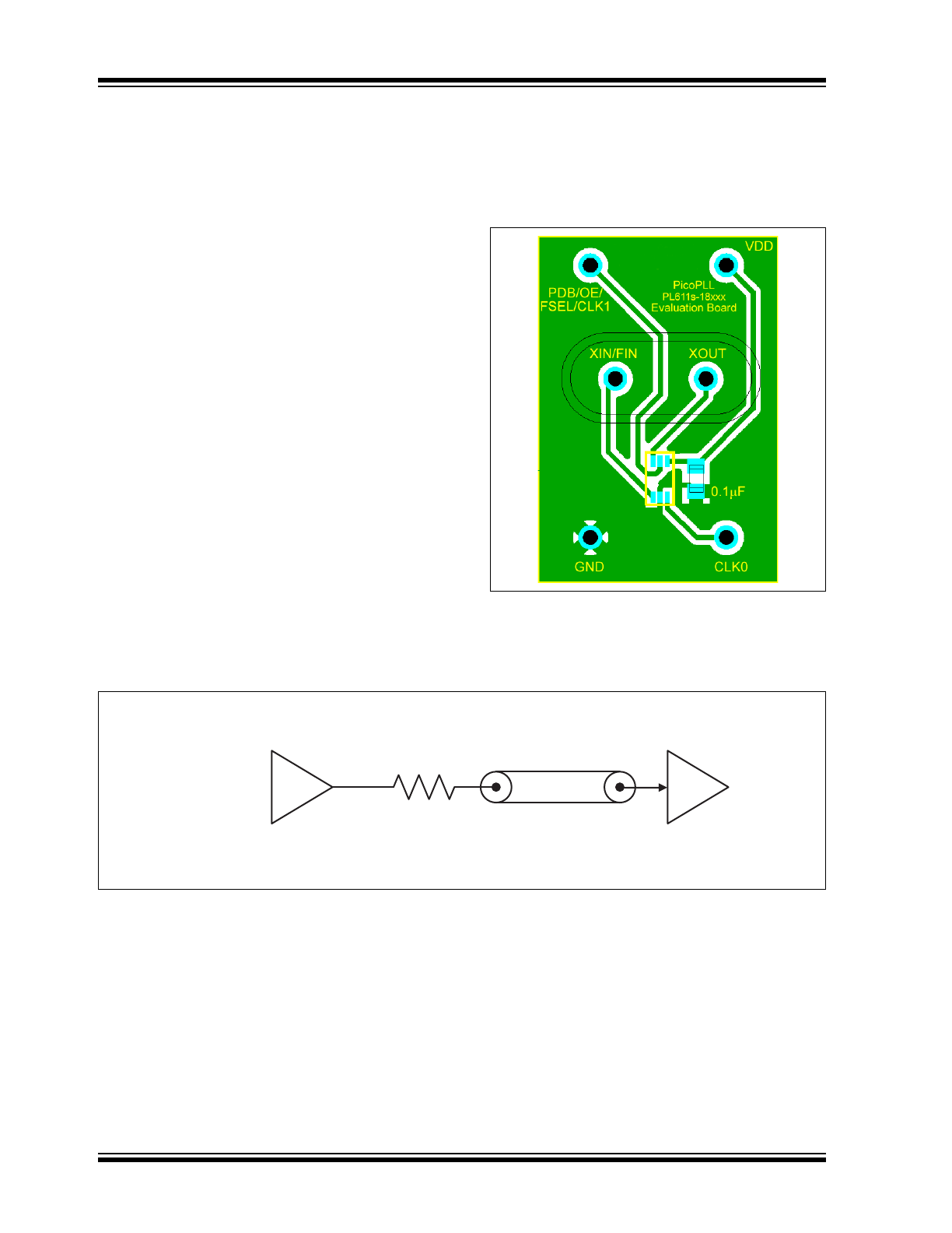
FIGURE 4-1:
TDFN-6L Evaluation Board.
4.3
Typical CMOS Termination
Place series resistor as close as possible to the CMOS output.
FIGURE 4-2:
Typical CMOS Termination.
CMOS Output Buffer
(Typical buffer impedance 20
:
To CMOS Input
Series Resistor
Use value to match output
buffer impedance to 50
:
trace. Typical value 30
:
50
: line
2017 Microchip Technology Inc.
DS20005741A-page 9
PL611S-18-XXX
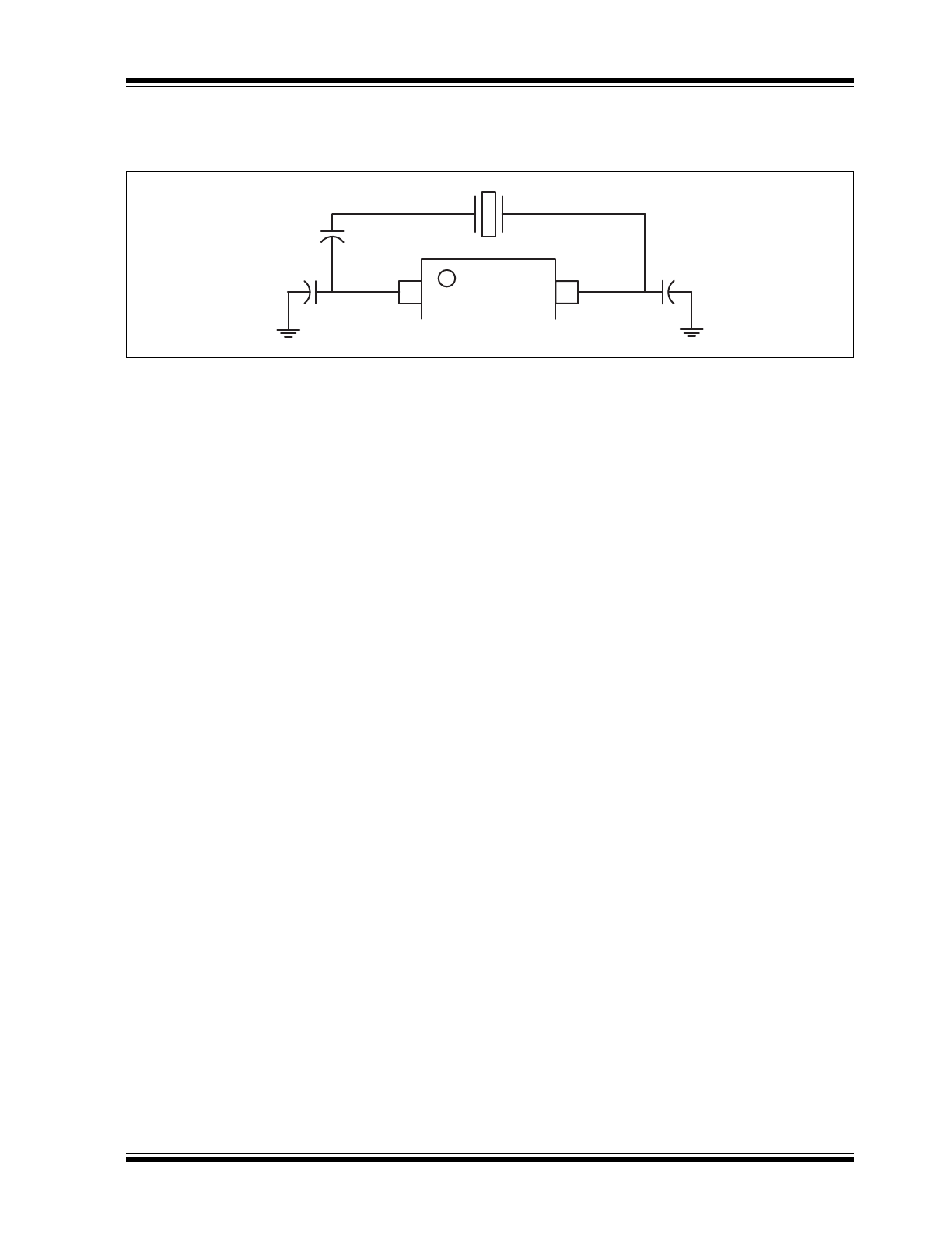
4.4
Crystal Tuning Circuit
Series and parallel capacitors are used to fine tune the crystal load to the circuit load.
CST:
Series capacitor, used to lower circuit load to match crystal load. Raises frequency offset. This can be eliminated
by using a crystal with a CLoad of equal or greater value than the oscillator.
CPT:
Parallel capacitors, used to raise the circuit load to match the crystal load. Lowers frequency offset.
XIN
XOUT
Cpt
Cpt
Cst
PL611S-18-XXX
DS20005741A-page 10
2017 Microchip Technology Inc.
5.0
PACKAGING INFORMATION
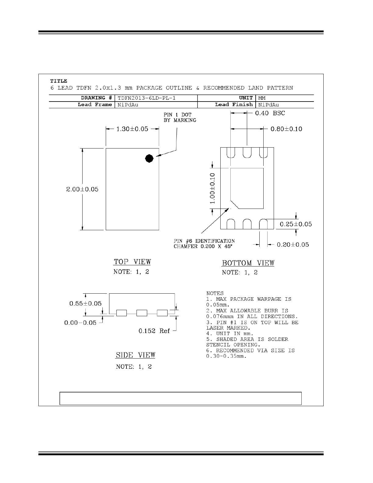
6-Pin TDFN 2.0 mm x 1.3 mm Package Outline and Recommended Land Pattern
Note: For the most current package drawings, please see the Microchip Packaging Specification located at
http://www.microchip.com/packaging.