
_______________General Description
The MAX866 and MAX867 are ultra-small, high-efficiency,
CMOS, step-up, DC-DC switching regulators for 1-cell
battery-powered systems. The MAX866 accepts a posi-
tive input voltage between 0.8V and V
OUT
and converts it
to a higher, pin-selectable output voltage of 3.3V or 5V.
The MAX867 adjustable version accepts 0.8V to 6.0V
input voltages and generates a higher adjustable output
voltage in the 2.7V to 6.0V range. Typical efficiencies are
greater than 80%. Typical no-load supply current is
100µA (1µA in shutdown).
The MAX866/MAX867 combine ultra-low quiescent sup-
ply current and high efficiency to give maximum battery
life. Its high switching frequency permits the use of
small, low-cost inductors and capacitors. Additionally,
internal peak-current limiting protects the IC.
________________________Applications
Pagers
Remote Controls
Detectors
1-Cell Battery-Operated Equipment
Backup Supplies
____________________________Features
♦
0.8V to 6.0V Input Supply Voltage
♦
0.9V Guaranteed Start-Up Supply Voltage
♦
>80% Efficiency Over Wide Load Range
♦
100µA No-Load Battery Current (V
OUT
= 3.3V)
♦
1µA Shutdown Mode
♦
Up to 250kHz Switching Frequency
♦
±1.5% Reference Tolerance
♦
Low-Battery Detector (LBI/LBO)
♦
Ultra-Small 8-Pin µMAX Package (1.11mm high)
♦
Circuit Fits in 0.2in
2
______________Ordering Information
MAX866/MAX867
3.3V/5V or Adjustable-Output,
Single-Cell DC-DC Converters
________________________________________________________________
Maxim Integrated Products
1
1
2
3
4
8
7
6
5
LX
GND
OUT
LBI
LBO
REF
3/5
SHDN
MAX866
µ
MAX
TOP VIEW
1
2
3
4
8
7
6
5
LX
GND
OUT
LBI
LBO
REF
FB
SHDN
MAX867
µ
MAX
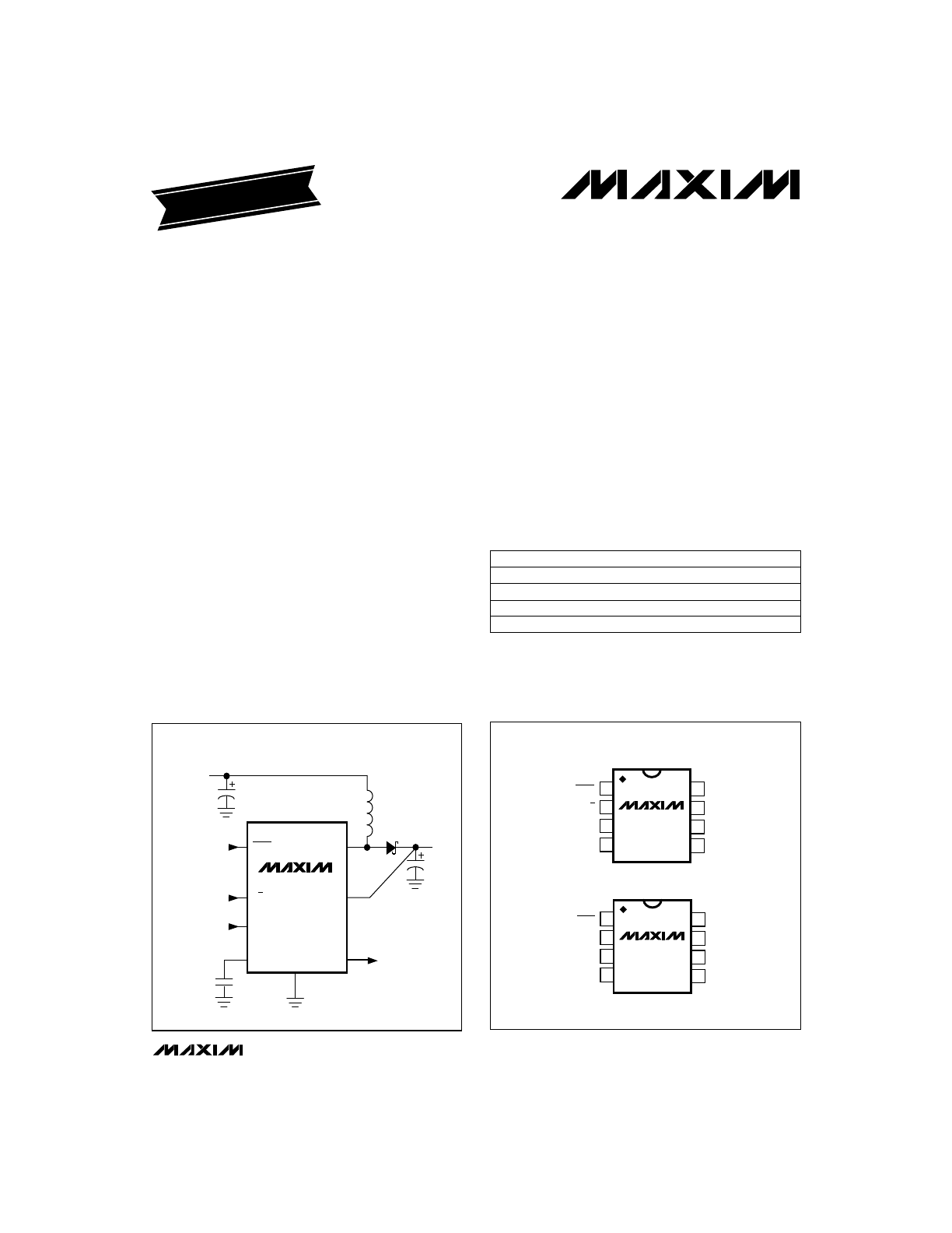
_________________Pin Configurations
MAX866
SHDN
3/5
REF
LX
GND
OUT
INPUT
0.8V TO V
OUT
MBRS0520LTI
OR 1N5817
OUTPUT
5V OR 3.3V
LBO
47
µ
F
0.22
µ
F
330
µ
H
LOW-BATTERY
DETECTOR OUTPUT
ON/OFF
3V/5V SELECT
LBI
LOW-BATTERY
DETECTOR
INPUT
__________Typical Operating Circuit
Call toll free 1-800-998-8800 for free samples or literature.
19-0374; Rev 0; 4/95
PART
TEMP. RANGE PIN-PACKAGE
MAX866
C/D
0°C to +70°C
Dice*
MAX866EUA
-40°C to +85°C
8 µMAX
MAX867
C/D
0°C to +70°C
Dice*
MAX867EUA
-40°C to +85°C
8 µMAX
* Dice are tested at T
A
= +25°C only.
EVALUATION KIT
MANUAL AVAILABLE
V
MAX866/MAX867
3.3V/5V or Adjustable-Output,
Single-Cell DC-DC Converters
2
_______________________________________________________________________________________
ABSOLUTE MAXIMUM RATINGS
ELECTRICAL CHARACTERISTICS
(Circuit of Figure 2, V
IN
= 1.2V, I
LOAD
= 0mA, T
A
= +25°C, unless otherwise noted.)
Stresses beyond those listed under “Absolute Maximum Ratings” may cause permanent damage to the device. These are stress ratings only, and functional
operation of the device at these or any other conditions beyond those indicated in the operational sections of the specifications is not implied. Exposure to
absolute maximum rating conditions for extended periods may affect device reliability.
Supply Voltage (OUT to GND) ...................................-0.3V, +7V
Switch Voltage (LX to GND) .......................................-0.3V, +7V
S
—
H
—
D
—
N
–
, LBO to GND ....................................................-0.3V, +7V
LBI, REF, 3/
–
5
–
, FB to GND ............................-0.3V, (V
OUT
+ 0.3V)
Reference Current (I
REF
) ..................................................2.5mA
Continuous Power Dissipation (T
A
= +70°C)
µMAX (derate 4.1mW/°C above +70°C) ......................330mW
Reverse Battery Current (T
A
≤
+45°C) (Note 1) ................750mA
Operating Temperature Ranges
MAX86_C/D .......................................................0°C to +70°C
MAX86_EUA ...................................................-40°C to +85°C
Junction Temperature .....................................................+150°C
Storage Temperature Range ............................-65°C to +160°C
Lead Temperature (soldering, 10sec) ............................+300°C
Note 1:
Reverse battery current is measured from the
Typical Operating Circuit’s battery input terminal to GND when the battery is
connected backwards. A reverse current of 750mA will not exceed the package dissipation limits but, if left for an extended
time (more than ten minutes), may degrade performance.
With falling edge
3/
–
5
–
= 3V, -20µA
≤
REF load
≤
250µA, C
REF
= 0.22µF
No REF load
0.9V
≤
V
IN
≤
3V
I
LOAD
= 0mA, 3/
–
5
–
= 3V, LBI = 1.5V,
V
OUT
= 3.47V, FB = 1.5V
CONDITIONS
V
1.22
1.25
1.28
LBI Input Threshold
%
0.8
2.0
Reference Load Regulation
V
1.22
1.25
1.28
Reference Voltage
mA
500
µA
1
Shutdown Quiescent Current
(Note 4)
µA
27
60
Quiescent Supply Current in
3.3V mode (Note 4)
4.80
5.0
5.20
3.17
3.3
3.43
4.80
5.0
5.20
4.75
5.0
5.25
3.13
3.3
3.47
4.75
5.0
5.25
Output Voltage
(Note 2)
UNITS
MIN
TYP
MAX
PARAMETER
Peak Inductor Current Limit
MAX866, 3/
–
5
–
= 0V, 0mA
≤
I
LOAD
≤
6mA
MAX866, 3/
–
5
–
= 3V, 0mA
≤
I
LOAD
≤
8mA
MAX867, V
OUT
= 5V, 0mA
≤
I
LOAD
≤
6mA
MAX866, 3/
–
5
–
= 0V, 0mA
≤
I
LOAD
≤
6mA
MAX866, 3/
–
5
–
= 3V, 0mA
≤
I
LOAD
≤
8mA
MAX867, V
OUT
= 5V, 0mA
≤
I
LOAD
≤
6mA
S
—
H
—
D
—
N
–
= 0V, 3/
–
5
–
= 3V, LBI = 1.5V, V
OUT
= 3.47V,
FB = 1.5V
0.9V
≤
V
IN
≤
3V
MAX866, 3/
–
5
–
= 0V, 4.8V
≤
V
LOAD
≤
5.2V
MAX866, 3/
–
5
–
= 3V, 3.17V
≤
V
LOAD
≤
3.43V
MAX867, V
OUT
= 5V, 4.8V
≤
V
LOAD
≤
5.2V
MAX866, 3/
–
5
–
= 0V, 4.8V
≤
V
LOAD
≤
5.2V
MAX866, 3/
–
5
–
= 3V, 3.17V
≤
V
LOAD
≤
3.43V
MAX867, V
OUT
= 5V, 4.8V
≤
V
LOAD
≤
5.2V
6
9
8
13
6
9
10
15
15
23
mA
10
15
Maximum Load Current
(Note 2)
0.9V
≤
V
IN
≤
3V,
T
A =
T
MIN TO
T
MAX
(Note 3)
1.2V
≤
V
IN
≤
3V
V
0.8
0.9
Minimum Start-Up
Supply Voltage
Output set for 3.3V, measured at V
IN
in Figure 2, V
IN
= 1.5V
µA
100
No-Load Battery Current
1.2V
≤
V
IN
≤
3V
MAX866, 3/
–
5
–
= 0V, 0mA
≤
I
LOAD
≤
10mA
MAX866, 3/
–
5
–
= 3V, 0mA
≤
I
LOAD
≤
15mA
MAX867, V
OUT
= 5V, 0mA
≤
I
LOAD
≤
10mA
4.80
5.0
5.20
3.17
3.3
3.43
4.80
5.0
5.20
MAX866/MAX867
3.3V/5V or Adjustable-Output,
Single-Cell DC-DC Converters
_______________________________________________________________________________________
3
100
0
10
0.01
0.1
1
10
100
1000
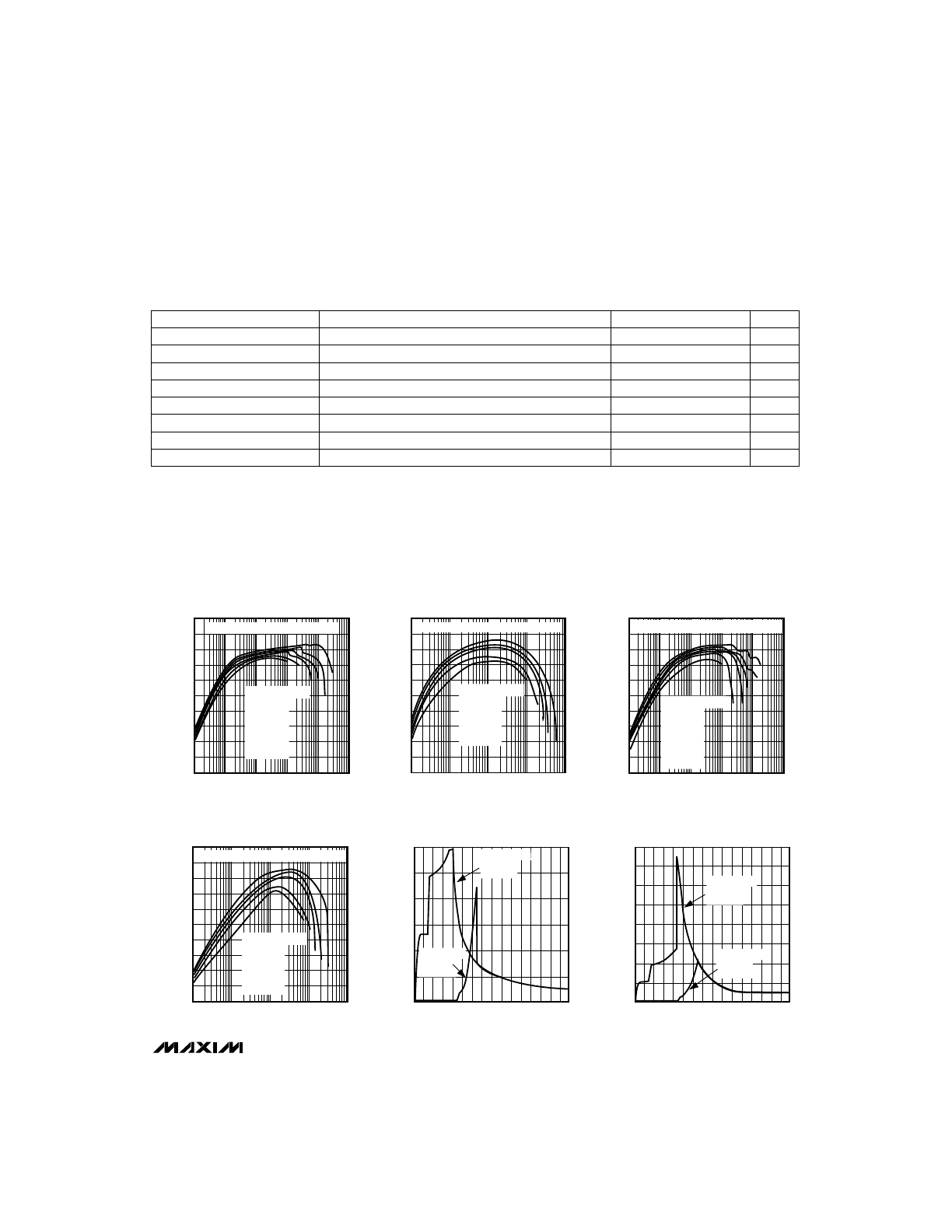
EFFICIENCY vs. LOAD CURRENT (V
OUT
= 3.3V)
30
20
MAX866/667-01
LOAD CURRENT (mA)
EFFICIENCY (%)
40
50
60
70
80
90
TOP TO BOTTOM:
V
IN
= 2.0V
V
IN
= 1.5V
V
IN
= 1.25V
V
IN
= 1.0V
V
IN
= 0.75V
V
IN
= 0.5V
L = SUMIDA CD73-331 (330
µ
H, 1.5
Ω
)
100
90
0
0.01
1
0.1
10
100
EFFICIENCY vs. LOAD CURRENT (V
OUT
= 5.0V)
20
MAX866/67-04
LOAD CURRENT (mA)
EFFICIENCY (%)
40
60
80
70
50
30
10
TOP TO BOTTOM:
V
IN
= 2.0V
V
IN
= 1.5V
V
IN
= 1.25V
V
IN
= 1.0V
V
IN
= 0.75V
L = COILCRAFT D01608-334 (330
µ
H, 2.9
Ω
)
100
90
0
0.01
1
0.1
10
100
EFFICIENCY vs. LOAD CURRENT (V
OUT
= 3.3V)
20
MAX866/67-02
LOAD CURRENT (mA)
EFFICIENCY (%)
40
60
80
70
50
30
10
TOP TO BOTTOM:
V
IN
= 2.0V
V
IN
= 1.5V
V
IN
= 1.25V
V
IN
= 1.0V
V
IN
= 0.75V
L = COILCRAFT D01608-334 (330
µ
H, 2.9
Ω
)
100
0
10
0.01
0.1
1
10
100
1000
EFFICIENCY vs. LOAD CURRENT (V
OUT
= 5.0V)
30
20
MAX866/667-03
LOAD CURRENT (mA)
EFFICIENCY (%)
40
50
60
70
80
90
TOP TO BOTTOM:
V
IN
= 2.0V
V
IN
= 1.5V
V
IN
= 1.25V
V
IN
= 1.0V
V
IN
= 0.75V
V
IN
= 0.5V
L = SUMIDA CD73-331 (330
µ
H, 1.5
Ω
)
1200
0
0
0.2
0.4
0.6
0.8 1.0
1.2
1.4 1.6
NO-LOAD BATTERY CURRENT
vs. BATTERY VOLTAGE (V
OUT
= 3.3V)
400
200
1000
MAX866/67-05
BATTERY VOLTAGE (V)
BATTERY CURRENT (
µ
A)
800
600
DECREASING
BATTERY
VOLTAGE
INCREASING
BATTERY
VOLTAGE
4000
0
0
0.2
0.4
0.6
0.8 1.0
1.2
1.4 1.6
NO-LOAD BATTERY CURRENT
vs. BATTERY VOLTAGE (V
OUT
= 5V)
1000
500
3500
MAX866/67-06
BATTERY VOLTAGE (V)
BATTERY CURRENT (
µ
A)
2000
2500
3000
1500
DECREASING
BATTERY
VOLTAGE
INCREASING
BATTERY
VOLTAGE
__________________________________________Typical Operating Characteristics
(Circuits of Figure 2, T
A
= +25°C, unless otherwise noted.)
ELECTRICAL CHARACTERISTICS (continued)
(Circuit of Figure 2, V
IN
= 1.2V, I
LOAD
= 0mA, T
A
= +25°C, unless otherwise noted.)
Note 2:
Output current specified with circuit of Figure 2 and CoilCraft D01608-334 inductor for test purposes only. More (or less)
output current can be supplied with other coil types depending on inductance value and coil resistance. See
Typical Operating
Characteristics for other coil types. Output voltage and output current are guaranteed over this V
IN
operating range once the
device has started up. Actual V
IN
start-up voltage depends on load current.
Note 3:
Output voltage specifications over temperature are guaranteed by design to limits that are 6 sigma from either side of the mean.
Note 4:
Current measured into OUT. V
OUT
is forced to 3.47V to maintain LX off when measuring device current.
PARAMETER
CONDITIONS
MIN
TYP
MAX
UNITS
S
—
H
—
D
—
N
–
, 3/
–
5
–
Input Voltage High
0.32 x V
OUT
V
S
—
H
—
D
—
N
–
, 3/
–
5
–
, FB, LBI Input Current
LBI = 1.5V, FB = 1.5V,
–
S
—
H
—
D
—
N
–
= 0V or 3V, 3/
–
5
–
= 0V or 3V
±40
±100
nA
FB Voltage
MAX867, output in regulation
1.22
1.25
1.28
V
Output Voltage Range
MAX867
2.7
6.0
V
–
S
—
H
—
D
—
N
–
, 3/
–
5
–
Input Voltage Low
0.08 x V
OUT
V
LBO Output Leakage Current
LBO = 5V
1
µA
LBI Input Hysteresis
25
mV
LBO Output Voltage Low
I
SINK
= 2mA, open-drain output
0.4
V
MAX866/MAX867
3.3V/5V or Adjustable-Output,
Single-Cell DC-DC Converters
4
_______________________________________________________________________________________
____________________________Typical Operating Characteristics (continued)
(Circuits of Figure 2, T
A
= +25°C, unless otherwise noted.)
1.5
1.4
1.3
1.2
1.1
1.0
0.8
0.5
0.1
1
100
START-UP INPUT VOLTAGE vs. LOAD CURRENT
(V
OUT
= 3.3V)
0.7
0.6
0.9
MAX186-14A
MAX866/67-07
LOAD CURRENT (mA)
START-UP INPUT VOLTAGE (V)
10
100µH
47µH
220µH
330µH
1mH
1.5
1.4
1.3
1.2
1.1
1.0
0.8
0.5
0.1
1
100
START-UP INPUT VOLTAGE vs. LOAD CURRENT
(V
OUT
= 5V)
0.7
0.6
0.9
MAX186-14A
LOAD CURRENT (mA)
START-UP INPUT VOLTAGE (V)
10
100µH
47µH
220µH
330µH
MAX866/67-08
1
10
1000
INPUT VOLTAGE vs. LOAD CURRENT
(V
OUT
= 3.3V)
MAX186-14A
MAX866/67-09
LOAD CURRENT (mA)
INPUT VOLTAGE (V)
100
100µH
47µH
22µH
330µH
1mH
3.0
2.5
1.5
0
1.0
0.5
2.0
1
10
1000
INPUT VOLTAGE vs. LOAD CURRENT
(V
OUT
= 5V)
MAX186-14A
MAX866/67-10
LOAD CURRENT (mA)
INPUT VOLTAGE (V)
3.0
2.5
1.5
0
1.0
0.5
2.0
100
22µH
330µH
47µH
100µH
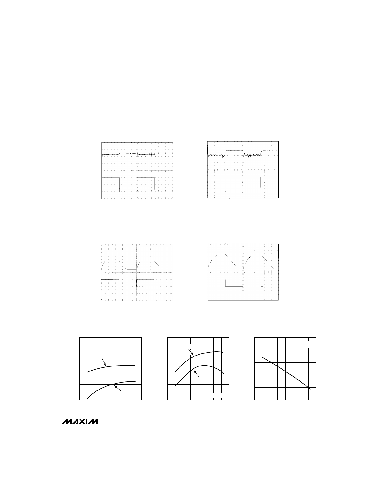
A: 3.3V OUTPUT VOLTAGE, AC COUPLED 20mV/div
B: INPUT VOLTAGE (0.9V AND 1.4V) 500mV/div
I
LOAD
= 10mA, C
OUT
= 47
µ
F
MAX866 LINE-TRANSIENT RESPONSE
(3.3V MODE)
1ms/div
A
B
5
0
REFERENCE VOLTAGE
vs. REFERENCE CURRENT
6
10
MAX866/67-11
REFERENCE LOAD CURRENT (
µ
A)
V
REF
LOAD REGULATION (mV)
8
7
100
200
9
50
150
250
4
3
2
1
0
A: 5.0V OUTPUT VOLTAGE, AC COUPLED 20mV/div
B: INPUT VOLTAGE (0.9V AND 1.4V) 500mV/div
I
LOAD
= 10mA, C
OUT
= 47
µ
F
MAX866 LINE-TRANSIENT RESPONSE
(5V MODE)
1ms/div
A
B
MAX866/MAX867
3.3V/5V or Adjustable-Output,
Single-Cell DC-DC Converters
_______________________________________________________________________________________
5
A: 5.0V OUTPUT VOLTAGE, AC COUPLED 20mV/div
B: OUTPUT CURRENT (0mA AND 10mA) 5mV/div
(TEKTRONIX P6042 CURRENT PROBE)
I
LOAD
= 5mA, C
OUT
= 47
µ
F, V
IN
= 1.25V
MAX866 LOAD-TRANSIENT RESPONSE
(5V MODE)
1ms/div
A
B
A: 3.3V OUTPUT VOLTAGE, 2V/div
B: SHDN INPUT VOLTAGE (0V AND 5V) 2V/div
I
LOAD
= 10mA
MAX866 SHUTDOWN RESPONSE
(3.3V MODE)
10ms/div
A
B
A: 5.0V OUTPUT VOLTAGE, 2V/div
B: SHDN INPUT VOLTAGE (0V AND 5V) 5V/div
I
LOAD
= 10mA
MAX866 SHUTDOWN RESPONSE
(5V MODE)
10ms/div
A
B
____________________________Typical Operating Characteristics (continued)
(Circuits of Figure 2, T
A
= +25°C, unless otherwise noted.)
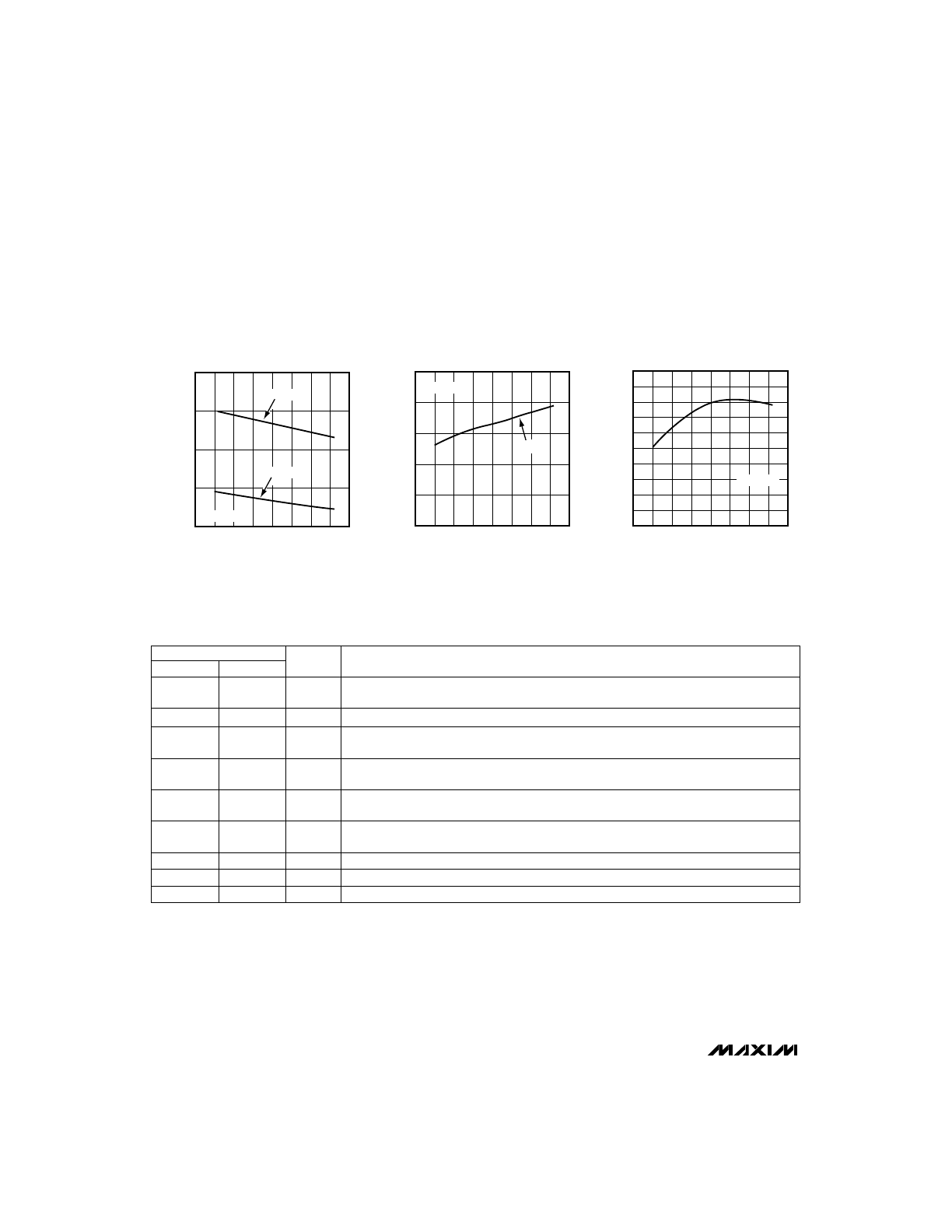
1.250
-60
MAX867 LBI AND FB THRESHOLD
vs. TEMPERATURE
1.260
MAX866/67-24
TEMPERATURE (°C)
LBI, FB VOLTAGE (V)
0
60
-20
-40
20
80
40
100
1.240
LBI
VFB (MAX867)
0
-60
MAX866 OUTPUT VOLTAGE ERROR
vs. TEMPERATURE
0.5
MAX866/67-25
TEMPERATURE (°C)
OUTPUT VOLTAGE ERROR (%)
0
60
-20
-40
20
80
40
100
-0.5
5V MODE
I
LOAD
= OA
3.3V MODE
-60
START-UP VOLTAGE
vs. TEMPERATURE
1.0
0.9
0.8
0.7
0.6
MAX866/67-26
TEMPERATURE (°C)
START-UP VOLTAGE (V)
0
60
-20
-40
20
80
40
100
0.5
I
LOAD
= 0A
A: 3.3V OUTPUT VOLTAGE, AC COUPLED 20mV/div
B: OUTPUT CURRENT (0mA AND 10mA) 5mV/div
(TEKTRONIX P6042 CURRENT PROBE)
I
LOAD
= 5mA, C
OUT
= 47
µ
F, V
IN
= 1.25V
MAX866 LOAD-TRANSIENT RESPONSE
(3.3V MODE)
1ms/div
A
B
MAX866/MAX867
3.3V/5V or Adjustable-Output,
Single-Cell DC-DC Converters
6
_______________________________________________________________________________________
______________________________________________________________Pin Description
N-Channel Power-MOSFET Drain
8
8
Low-Battery Output. An open-drain N-channel MOSFET sinks current when the voltage at
LBI drops below 1.25V.
4
4
Low-Battery Input. When the voltage on LBI drops below 1.25V, LBO sinks current.
If not used, connect to V
IN
.
5
5
Connect OUT to the regulator output. OUT provides bootstrap power to the IC.
6
6
Power Ground. Must be low impedance; solder directly to ground plane.
7
7
1.25V Reference Voltage Output. Bypass with 0.22µF to GND (0.1µF if there is no external
reference load). Maximum load capability is 250µA source, 20µA sink.
3
3
Feedback Input for adjustable-output operation. Connect to an external resistor voltage
divider between OUT and GND.
2
—
Selects the output voltage; connect to GND for 5V output, and to OUT for 3.3V output.
—
2
Shutdown Input. When low, the entire circuit is off and V
OUT
= V
IN
- V
D,
where V
D
is the
forward voltage drop of the external Schottky rectifier.
1
1
FUNCTION
PIN
LX
LBO
LBI
OUT
GND
REF
FB
3/
–
5
–
–
S
—
H
—
D
—
N
–
NAME
MAX866
MAX867
____________________________Typical Operating Characteristics (continued)
(Circuits of Figure 2, T
A
= +25°C, unless otherwise noted.)
24
-60
QUIESCENT SUPPLY CURRENT
vs. TEMPERATURE
30
28
26
22
MAX866/67-28
TEMPERATURE (°C)
QUIESCENT SUPPLY CURRENT (
µ
A)
0
60
-20
-40
20
80
40
100
20
I
OUT
V
OUT
= 3.47V
1.250
-60
REFERENCE VOLTAGE
vs. TEMPERATURE
1.255
MAX866/67-29
TEMPERATURE (°C)
REFERENCE VOLTAGE (V)
0
60
-20
-40
20
80
40
100
1.245
I
REF
= 0A
-60
OUTPUT CURRENT CAPABILITY
vs. TEMPERATURE
30
25
20
15
MAX866/67-27
TEMPERATURE (°C)
OUTPUT CURRENT (mA)
0
60
-20
-40
20
80
40
100
10
V
IN
= 0.9V
3.3V MODE
V
IN
= 1.2V
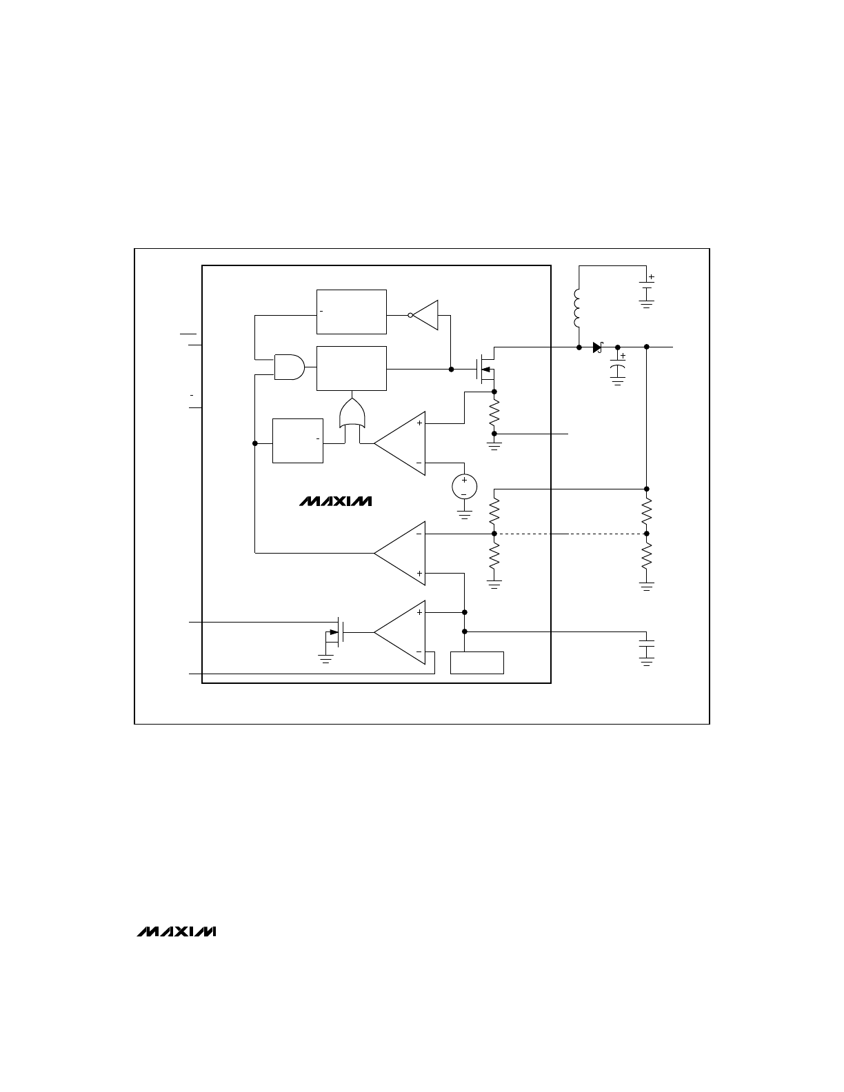
_______________Detailed Description
Operating Principle
The MAX866/MAX867 combine a switch-mode regula-
tor, N-channel power MOSFET, precision voltage refer-
ence, and power-fail detector in a single monolithic
device. The MOSFET is a “sense-FET” type for best effi-
ciency, and has a very low gate threshold voltage to
ensure start-up with low battery voltages (0.8V typ).
PFM Control Scheme
The MAX866/MAX867 control scheme (Figure 1) com-
bines low-voltage efficiency (80% typ) with low battery
drain (100µA typ). There is no oscillator; switching is
accomplished by a pair of one shots that set a maxi-
mum LX on-time (4.5µs typ) and a minimum LX off-time
(1µs). LX on-time will be terminated early if the inductor
current reaches 0.5A before 4.5µs elapses. With the
standard application circuit (Figure 2a), LX current is
typically less than 50mA, so LX on-time is normally not
terminated by the 0.5A limit and lasts the complete
4.5µs. The LX on-resistance is typically 1
Ω
to minimize
switch losses. The MAX866/MAX867 switching frequen-
cy depends on load, input voltage, and inductor value,
and it can range up to 250kHz with typical component
values.
MAX866/MAX867
3.3V/5V or Adjustable-Output,
Single-Cell DC-DC Converters
_______________________________________________________________________________________
7
MAX866/MAX867
SHDN
3/5*
LBO
LBI
N
LBI COMPARATOR
ERROR COMPARATOR
CURRENT-LIMIT
COMPARATOR
ONE-SHOT
TRIG
Q
Q
ONE-SHOT
TRIG
S
Q
R
F/F
MINIMUM
OFF-TIME
ONE-SHOT
V
BATT
LX
N
GND
OUT
V
OUT
**
FB**
**
*
*
REF
REFERENCE
MAXIMUM
ON-TIME
ONE-SHOT
*MAX866 ONLY
**MAX867 ONLY
Figure 1. Block Diagram
MAX866/MAX867
3.3V/5V or Adjustable-Output,
Single-Cell DC-DC Converters
8
_______________________________________________________________________________________
Voltage Reference
The precision voltage reference is suitable for driving
external loads, such as an analog-to-digital converter.
The voltage-reference output changes less than ±2%
when sourcing up to 250µA and sinking up to 20µA. If
the reference drives an external load, bypass it with
0.22µF to GND. If the reference is unloaded, bypass it
with at least 0.1µF.
Logic Inputs and Outputs
The 3/5 input is internally diode clamped to GND and
OUT, and should not be connected to signals outside
this range. The SHDN input and LBO output (open-
drain) are not clamped to V+ and can be pulled as high
as 7V regardless of the voltage at OUT
.
Do not leave
control inputs (3/5, LBI, or SHDN) floating.
__________________Design Procedure
Output Voltage Selection
For the MAX866, you can select a 3.3V or 5V output volt-
age under logic control, or by tying 3/5 to GND or OUT.
The MAX867’s output voltage is set by two resistors, R1
and R2 (Figure 2b), which form a voltage divider
between the output and FB. Use the following equation
to determine the output voltage:
R1 + R2
V
OUT
= V
REF
(
_________
)
R2
where V
REF
= 1.25V.
To simplify resistor selection:
V
OUT
R1 = R2
(
_______ - 1
)
V
REF
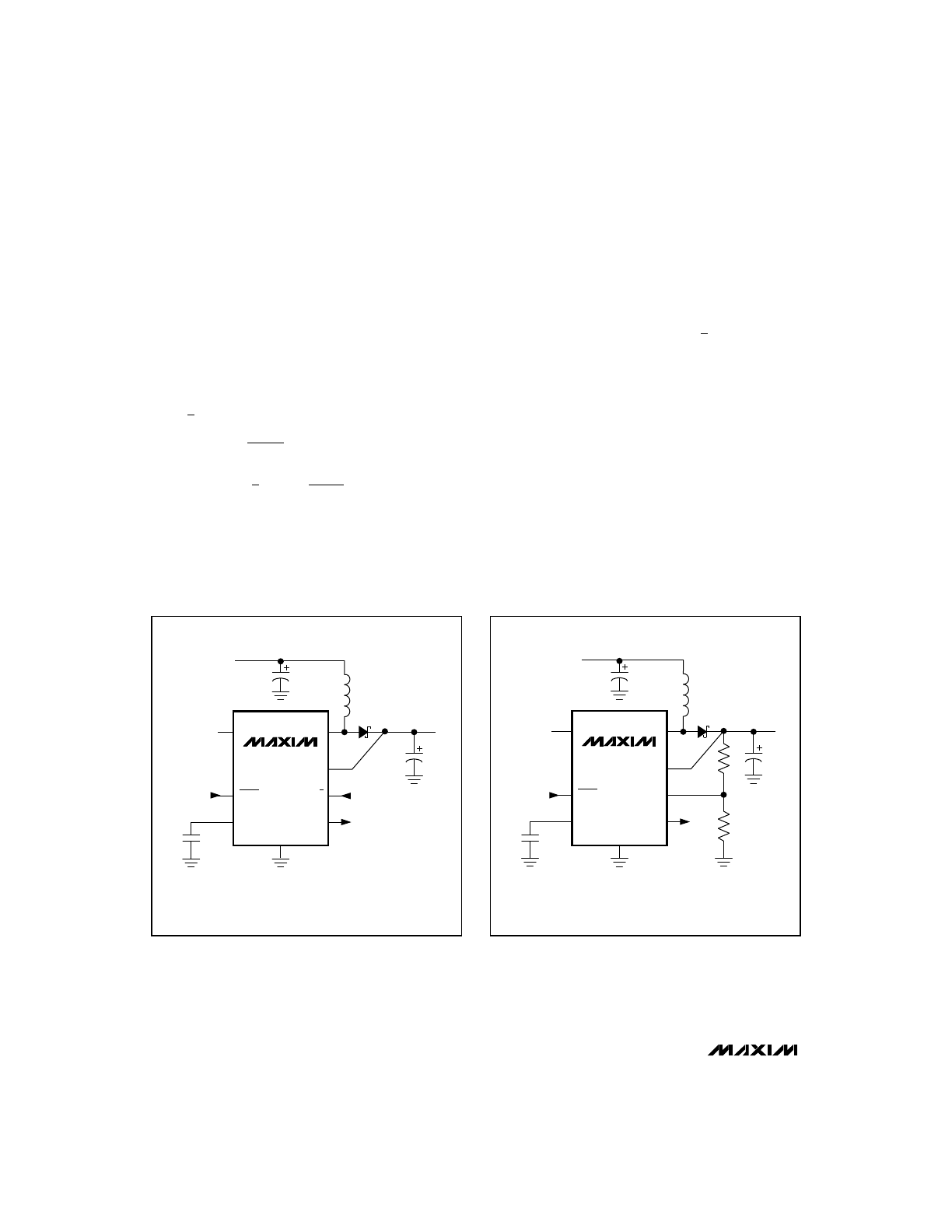
C1
47
µ
F
L1
330
µ
F
V
IN
D1
C2
47
µ
F
R1
R2
LX
OUT
FB
LBO
LBI
REF
SHDN
GND
C3
0.1
µ
F
V
OUT
5
1
3
8
6
2
4
7
MAX867
L1 = COILCRAFT DO1608-334
D1 = MOTOROLA MBR0520LTI
C1
47
µ
F
L1
330
µ
H
V
IN
D1
C2
47
µ
F
R1
LX
OUT
3/5
LBO
LBI
REF
SHDN
GND
C3
0.1
µ
F
V
OUT
5
1
3
8
6
2
4
7
MAX866
L1 = COILCRAFT DO1608-334
OUTPUT
SELECT
D1 = MOTOROLA MBR0520LTI
Figure 2b. Standard Application Circuit—Adjustable Output
Voltage
Figure 2a. Standard Application Circuit—Preset Output
Voltage
MAX866/MAX867
3.3V/5V or Adjustable-Output,
Single-Cell DC-DC Converters
_______________________________________________________________________________________
9
Since the input bias current at FB has a maximum value
of 100nA, large values (10k
Ω
to 300k
Ω
) can be used
for R1 and R2 with no significant accuracy loss. For 1%
error, the current through R1 should be at least 100
times FB’s bias current.
Low-Battery Detection, V
TH
> 1.25V
The MAX866 series contains an on-chip comparator for
low-battery detection. If the voltage at LBI falls below
the regulator’s internal reference voltage (1.25V), LBO
(an open-drain output) sinks current to GND. The low-
battery monitor’s threshold is set by two resistors, R3
and R4 (Figure 3). Set the threshold voltage using the
following equation:
V
TH
R3 = R4
(
____ 1
)
V
REF
where V
TH
is the desired threshold of the low-battery
detector and V
REF
is the internal 1.25V reference.
Since the LBI current is less than 100nA, large resistor
values (typically 10k
Ω
to 300k
Ω
) can be used for R3
and R4 to minimize loading of the input supply.
When the voltage at LBI is below the internal threshold,
LBO sinks current to GND. Connect a pull-up resistor of
100k
Ω
or more from LBO to OUT when driving CMOS
circuits. When LBI is above the threshold, the LBO out-
put is off. If the low-battery comparator is not used,
connect LBI to V
IN
and leave LBO open.
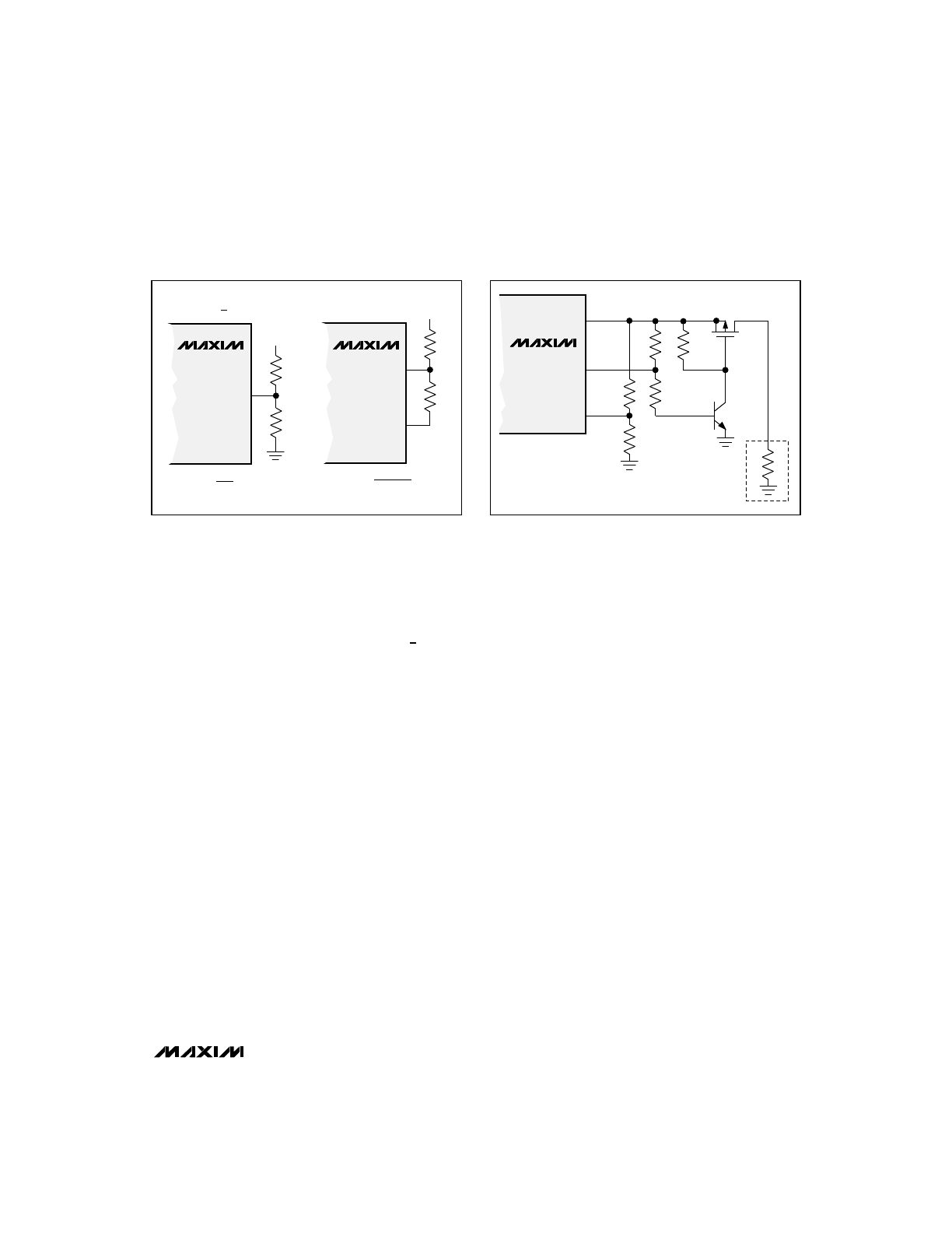
Low-Battery Detection, V
TH
< 1.25V
When the low-battery detection threshold voltage is
below 1.25V, use the circuit shown on the right in
Figure 3. This circuit uses V
OUT
(3.3V or 5.0V in the
MAX866, adjustable in MAX867) as a reference. The
voltage divider formed by R5 and R6 allows the effec-
tive trip point of V
IN
to be set below 1.25V. R6 is usually
set to approximately 100k
Ω
, and R5 is given by the
formula:
R5 = [R6 x (V
REF
- V
TH
)] / (V
OUT
- V
REF
)
Note that LBI drops below the 1.25V LBI threshold trip
point when either V
IN
or V
OUT
is low.
Since V
OUT
regulation and the LBI threshold are derived
from the same internal voltage reference, they track
together over temperature.
Low-Battery Start-Up
The MAX866/MAX867 are bootstrapped circuits; they
can start under no-load conditions at much lower bat-
tery voltages than under full load. Once started, the out-
put can maintain a moderate load as the battery volt-
age decreases below the start-up voltage (see
Typical
Operating Characteristics). The circuit shown in Figure
4 allows the circuit to start with no load, then uses the
LBI circuit and an external low-threshold P-channel
MOSFET switch to apply the load after the output has
started.
Resistors R7 and R8 are selected to trip the LBI detec-
tor at about 90% of the output voltage. On start-up, LBI
and LBO are low, Q2 is off, and transistor Q1’s gate is
held high by R11. This disconnects the load, allowing
the MAX866 to bootstrap itself at the lowest possible
voltage. When the output reaches its final output volt-
age, LBI and LBO go high, turning on Q2, Q1, and the
load.
Figure 3. Low-Battery Detector Circuits
Figure 4. Low-Voltage Start-Up Circuit
MAX866
LBI
OUT
5
6
R6
R5
V
IN
MAX866
LBI
5
R4
R3
V
IN
FOR V
TH
> 1.25V
R3 = R4
-1
WHERE V
TH
= THE V
IN
TRIP THRESHOLD
WHERE V
TH
= THE V
IN
TRIP THRESHOLD
FOR V
TH
< 1.25V
V
TH
V
REF
(
)
R5 = R6
V
REF
- V
TH
V
OUT
- V
REF
(
)
MAX866
OUT
LBO
LBI
6
4
5
R11
1M
R9
1M
R10
1M
R8
1M
R7
V
OUT
(3.3V/5V)
Q1
MMDFZP02E
Q2
2N3904
(1.25V)
LOAD
MAX866/MAX867
3.3V/5V or Adjustable-Output,
Single-Cell DC-DC Converters
10
______________________________________________________________________________________
Inductor Selection
An inductor value of 330µH works well in most applica-
tions, supplying loads over 10mA and allowing typical
start-up voltages of 0.8V. The inductor value is not
critical, and the MAX866/MAX867 can operate with val-
ues from 22µH to 1mH. In general, smaller inductor val-
ues supply more output current while larger values start
with lower input voltage. Several inductor suppliers and
part numbers are listed in Tables 1 and 2.
The peak inductor current should not exceed the induc-
tor’s current rating. Since the MAX866/MAX867 current
limit of 0.5A will not be reached in most applications,
the peak coil current (I
PK
) is:
I
PK
= (V
IN(max)
x 4.5µs) / L
For a typical 1-cell alkaline design, V
IN(max)
is 1.55V,
so:
I
PK
= (1.55V x 4.5µs) / 330µH = 21.14mA
which is well within the ratings of most surface-mount
coils. Higher efficiency and output current are achieved
with lower inductor resistance, but unfortunately this is
inversely related to physical size. Table 2 indicates
resistance and height for each coil. Some of the small-
est coils have resistances over 10
Ω
, and will not pro-
vide the same output power or efficiency of a 1
Ω
coil.
At light loads however (below 5mA), the efficiency dif-
ferences between low- and high-resistance coils may
be only a percent or two. The
Typical Operating
Characteristics graphs show efficiency and output cur-
rent plots for 1.5
Ω
and 2.9
Ω
, 330µH coils.
Capacitor Selection
A 47µF, 6V, 0.85
Ω
, surface-mount tantalum (SMT)
output filter capacitor typically provides 15mV output
ripple when stepping up from 0.9V to 1.4V at 10mA.
Smaller capacitors (down to 10µF with higher ESRs) are
acceptable for light loads or in applications that can
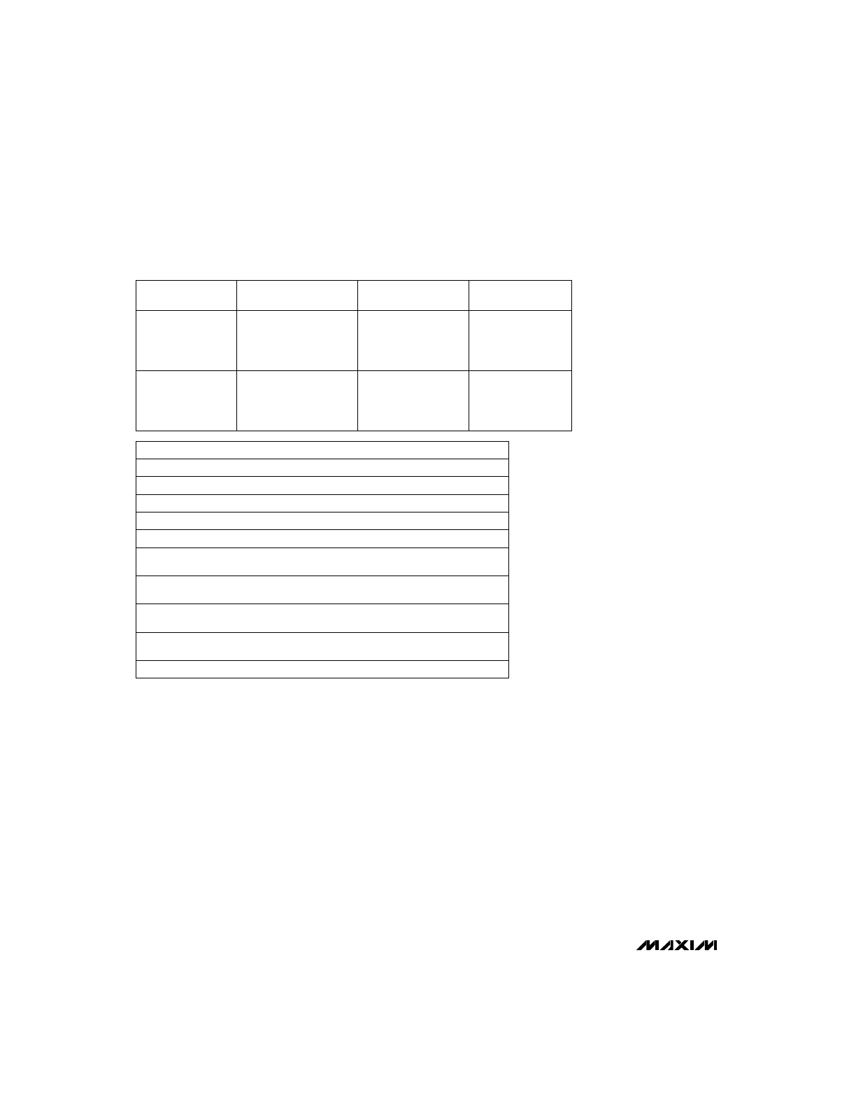
Table 1. Component Suppliers
(708) 803-6294
03-3278-5358
USA:
(708) 803-6100
Japan: 03-3278-5111
TDK
(805) 867-2556
81-3-3494-7414
USA:
(805) 867-2555
Japan: 81-3-3494-7411
Nihon
(708) 639-1469
USA:
(708) 639-6400
CoilCraft
(310) 515-1962
USA:
(310) 515-1720
J.W. Miller
(708) 956-0702
81-3-3607-5144
USA:
(708) 956-0666
Japan: 81-3-3607-5111
Sumida
(619) 661-1055
81-7-2070-1174
USA:
(619) 661-6835
Japan: 81-7-2070-6306
Sanyo
(814) 238-0490
USA:
(800) 831-9172
Murata-Erie
(602) 244-4015
USA:
(602) 244-5303
Motorola
(714) 960-6492
USA:
(714) 969-2491
Matsuo
(207) 283-1941
USA:
(207) 282-5111
AVX
FAX
PHONE
COMPANY
PRODUCTION
METHOD
INDUCTORS
CAPACITORS
Surface Mount
See Table 2
Matsuo 267 series
Sprague 595D series
AVX TPS series
Motorola MBR 0530
Nihon EC15QS02L
Miniature
Through Hole
Sumida
RCH654-220
Sanyo
OS-CON series
low-ESR organic
semiconductor
Motorola 1N5017
RECTIFIERS
tolerate higher output ripple. Values in the 10µF to 47µF
range are recommended.
The equivalent series resistance (ESR) of both bypass
and filter capacitors affects efficiency and output ripple.
Use low-ESR capacitors for best performance, or con-
nect two or more filter capacitors in parallel. Low-ESR,
SMT tantalum capacitors are currently available from
Sprague (595D series) and AVX (TPS series). See
Table 1 for a list of suggested capacitor suppliers.
Rectifier Diode
For optimum performance, a switching Schottky diode
(such as the 1N5817 or MBR0520LTI) is recommended.
Refer to Table 1 for a list of component suppliers. For
low output power applications, a PN-junction switching
diode (such as the 1N4148) will also work well,
although its greater forward voltage drop will reduce
efficiency and raise the start-up voltage.
PC Layout and Grounding
The circuit’s high-frequency operation makes PC layout
important for minimizing ground bounce and noise.
Keep the IC’s GND pin and the ground leads of C1 and
C2 (Figure 2) less than 0.2in (5mm) apart. Also keep all
connections to the FB and LX pins as short as possible.
To maximize output power and efficiency and minimize
output ripple voltage, use a ground plane and solder
the IC’s GND (pin 7) directly to the ground plane.
MAX866/MAX867
3.3V/5V or Adjustable-Output,
Single-Cell DC-DC Converters
______________________________________________________________________________________
11
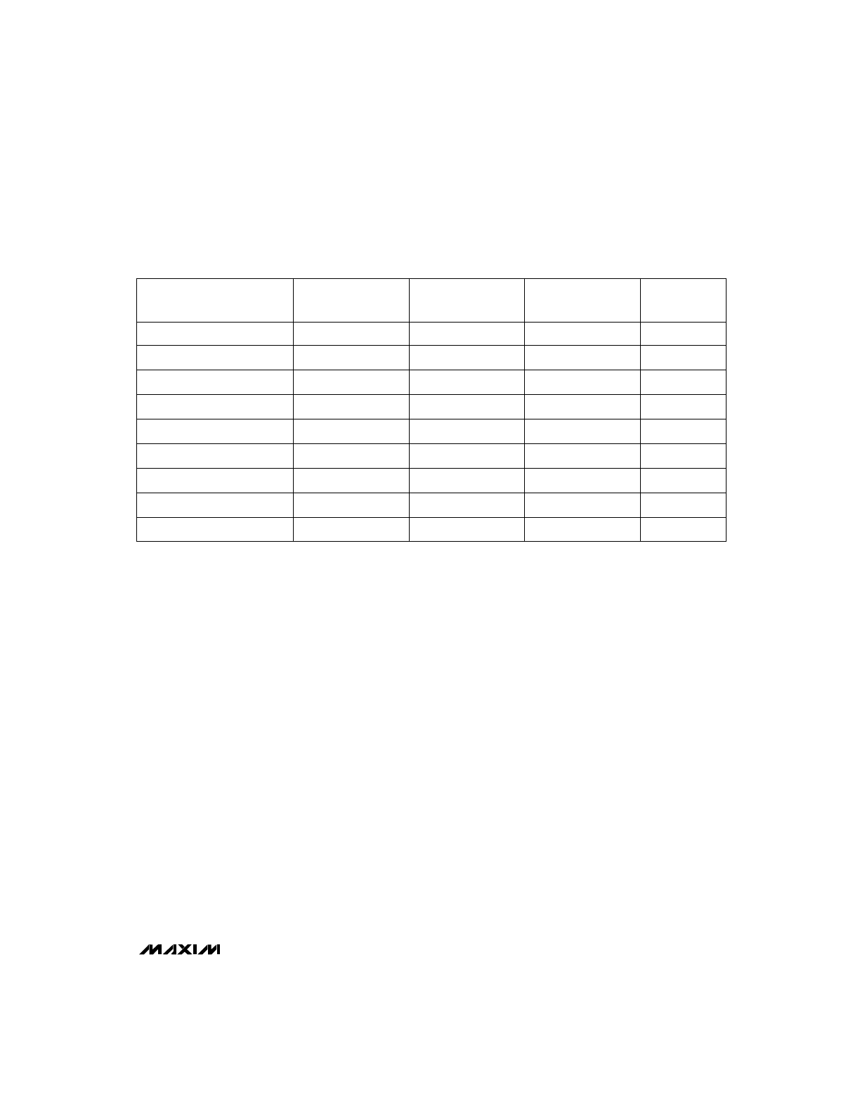
Table 2. Surface-Mount Inductor Information
MANUFACTURER PART
INDUCTANCE
(
m
H)
RESISTANCE
(
W
)
RATED CURRENT
(A)
HEIGHT
(mm)
Sumida CD73-331
330
1.5
0.28
3.5
Sumida CD104-331
330
1.1
0.42
4
Murata-Erie LQH4N331K04M00**
330
8.2
0.095
2.6
TDK NLC565050T-331K**
330
4.9
0.14
5
CoilCraft D01608-334
330
2.9
0.16
3.2
CoilCraft DT1608-334
330*
2.9
0.16
3.2
CoilCraft D03316-334
330
0.7
0.6
5.4
CoilCraft DT3316-334
330*
0.7
0.6
5.4
J.W. Miller PM105-331K
330
1.1
0.52
5.4
* Shielded
** Low cost
Maxim cannot assume responsibility for use of any circuitry other than circuitry entirely embodied in a Maxim product. No circuit patent licenses are
implied. Maxim reserves the right to change the circuitry and specifications without notice at any time.
12
__________________Maxim Integrated Products, 120 San Gabriel Drive, Sunnyvale, CA 94086 (408) 737-7600
© 1995 Maxim Integrated Products
Printed USA
is a registered trademark of Maxim Integrated Products.
MAX866/MAX867
3.3V/5V or Adjustable-Output,
Single-Cell DC-DC Converters
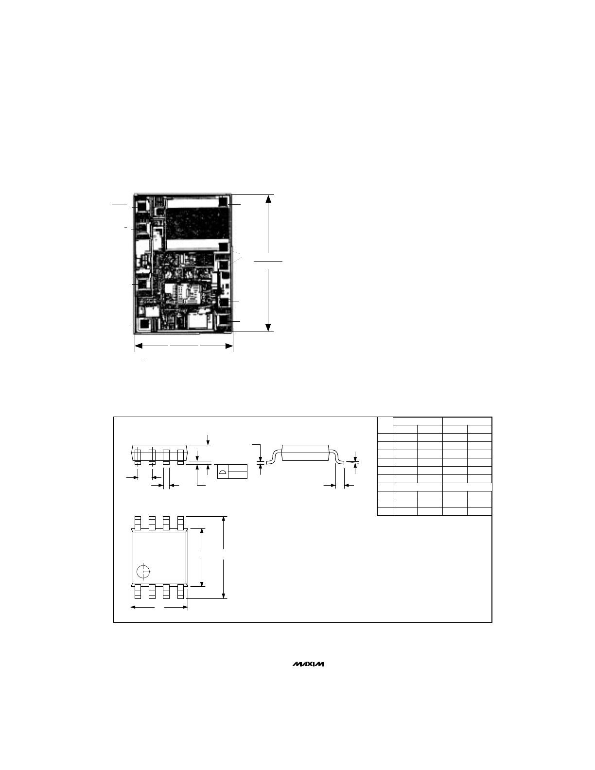
________________________________________________________Package Information
L
α
C
A1
B
DIM
A
A1
B
C
D
E
e
H
L
α
MIN
0.036
0.004
0.010
0.005
0.116
0.116
0.188
0.016
0°
MAX
0.044
0.008
0.014
0.007
0.120
0.120
0.198
0.026
6°
MIN
0.91
0.10
0.25
0.13
2.95
2.95
4.78
0.41
0°
MAX
1.11
0.20
0.36
0.18
3.05
3.05
5.03
0.66
6°
INCHES
MILLIMETERS
8-PIN
µ
MAX
MICROMAX SMALL OUTLINE
PACKAGE
0.65
0.0256
A
e
E
H
D
0.101mm
0.004 in
___________________Chip Topography
TRANSISTOR COUNT: 357;
SUBSTRATE IS CONNECTED TO OUT.
GND
LBI
OUT
3/5
OR FB*
REF
LX
0.084"
(2.1336mm)
0.058"
(1.4732mm)
SHDN
LBO
*3/5 FOR MAX866; FB FOR MAX867.