
_______________General Description
The MAX856–MAX859 are high-efficiency, CMOS, step-
up, DC-DC switching regulators for small, low input volt-
age or battery-powered systems. The MAX856/MAX858
accept a positive input voltage between 0.8V and V
OUT
and convert it to a higher, pin-selectable output voltage of
3.3V or 5V. The MAX857/MAX859 adjustable versions
accept 0.8V to 6.0V input voltages and generate higher
adjustable output voltages in the 2.7V to 6.0V range.
Typical efficiencies are greater than 85%. Typical quies-
cent supply current is 25µA (1µA in shutdown).
The MAX856–MAX859 combine ultra-low quiescent supply
current and high efficiency to give maximum battery life. An
internal MOSFET power transistor permits high switching
frequencies. This benefit, combined with internally set peak
inductor current limits, permits the use of small, low-cost
inductors. The MAX856/MAX857 have a 500mA peak
inductor current limit. The MAX858/MAX859 have a 125mA
peak inductor current limit.
________________________Applications
3.3V to 5V Step-Up Conversion
Palmtop Computers
Portable Data-Collection Equipment
Personal Data Communicators/Computers
Medical Instrumentation
2-Cell & 3-Cell Battery-Operated Equipment
Glucose Meters
____________________________Features
♦
0.8V to 6.0V Input Supply Voltage
♦
0.8V Typ Start-Up Supply Voltage
♦
85% Efficiency at 100mA
♦
25µA Quiescent Current
♦
1µA Shutdown Mode
♦
125mA and 500mA Switch-Current Limits Permit
Use of Low-Cost Inductors
♦
Up to 500kHz Switching Frequency
♦
±1.5% Reference Tolerance Over Temperature
♦
Low-Battery Detector (LBI/LBO)
♦
8-Pin SO and µMAX Packages
______________Ordering Information
Ordering Information continued at end of data sheet.
* Dice are tested at T
A
= +25°C only.
†
Contact factory for availability.
MAX856–MAX859
3.3V/5V or Adjustable-Output,
Step-Up DC-DC Converters
________________________________________________________________
Maxim Integrated Products
1
1
2
3
4
8
7
6
5
LX
GND
OUT
LBI
LBO
REF
3/5
SHDN
MAX856
MAX858
SO/
µ
MAX
TOP VIEW
1
2
3
4
8
7
6
5
LX
GND
OUT
LBI
LBO
REF
FB
SHDN
MAX857
MAX859
SO/
µ
MAX
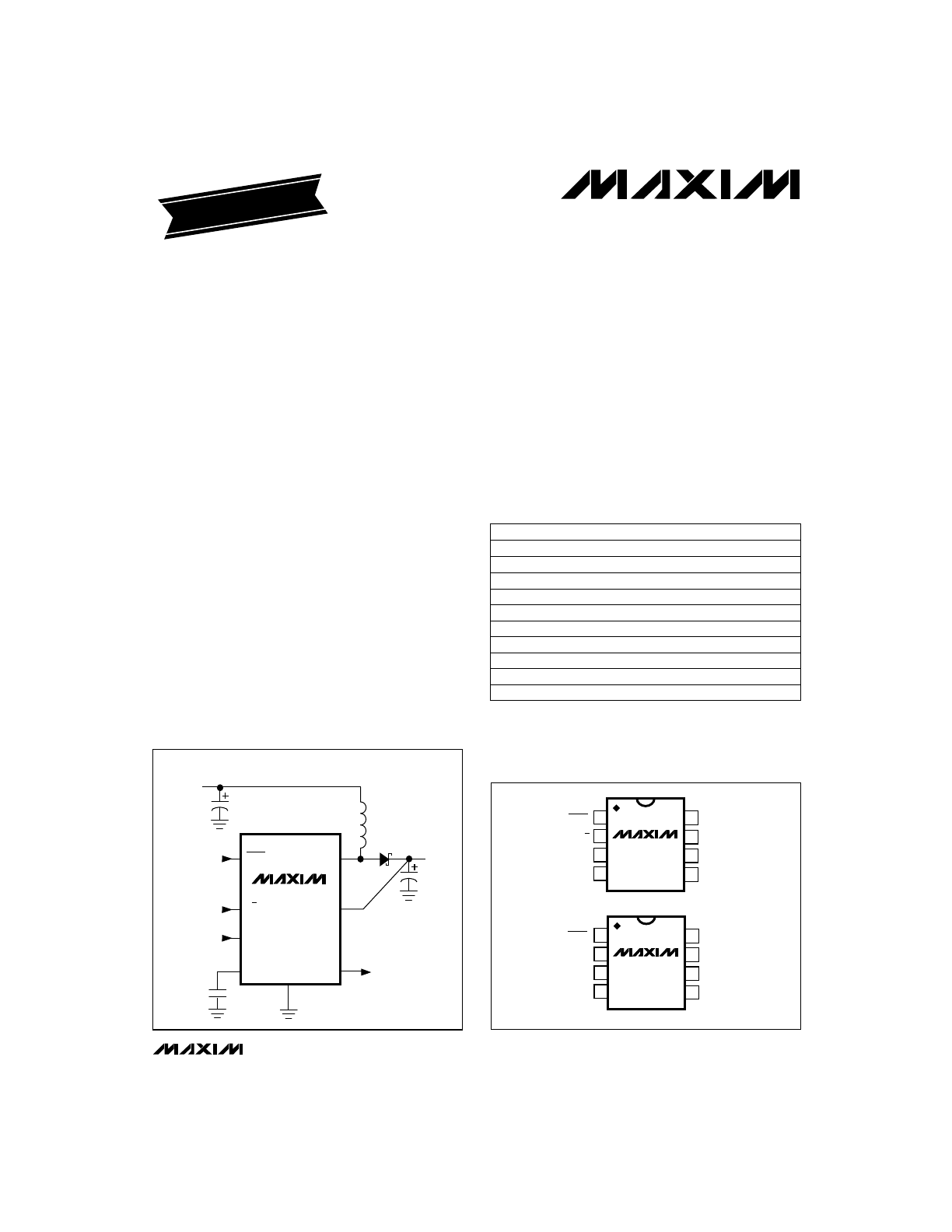
__________________Pin Configuration
MAX856
SHDN
3/5
REF
LX
GND
OUT
INPUT
0.8V TO V
OUT
1N5817
OUTPUT
5V AT 100mA
OR
3.3V AT 125mA
LBO
68
µ
F
47
µ
H
LOW-BATTERY
DETECTOR OUTPUT
ON/OFF
3V/5V SELECT
LBI
LOW-BATTERY
DETECTOR
INPUT
__________Typical Operating Circuit
Call toll free 1-800-998-8800 for free samples or literature.
19-0211; Rev 3; 7/95
PART
TEMP. RANGE
PIN-PACKAGE
MAX856
CSA
0°C to +70°C
8 SO
MAX856CUA
0°C to +70°C
8 µMAX
MAX856C/D
0°C to +70°C
Dice*
MAX856ESA
-40°C to +85°C
8 SO
MAX856MJA
-55°C to +125°C
8 CERDIP
†
MAX857
CSA
0°C to +70°C
8 SO
MAX857CUA
0°C to +70°C
8 µMAX
MAX857C/D
0°C to +70°C
Dice*
MAX857ESA
-40°C to +85°C
8 SO
MAX857MJA
-55°C to +125°C
8 CERDIP
†
EVALUATION KIT MANUAL
FOLLOWS DATA SHEET
MAX856–MAX859
3.3V/5V or Adjustable-Output,
Step-Up DC-DC Converters
2
_______________________________________________________________________________________
ABSOLUTE MAXIMUM RATINGS
ELECTRICAL CHARACTERISTICS
(Circuits of Figure 2, V
IN
= 2.5V, I
LOAD
= 0mA, T
A
= T
MIN
to T
MAX
, unless otherwise noted. Typical values are at T
A
= +25°C.)
Stresses beyond those listed under “Absolute Maximum Ratings” may cause permanent damage to the device. These are stress ratings only, and functional
operation of the device at these or any other conditions beyond those indicated in the operational sections of the specifications is not implied. Exposure to
absolute maximum rating conditions for extended periods may affect device reliability.
Supply Voltage (OUT to GND) ...................................-0.3V, +7V
Switch Voltage (LX to GND) .......................................-0.3V, +7V
S
—
H
—
D
—
N
–
, LBO to GND ....................................................-0.3V, +7V
LBI, REF, 3/
–
5
–
, FB to GND .........................-0.3V, (V
OUT
+ 0.3V)
Reference Current (I
REF
) ..................................................2.5mA
Continuous Power Dissipation (T
A
= +70°C)
SO (derate 5.88mW/°C above +70°C) .........................471mW
µMAX (derate 4.1mW/°C above +70°C) ......................330mW
CERDIP (derate 8.00mW/°C above +70°C) .................640mW
Reverse Battery Current (T
A
≤
+45°C, Note 1) .................750mA
Operating Temperature Ranges
MAX85_C_ _ ......................................................0°C to +70°C
MAX85_E_ _ ....................................................-40°C to +85°C
MAX85_MJA .................................................-55°C to +125°C
Junction Temperature .....................................................+150°C
Storage Temperature Range ............................-65°C to +160°C
Lead Temperature (soldering, 10sec) ............................+300°C
Note 1:
Reverse battery current is measured from the
Typical Operating Circuit’s battery input terminal to GND when the battery is
connected backwards. A reverse current of 750mA will not exceed the SO or CERDIP package dissipation limits but, if left
for an extended time (more than ten minutes), may degrade performance.
LBO = 5V
I
SINK
= 2mA
With falling edge
3/
–
5
–
= 3V, -20µA
≤
REF load
≤
250µA, C
REF
= 0.22µF
No REF load
MAX858/MAX859
I
LOAD
= 0mA, 3/
–
5
–
= 3V, LBI = 1.5V, V
OUT
= 3.47V,
(FB = 1.5V, MAX857/MAX859 only)
MAX856/MAX857
S
—
H
—
D
—
N
–
= 0V, 3/
–
5
–
= 3V, LBI = 1.5V, V
OUT
= 3.47V,
(FB = 1.5V, MAX857/MAX859 only)
2V
≤
V
IN
≤
3V
I
LOAD
= 0mA
Output set for 3.3V, measured at V
IN
in Figure 2, R3 omitted.
CONDITIONS
µA
1
LBO Output Leakage Current
V
0.4
LBO Output Voltage Low
mV
25
LBI Input Hysteresis
V
1.22
1.25
1.28
LBI Input Threshold
%
0.8
2.0
Reference-Voltage Regulation
V
1.23
1.25
1.27
Reference Voltage
mA
125
500
µA
1
5
Shutdown Quiescent Current
(Note 2)
1
µA
60
No Load Battery Current
4.80
5.0
5.20
3.17
3.3
3.43
4.80
5.0
5.20
µA
25
60
Quiescent Supply Current in
3.3V Mode (Note 2)
V
0.8
Minimum Operating Voltage
4.80
5.0
5.20
3.17
3.3
3.43
V
4.80
5.0
5.20
Output Voltage
V
0.8
1.8
Minimum Start-Up
Supply Voltage
UNITS
MIN
TYP
MAX
PARAMETER
Peak Inductor Current Limit
MAX856, 3/
–
5
–
= 0V, 0mA
≤
I
LOAD
≤
100mA
MAX856, 3/
–
5
–
= 3V, 0mA
≤
I
LOAD
≤
150mA
MAX857, V
OUT
= 5V, 0mA
≤
I
LOAD
≤
100mA
MAX858, 3/
–
5
–
= 0V, 0mA
≤
I
LOAD
≤
25mA
MAX858, 3/
–
5
–
= 3V, 0mA
≤
I
LOAD
≤
35mA
MAX859, V
OUT
= 5V, 0mA
≤
I
LOAD
≤
25mA
MAX85_C
MAX85_E/M
MAX856–MAX859
3.3V/5V or Adjustable-Output,
Step-Up DC-DC Converters
_______________________________________________________________________________________
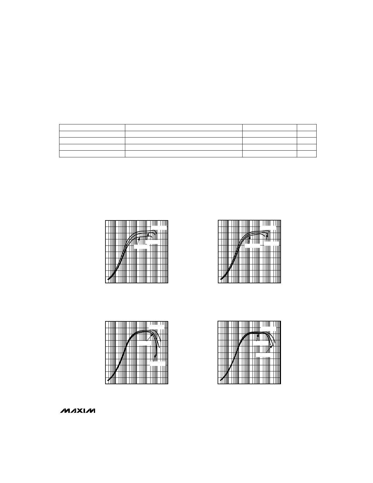
3
100
20
10
0
0.01
0.001
0.1
10
1
100
1000
MAX858/MAX859
EFFICIENCY vs. OUTPUT CURRENT
V
OUT
= 3.3V
40
30
50
MAX856-01
LOAD CURRENT (mA)
EFFICIENCY (%)
60
70
80
90
V
IN
= 2.0V
V
IN
= 2.5V
V
IN
= 1.5V
100
20
10
0
0.01
0.001
0.1
10
1
100
1000
MAX858/MAX859
EFFICIENCY vs. OUTPUT CURRENT
V
OUT
= 5V
40
30
50
MAX856-02
LOAD CURRENT (mA)
EFFICIENCY (%)
60
70
80
90
V
IN
= 2.5V
V
IN
= 3.3V
V
IN
= 1.5V
100
20
10
0
0.01
0.001
0.1
10
1
100
1000
MAX856/MAX857
EFFICIENCY vs. OUTPUT CURRENT
V
OUT
= 5V
40
30
50
MAX856-03
LOAD CURRENT (mA)
EFFICIENCY (%)
60
70
80
90
V
IN
= 2.0V
V
IN
= 3.3V
V
IN
= 1.5V
100
20
10
0
0.01
0.001
0.1
10
1
100
1000
MAX856/MAX857
EFFICIENCY vs. OUTPUT CURRENT
V
OUT
= 3.3V
40
30
50
MAX856-04
LOAD CURRENT (mA)
EFFICIENCY (%)
60
70
80
90
V
IN
= 2.0V
V
IN
= 2.5V
V
IN
= 1.5V
__________________________________________Typical Operating Characteristics
(Circuits of Figure 2, T
A
= +25°C, unless otherwise noted.)
ELECTRICAL CHARACTERISTICS (continued)
(Circuits of Figure 2, V
IN
= 2.5V, I
LOAD
= 0mA, T
A
= T
MIN
to T
MAX
, unless otherwise noted. Typical values are at T
A
= +25°C.)
Note 2:
Supply current from the 3.3V output is measured with an ammeter between the 3.3V output and OUT pin. This current
correlates directly with actual battery supply current, but is reduced in value according to the step-up ratio and efficiency.
V
OUT
= 3.47V to keep the internal switch open when measuring the current into the device.
Note 3:
Minimum value is production tested. Maximum value is guaranteed by design and is not production tested.
–
S
—
H
—
D
—
N
–
, 3/
–
5
–
Input Voltage Low
0.4
V
S
—
H
—
D
—
N
–
, 3/
–
5
–
Input Voltage High
1.6
V
S
—
H
—
D
—
N
–
, 3/
–
5
–
, FB, LBI Input Current
LBI = 1.5V, FB = 1.5V,
–
S
—
H
—
D
—
N
–
= 0V or 3V, 3/
–
5
–
= 0V or 3V
±100
nA
FB Voltage
MAX857/MAX859
1.22
1.25
1.28
V
Output Voltage Range
MAX857/MAX859, I
LOAD
= 0mA (Note 3)
2.7
6.0
V
MAX856–MAX859
3.3V/5V or Adjustable-Output,
Step-Up DC-DC Converters
4
_______________________________________________________________________________________
_____________________________Typical Operating Characteristics (continued)
(Circuits of Figure 2, T
A
= +25°C, unless otherwise noted.)
0.75
0.1
10
MAX856/MAX857
MINIMUM START-UP INPUT VOLTAGE
vs. LOAD CURRENT
MAX856-06
LOAD CURRENT (mA)
START-UP INPUT VOLTAGE (V)
0.90
1.10
0.80
1.00
1
100
1.15
1.05
0.95
0.85
V
OUT
= 3.3V
V
OUT
= 5V
0.1
10
MAX858/MAX859
MINIMUM START-UP INPUT VOLTAGE
vs. LOAD CURRENT
MAX856-07
LOAD CURRENT (mA)
START-UP INPUT VOLTAGE (V)
0.9
1.3
1.1
1
100
1.4
1.2
1.0
0.8
V
OUT
= 5V
0.8
2.0
SHUTDOWN CURRENT
vs. INPUT VOLTAGE
0.7
MAX856-11
SHUTDOWN CURRENT (
µ
A)
0.5
1.5
0.6
2.5
3.0
0.4
0.3
0.2
0.1
0
3.5
4.0
INPUT VOLTAGE (V)
T
A
= +85°C
T
A
= +25°C
T
A
= -40°C
0.9
1.0
80
2.0
MAX858/MAX859
MAXIMUM OUTPUT CURRENT
vs. INPUT VOLTAGE
70
MAX856-12
LOAD CURRENT (mA)
50
1.5
60
2.5
3.0
40
30
20
10
0
3.5
4.0
INPUT VOLTAGE (V)
90
100
1.0
V
OUT
= 5.0V
V
OUT
= 3.3V
400
1.0
MAX856/MAX857
MAXIMUM OUTPUT CURRENT
vs. INPUT VOLTAGE
350
MAX856-13
LOAD CURRENT (mA)
250
300
2.0
1.5
2.5
200
150
100
50
0
3.0
3.5
4.0
INPUT VOLTAGE (V)
V
OUT
= 5.0V
V
OUT
= 3.3V
1.6
2.0
QUIESCENT CURRENT
vs. INPUT VOLTAGE
1.4
MAX856-10
QUIESCENT CURRENT (mA)
1.0
1.5
1.2
2.5
3.0
0.8
0.6
0.4
0.2
0
3.5
4.0
INPUT VOLTAGE (V)
SEE NOTE 2
IN THE ELECTRICAL
CHARACTERISTICS
T
A
= +85°C
T
A
= -40°C
1.6
2.0
MAX858/MAX859
NO LOAD BATTERY CURRENT
vs. INPUT VOLTAGE
1.4
MAX856-09
QUIESCENT CURRENT (mA)
1.0
1.5
1.2
2.5
3.0
0.8
0.6
0.4
0.2
0
3.5
4.0
INPUT VOLTAGE (V)
INCLUDES ALL EXTERNAL
COMPONENT LEAKAGES.
CAPACITOR LEAKAGE
DOMINATES AT T
A
= +85°C.
CAPS ARE SPRAGUE 595D
T
A
= +85°C
T
A
= +25°C
T
A
= -40°C
400
2.0
MAX856/MAX857
NO LOAD BATTERY CURRENT
vs. INPUT VOLTAGE
350
MAX856-08
QUIESCENT CURRENT (
µ
A)
250
1.5
300
2.5
3.0
200
150
100
50
0
3.5
4.0
INPUT VOLTAGE (V)
T
A
= +85°C
T
A
= +25°C
T
A
= -40°C
INCLUDES ALL EXTERNAL
COMPONENT LEAKAGES.
CAPACITOR LEAKAGE
DOMINATES AT T
A
= +85°C.
CAPS ARE SPRAGUE 595 D
5
0
REFERENCE VOLTAGE vs. CURRENT
6
10
MAX856-05
REFERENCE LOAD CURRENT (
µ
A)
V
REF
LOAD REGULATION (mV)
8
7
100
200
9
50
150
250
4
3
2
1
0
MAX856–MAX859
3.3V/5V or Adjustable-Output,
Step-Up DC-DC Converters
_______________________________________________________________________________________
5
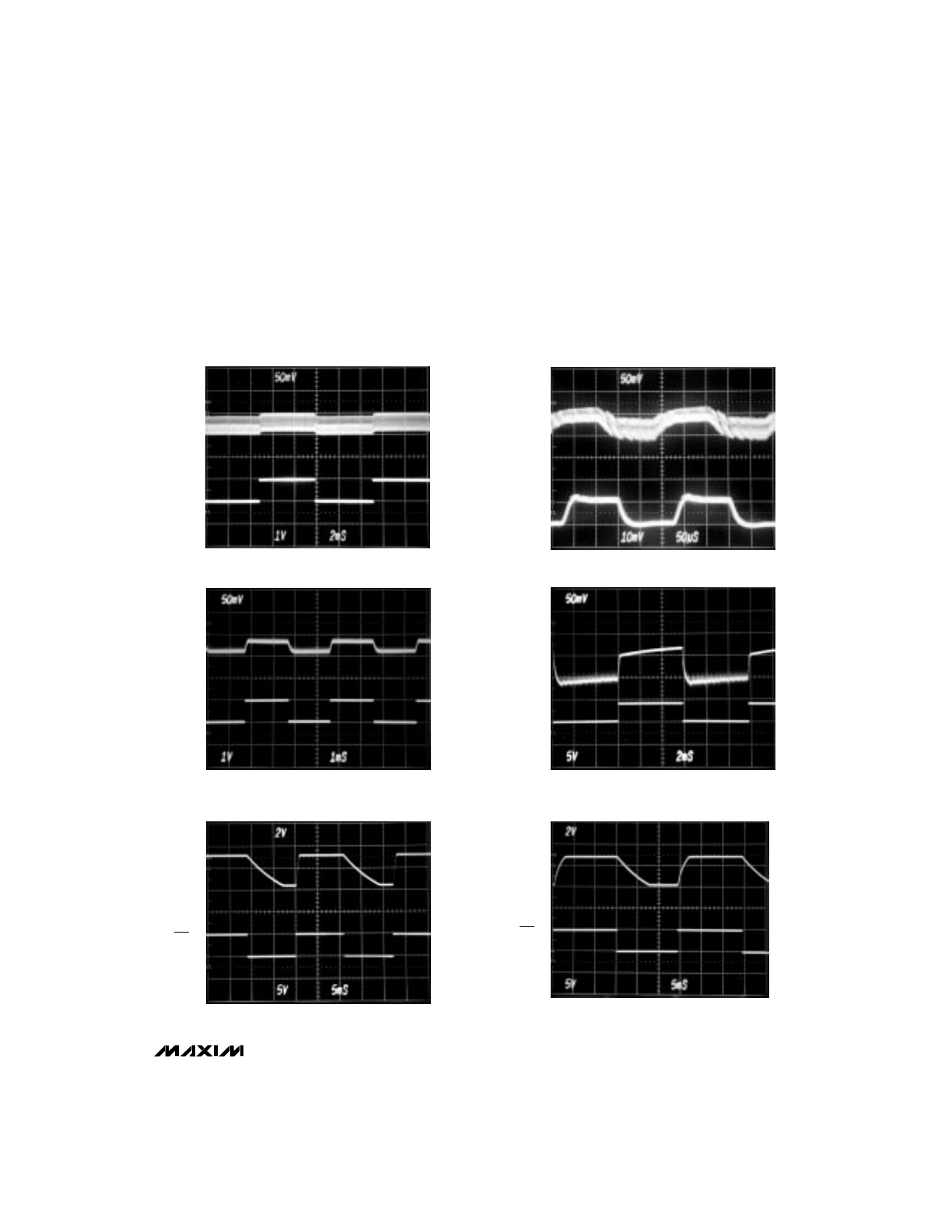
MAX856/MAX857
LINE-TRANSIENT RESPONSE (5V MODE)
2ms/div
V
OUT
50mV/div
V
IN
3V
2V
MAX856/MAX857
LOAD-TRANSIENT RESPONSE (5V MODE)
50
µ
s/div
V
OUT
50mV/div
0mA to 100mA
I
LOAD
V
IN
= 2.5V
MAX858/MAX859 LOAD-TRANSIENT RESPONSE
2ms/div
V
OUT
50mV/div
0mA to 25mA
I
LOAD
0
25
V
IN
= 2.5V
MAX859 LINE-TRANSIENT RESPONSE
1ms/div
V
OUT
50mV/div
1V/div
V
IN
3V
2V
MAX858/MAX859 START-UP DELAY (5V MODE)
5ms/div
V
OUT
2V/div
5V/div
V
SHDN
V
IN
= 2.5V, I
LOAD
= 25mA
MAX856 START-UP DELAY (5V MODE)
5ms/div
V
OUT
2V/div
5V/div
V
SHDN
V
IN
= 2.5V, I
LOAD
= 100mA
_____________________________Typical Operating Characteristics (continued)
(Circuits of Figure 2, T
A
= +25°C, unless otherwise noted.)
MAX856–MAX859
3.3V/5V or Adjustable-Output,
Step-Up DC-DC Converters
6
_______________________________________________________________________________________
______________________________________________________________Pin Description
N-Channel Power-MOSFET Drain
8
8
Low-Battery Output. An open-drain N-channel MOSFET sinks current when the voltage at
LBI drops below 1.25V.
4
4
Low-Battery Input. When the voltage on LBI drops below 1.25V, LBO sinks current.
If not used, connect to V
IN
.
5
5
Connect OUT to the regulator output. OUT provides bootstrap power to the IC.
6
6
Power Ground. Must be low impedance; solder directly to ground plane.
7
7
1.25V Reference Voltage Output. Bypass with 0.22µF to GND (0.1µF if there is no external
reference load). Maximum load capability is 250µA source, 20µA sink.
3
3
Feedback Input for adjustable-output operation. Connect to an external resistor voltage
divider between OUT and GND.
2
—
Selects the output voltage; connect to GND for 5V output, and to OUT for 3.3V
output.
—
2
Shutdown Input. When low, the entire circuit is off and V
OUT
= V
IN
- V
D,
where V
D
is the
forward voltage drop of the external Schottky rectifier.
1
1
FUNCTION
PIN
LX
LBO
LBI
OUT
GND
REF
FB
3/
–
5
–
–
S
—
H
—
D
—
N
–
NAME
MAX856
MAX858
MAX857
MAX859
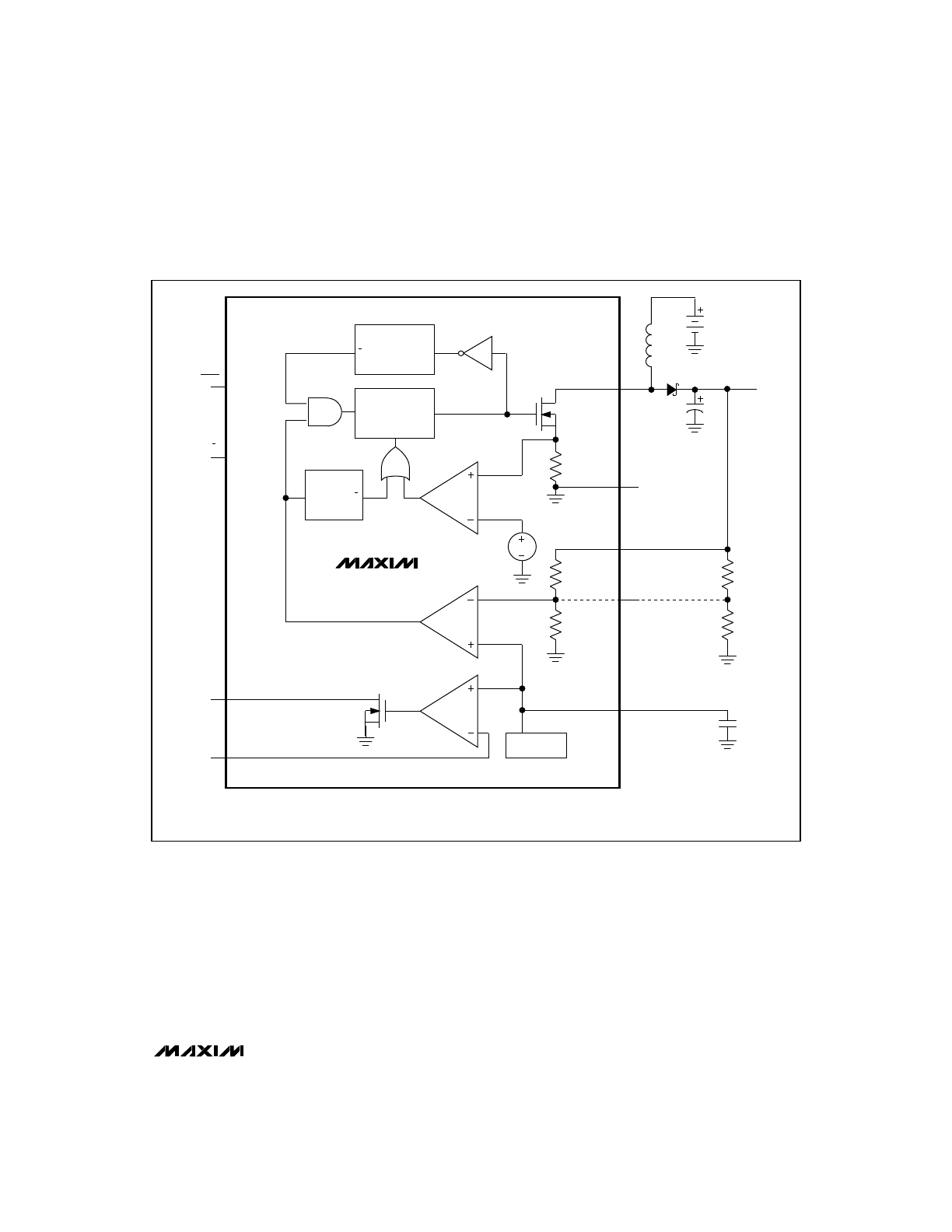
_______________Detailed Description
Operating Principle
The MAX856–MAX859 combine a switch-mode regula-
tor, N-channel power MOSFET, precision voltage refer-
ence, and power-fail detector in a single monolithic
device. The MOSFET is a “sense-FET” type for best
efficiency, and has a very low gate threshold voltage to
ensure start-up with low battery voltages (0.8V typ).
PFM Control Scheme
A unique minimum-off-time, current-limited pulse-fre-
quency modulation (PFM) control scheme is a key fea-
ture of the MAX856 series (Figure 1). This scheme
combines the high output power and efficiency of a
pulse-width modulation (PWM) device with the ultra-low
quiescent current of a traditional PFM pulse-skipper.
There is no oscillator; at heavy loads, switching is
accomplished through a constant-peak-current limit in
the switch, which allows the inductor current to vary
between this peak limit and some lesser value. At light
loads, switching frequency is governed by a pair of
one-shots, which set a minimum off-time (1µs) and a
maximum on-time (4µs). The switching frequency
depends upon the load and the input voltage, and can
range up to 500kHz.
The peak switch current of the internal MOSFET power
switch is fixed at 500mA ±100mA (MAX856/MAX857)
or 125mA ±25mA (MAX858/MAX859). The switch’s on-
resistance is typically 1
Ω
(MAX856/MAX857) or 4
Ω
(MAX858/MAX859), resulting in a switch voltage drop
(V
SW
) of about 500mV under high output loads. The
value of V
SW
will decrease with light current loads.
Conventional PWM converters generate constant-fre-
quency switching noise, whereas the unique architec-
ture of the MAX856–MAX859 produces variable-fre-
quency switching noise. However, unlike conventional
pulse-skippers (where noise amplitude varies with input
voltage), noise in the MAX856 series does not exceed
the switch current limit times the filter-capacitor equiva-
lent series resistance (ESR).
Voltage Reference
The precision voltage reference is suitable for driving
external loads, such as an analog-to-digital converter.
The voltage-reference output changes less than ±2%
when sourcing up to 250µA and sinking up to 20µA. If
the reference drives an external load, bypass it with
0.22µF to GND. If the reference is unloaded, bypass it
with at least 0.1µF.
MAX856–MAX859
3.3V/5V or Adjustable-Output,
Step-Up DC-DC Converters
_______________________________________________________________________________________
7
MAX856–MAX859
SHDN
3/5*
LBO
LBI
N
LBI COMPARATOR
ERROR COMPARATOR
CURRENT-LIMIT
COMPARATOR
ONE-SHOT
TRIG
Q
Q
ONE-SHOT
TRIG
S
Q
R
F/F
MINIMUM
OFF-TIME
ONE-SHOT
V
IN
LX
N
GND
OUT
V
OUT
**
FB**
**
*
*
REF
REFERENCE
MAXIMUM
ON-TIME
ONE-SHOT
*MAX856/MAX858 ONLY
**MAX857/MAX859 ONLY
Figure 1. Block Diagram
MAX856–MAX859
3.3V/5V or Adjustable-Output,
Step-Up DC-DC Converters
8
_______________________________________________________________________________________
Logic Inputs and Outputs
The 3/5 input is internally diode clamped
to GND
and
OUT, and should not be connected to signals outside
this range. The SHDN input and LBO output (open-
drain) are not clamped to V+ and can be pulled as high
as 7V regardless of the voltage at OUT
.
Do not leave
control inputs (3/5, LBI, or SHDN) floating.
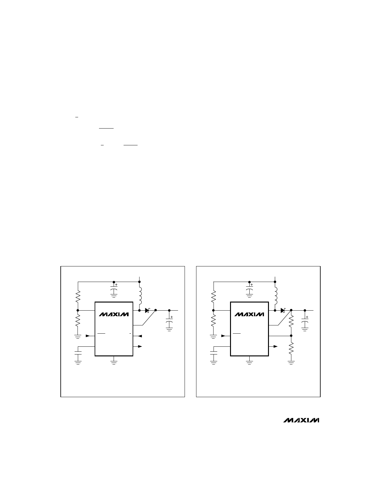
__________________Design Procedure
Output Voltage Selection
For the MAX856/MAX858,you can select a 3.3V or 5V
output voltage under logic control, or by tying 3/
–
5 to
GND or OUT. Efficiency is typically better than 80%
over a 2mA to 100mA (MAX856/MAX857) load range.
The device is internally bootstrapped, with power
derived from the output voltage (via OUT). When the
output is in 5V mode, the higher internal supply voltage
results in lower switch-transistor on-resistance, slightly
greater output power, and higher efficiency.
Bootstrapping allows the battery voltage to sag to 0.8V
once the system is started. Therefore, the battery volt-
age ranges from (V
OUT
+ V
D
) to 0.8V (where V
D
is the
forward drop of the Schottky rectifier). If the battery volt-
age exceeds the programmed output voltage, the out-
put will follow the battery voltage. This is acceptable in
many systems; however, the input or output voltage
must not be forced above 7V.
The MAX857/MAX859’s output voltage is set by two
resistors, R1 and R2 (Figure 2b), which form a voltage
divider between the output and FB. Use the following
equation to determine the output voltage:
R1 + R2
V
OUT
= V
REF
( _________ )
R2
where V
REF
= 1.25V.
To simplify resistor selection:
V
OUT
R1 = R2 ( _______ - 1)
V
REF
Since the input bias current at FB has a maximum value
of 100nA, large values (10k
Ω
to 300k
Ω
) can be used
for R1 and R2 with no significant accuracy loss. For 1%
error, the current through R1 should be at least 100
times FB’s bias current.
C1*
L1
V
IN
D1
1N5817
C2*
R1
R2
LX
OUT
FB
LBO
LBI
REF
SHDN
GND
R3
R4
C3
0.1
µ
F
V
OUT
5
1
3
8
6
2
4
7
MAX857/MAX859
*C1 = C2 = 68
µ
F FOR MAX857
47
µ
H
C1 = C2 = 22
µ
F FOR MAX859
C1*
L1
V
IN
D1
1N5817
C2*
R1
LX
OUT
3/5
LBO
LBI
REF
SHDN
GND
R3
R4
C3
0.1
µ
F
V
OUT
5
1
3
8
6
2
4
7
MAX856/MAX858
*C1 = C2 = 68
µ
F FOR MAX856
OUTPUT
SELECT
47
µ
H
C1 = C2 = 22
µ
F FOR MAX858
Figure 2b. Standard Application Circuit—Adjustable Output
Voltage
Figure 2a. Standard Application Circuit—Preset Output
Voltage

MAX856–MAX859
3.3V/5V or Adjustable-Output,
Step-Up DC-DC Converters
_______________________________________________________________________________________
9
Low-Battery Detection
The MAX856 series contains an on-chip comparator for
low-battery detection. If the voltage at LBI falls below
the regulator’s internal reference voltage (1.25V), LBO
(an open-drain output) sinks current to GND. The low-
battery monitor’s threshold is set by two resistors, R3
and R4 (Figure 2). Set the threshold voltage using the
following equation:
VLBI
R3 = R4 ( ______ - 1)
VREF
where V
LBI
is the desired threshold of the low-battery
detector and V
REF
is the internal 1.25V reference.
Since the LBI current is less than 100nA, large resistor
values (typically 10k
Ω
to 300k
Ω
) can be used for R3
and R4 to minimize loading of the input supply.
When the voltage at LBI is below the internal threshold,
LBO sinks current to GND. Connect a pull-up resistor of
10k
Ω
or more from LBO to OUT when driving CMOS
circuits. When LBI is above the threshold, the LBO out-
put is off. If the low-battery comparator is not used,
connect LBI to V
IN
and leave LBO open.
Inductor Selection
An inductor value of 47µH performs well in most
MAX856–MAX859 applications. However, the inductance
value is not critical, and the MAX856–MAX859 will work
with inductors in the 10µH to 100µH range. Smaller
inductance values typically offer a smaller physical size
for a given series resistance, allowing the smallest
overall circuit dimensions. However, due to higher peak
inductor currents, the output voltage ripple (I
PEAK
x
output filter capacitor ESR) also tends to be higher.
Circuits using larger inductance values exhibit higher
output current capability and larger physical dimen-
sions for a given series resistance.
The inductor’s incremental saturation current rating
should be greater than the peak switch-current limit,
which is 500mA for the MAX856/MAX857, and 125mA
for the MAX858/MAX859. However, it is generally
acceptable to bias the inductor into saturation by as
much as 20%, although this will slightly reduce
efficiency.
The inductor’s DC resistance significantly affects effi-
ciency. See the Efficiency vs. Load Current for Various
Inductors graph in the
Typical Operating Characteristics.
See Tables 1 and 2 for a list of suggested inductor
suppliers.
Capacitor Selection
A 68µF, 10V, 0.85
Ω
, surface-mount tantalum (SMT)
output filter capacitor typically provides 50mV output
ripple when stepping up from 2V to 5V at 100mA
(MAX856/ MAX857). Smaller capacitors (down to 10µF
with higher ESRs) are acceptable for light loads or in
applications that can tolerate higher output ripple.
Values in the 10µF to 47µF range are recommended for
the MAX858/MAX859.
The equivalent series resistance (ESR) of both bypass
and filter capacitors affects efficiency and output rip-
ple. The output voltage ripple is the product of the peak
inductor current and the output capacitor’s ESR. Use
low-ESR capacitors for best performance, or connect
two or more filter capacitors in parallel. Low-ESR, SMT
tantalum capacitors are currently available from
Sprague (595D series) and AVX (TPS series). Sanyo
OS-CON organic-semiconductor through-hole capaci-
tors also exhibit very low ESR, and are especially useful
for operation at cold temperatures. See Table 1 for a list
of suggested capacitor suppliers.
Rectifier Diode
For optimum performance, a switching Schottky diode
(such as the 1N5817) is recommended. Refer to Table
1 for a list of component suppliers. For low output
power applications, a PN-junction switching diode
(such as the 1N4148) will also work well, although its
greater forward voltage drop will reduce efficiency.
PC Layout and Grounding
The MAX856 series’ high-frequency operation makes
PC layout important for minimizing ground bounce and
noise. Keep the IC’s GND pin and the ground leads of
C1 and C2 (Figure 1) less than 0.2in (5mm) apart. Also
keep all connections to the FB and LX pins as short as
possible. To maximize output power and efficiency and
minimize output ripple voltage, use a ground plane and
solder the IC’s GND (pin 7) directly to the ground
plane.
MAX856–MAX859
3.3V/5V or Adjustable-Output,
Step-Up DC-DC Converters
10
______________________________________________________________________________________
Table 1. Component Suppliers
COMPANY
PHONE
FAX
AVX
USA:
(207) 282-5111
(207) 283-1941
Coiltronics
USA:
(407) 241-7876
(407) 241-9339
Matsuo
USA:
(714) 969-2491
(714) 960-6492
Motorola
USA:
(408) 749-0510
(800) 521-6274
Murata-Erie
USA:
(800) 831-9172
(404) 684-1541
Nichicon
USA:
(708) 843-7500
(708) 843-2798
Renco
USA:
(619) 661-6835
(516) 586-5562
Sanyo
(619) 661-1055
Japan: 81-7-2070-6306
81-7-2070-1174
Sumida
USA:
(708) 956-0666
(708) 956-0702
Japan: 81-3-3607-5111
81-3-3607-5144
United Chemi-Con
USA:
(714) 255-9500
(714) 255-9400
USA:
(516) 586-5566
CoilCraft
USA:
(708) 639-6400
(708) 639-1469
Nihon
USA:
(805) 867-2555
(805) 867-2556
Japan: 81-3-3494-7411
81-3-3494-7414
TDK
USA:
(708) 803-6100
(708) 803-6294
Japan: 03-3278-5111
03-3278-5358
RECTIFIERS
Motorola
1N5817
Maxim
MAXC001
150µF, low-ESR
electrolytic
Nichicon
PL series
low-ESR
electrolytic
United Chemi-Con
LXF series
Renco
RL 1284-22
CoilCraft
PCH-27-223
Low-Cost
Through Hole
Sanyo
OS-CON series
low-ESR organic
semiconductor
Sumida
RCH654-220
Miniature
Through Hole
Motorola MBR 0530
Nihon EC15QS02L
Matsuo 267 series
Sprague 595D series
AVX TPS series
See Table 2
Surface Mount
CAPACITORS
INDUCTORS
PRODUCTION
METHOD
MAX856–MAX859
3.3V/5V or Adjustable-Output,
Step-Up DC-DC Converters
______________________________________________________________________________________
11
__Ordering Information (continued)
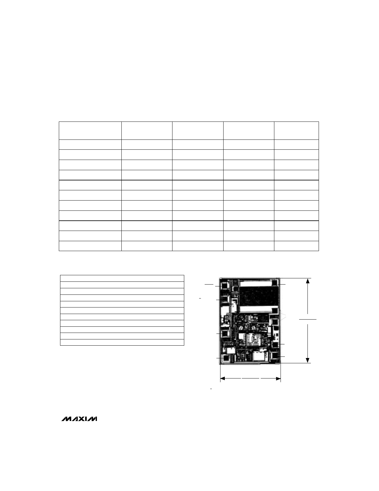
___________________Chip Topography
TRANSISTOR COUNT: 357;
SUBSTRATE CONNECTED TO OUT.
8 CERDIP
†
-55°C to +125°C
MAX859MJA
8 SO
-40°C to +85°C
MAX859ESA
Dice*
0°C to +70°C
MAX859C/D
8 µMAX
0°C to +70°C
MAX859CUA
8 SO
0°C to +70°C
MAX859
CSA
8 CERDIP
†
-55°C to +125°C
MAX858MJA
8 SO
-40°C to +85°C
MAX858ESA
Dice*
0°C to +70°C
MAX858C/D
8 µMAX
0°C to +70°C
MAX858CUA
8 SO
0°C to +70°C
MAX858
CSA
PIN-PACKAGE
TEMP. RANGE
PART
GND
LBI
OUT
3/5 OR FB*
REF
LX
0.084"
(2.1336mm)
0.058"
(1.4732mm)
SHDN
LBO
*3/5 FOR MAX856/MAX858; FB FOR MAX857/MAX859.
* Dice are tested at T
A
= +25°C only.
†
Contact factory for availability.
Table 2. Surface-Mount Inductor Information
MANUFACTURER PART
INDUCTANCE
(
m
H)
RESISTANCE
(
W
)
RATED CURRENT
(A)
HEIGHT
(mm)
Sumida CDR105B-470
47
0.14
1.0
5.0
Sumida CDR74B-470
47
0.27
0.8
4.5
Sumida CD43-470
47
0.85
0.540
3.2
Sumida CD43-220
22
0.38
0.760
3.2
Murata-Erie LQH4N220
22
0.94
0.320
2.6
Murata-Erie LQH4N470
47
1.5
0.220
2.6
Murata-Erie LQH1N220
22
3.1
0.85
1.8
TDK NLC322522T-220K
22
1.15
0.210
2.2
TDK NLC322522T-470K
47
2.25
0.150
2.2
Coiltronics CTX20-1
20
0.175
1.15
4.2
Coilcraft DT1608-223
22
0.16
0.500
3.2
MAX856–MAX859
3.3V/5V or Adjustable-Output,
Step-Up DC-DC Converters
12
______________________________________________________________________________________
________________________________________________________Package Information
DIM
A
A1
A2
A3
B
B1
C
D1
E
E1
e
eA
eB
L
MIN
–
0.015
0.125
0.055
0.016
0.045
0.008
0.005
0.300
0.240
0.100
0.300
–
0.115
MAX
0.200
–
0.175
0.080
0.022
0.065
0.012
0.080
0.325
0.310
–
–
0.400
0.150
MIN
–
0.38
3.18
1.40
0.41
1.14
0.20
0.13
7.62
6.10
2.54
7.62
–
2.92
MAX
5.08
–
4.45
2.03
0.56
1.65
0.30
2.03
8.26
7.87
–
–
10.16
3.81
INCHES
MILLIMETERS
Plastic DIP
PLASTIC
DUAL-IN-LINE
PACKAGE
(0.300 in.)
DIM
D
D
D
D
D
D
MIN
0.348
0.735
0.745
0.885
1.015
1.14
MAX
0.390
0.765
0.765
0.915
1.045
1.265
MIN
8.84
18.67
18.92
22.48
25.78
28.96
MAX
9.91
19.43
19.43
23.24
26.54
32.13
INCHES
MILLIMETERS
PINS
8
14
16
18
20
24
C
A
A2
E1
D
E
eA
eB
A3
B1
B
0° - 15°
A1
L
D1
e
L
α
C
A1
B
DIM
A
A1
B
C
D
E
e
H
L
α
MIN
0.036
0.004
0.010
0.005
0.116
0.116
0.188
0.016
0°
MAX
0.044
0.008
0.014
0.007
0.120
0.120
0.198
0.026
6°
MIN
0.91
0.10
0.25
0.13
2.95
2.95
4.78
0.41
0°
MAX
1.11
0.20
0.36
0.18
3.05
3.05
5.03
0.66
6°
INCHES
MILLIMETERS
8-PIN
µ
MAX
MICROMAX SMALL OUTLINE
PACKAGE
0.65
0.0256
A
e
E
H
D
0.101mm
0.004 in