
MAX756/MAX757
3.3V/5V/Adjustable-Output,
Step-Up DC-DC Converters
________________________________________________________________
Maxim Integrated Products
1
Call toll free 1-800-998-8800 for free samples or literature.
19-0113; Rev. 2; 1/95
_______________General Description
The MAX756/MAX757 are CMOS step-up DC-DC switch-
ing regulators for small, low input voltage or battery-pow-
ered systems. The MAX756 accepts a positive input
voltage down to 0.7V and converts it to a higher pin-
selectable output voltage of 3.3V or 5V. The MAX757 is
an adjustable version that accepts an input voltage down
to 0.7V and generates a higher adjustable output voltage
in the range from 2.7V to 5.5V. Typical full-load efficiencies
for the MAX756/MAX757 are greater than 87%.
The MAX756/MAX757 provide three improvements over
previous devices. Physical size is reduced—the high
switching frequencies (up to 0.5MHz) made possible by
MOSFET power transistors allow for tiny (<5mm diameter)
surface-mount magnetics. Efficiency is improved to 87%
(10% better than with low-voltage regulators fabricated in
bipolar technology). Supply current is reduced to 60µA
by CMOS construction and a unique constant-off-time
pulse-frequency modulation control scheme.
________________________Applications
3.3V to 5V Step-Up Conversion
Palmtop Computers
Portable Data-Collection Equipment
Personal Data Communicators/Computers
Medical Instrumentation
2-Cell & 3-Cell Battery-Operated Equipment
Glucose Meters
____________________________Features
♦
Operates Down to 0.7V Input Supply Voltage
♦
87% Efficiency at 200mA
♦
60µA Quiescent Current
♦
20µA Shutdown Mode with Active Reference and
LBI Detector
♦
500kHz Maximum Switching Frequency
♦
±1.5% Reference Tolerance Over Temperature
♦
Low-Battery Detector (LBI/LBO)
♦
8-Pin DIP and SO Packages
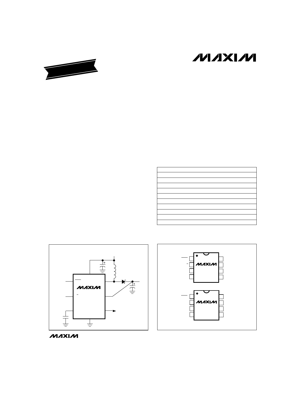
______________Ordering Information
* Dice are tested at T
A
= +25°C only.
1
2
3
4
8
7
6
5
LX
GND
OUT
LBI
LBO
REF
3/5
SHDN
MAX756
DIP/SO
TOP VIEW
1
2
3
4
8
7
6
5
LX
GND
OUT
LBI
LBO
REF
FB
SHDN
MAX757
DIP/SO
_________________Pin Configurations
MAX756
SHDN
1
3/5
2
REF
3
LBI
5
LX
7
150
µ
F
GND
OUT
6
INPUT
2V to V
OUT
1N5817
OUTPUT
5V at 200mA
or
3.3V at 300mA
100
µ
F
LBO
4
8
0.1
µ
F
22
µ
H
LOW-BATTERY
DETECTOR OUTPUT
__________Typical Operating Circuit
PART
TEMP. RANGE
PIN-PACKAGE
MAX756
CPA
0°C to +70°C
8 Plastic DIP
MAX756CSA
0°C to +70°C
8 SO
MAX756C/D
0°C to +70°C
Dice*
MAX756EPA
-40°C to +85°C
8 Plastic DIP
MAX756ESA
-40°C to +85°C
8 SO
MAX757
CPA
0°C to +70°C
8 Plastic DIP
MAX757CSA
0°C to +70°C
8 SO
MAX757C/D
0°C to +70°C
Dice*
MAX757EPA
-40°C to +85°C
8 Plastic DIP
MAX757ESA
-40°C to +85°C
8 SO
EVALUATION KIT MANUAL
FOLLOWS DATA SHEET
MAX756/MAX757
3.3V/5V/Adjustable-Output,
Step-Up DC-DC Converters
2
_______________________________________________________________________________________
Supply Voltage (OUT to GND) ....................................-0.3V, +7V
Switch Voltage (LX to GND) ........................................-0.3V, +7V
Auxiliary Pin Voltages (SHDN, LBI, LBO, REF,
3/5, FB to GND) ........................................-0.3V, (V
OUT
+ 0.3V)
Reference Current (I
REF
) ....................................................2.5mA
Continuous Power Dissipation (T
A
= +70°C)
Plastic DIP (derate 9.09mW/°C above +70°C) .............727mW
SO (derate 5.88mW/°C above +70°C) ..........................471mW
Operating Temperature Ranges:
MAX75_C_ _ ........................................................0°C to +70°C
MAX75_E_ _......................................................-40°C to +85°C
Junction Temperature ......................................................+150°C
Storage Temperature Range............................... -65°to +160°C
Lead Temperature (soldering, 10sec) ........................... +300°C
ELECTRICAL CHARACTERISTICS
(Circuits of Figure 1 and Typical Operating Circuit, V
IN
= 2.5V, I
LOAD
= 0mA, T
A
= T
MIN
to T
MAX
, unless otherwise noted.)
Stresses beyond those listed under “Absolute Maximum Ratings" may cause permanent damage to the device. These are stress ratings only, and functional
operation of the device at these or any other conditions beyond those indicated in the operational sections of the specifications is not implied. Exposure to
absolute maximum rating conditions for extended periods may affect device reliability.
ABSOLUTE MAXIMUM RATINGS
Note 1:
Supply current from the 3.3V output is measured with an ammeter between the 3.3V output and OUT pin. This current
correlates directly with actual battery supply current, but is reduced in value according to the step-up ratio and efficiency.
Note 2:
Minimum value is production tested. Maximum value is guaranteed by design and is not production tested.
LBO Output Leakage Current
SHDN, 3/5, FB, LBI Input Current
V
2.7
5.5
MAX757, I
LOAD
= 0mA (Note 2)
Output Voltage Range
V
1.22
1.25
1.28
MAX757
FB Voltage
nA
±100
LBI = 1.25V, FB = 1.25V, SHDN = 0V or 3V,
3/5 = 0V or 3V
V
1.6
SHDN, 3/5 Input Voltage High
V
0.4
SHDN, 3/5 Input Voltage Low
Shutdown Quiescent Current
(Note 1)
Battery Quiescent Current
Measured at V
IN
in Figure 1
V
1.22
1.25
1.28
With falling edge
LBI Input Threshold
mV
25
LBI Input Hysteresis
V
0.4
I
SINK
= 2mA
LBO Output Voltage Low
µA
1
LBO = 5V
µA
20
40
SHDN = 0V, LBI = 1.25V, 3/5 = 3V, V
OUT
= 3.47V,
FB = 1.3V (MAX757 only)
µA
Quiescent Supply Current in
3.3V Mode (Note 1)
MAX757, V
OUT
= 5V, 0mA < I
LOAD
< 200mA
MAX756, 3/5 = 0V, 0mA < I
LOAD
< 200mA
MAX756, 3/5 = 3V, 0mA < I
LOAD
< 300mA
%
0.8
2.0
3/5 = 3V, -20µA < REF load < 250µA, C
REF
= 0.22µF
Reference-Voltage Regulation
V
1.23
1.25
1.27
No REF load, C
REF
= 0.1µF
60
I
LOAD
= 0mA, 3/5 = 3V, LBI = 1.25V, V
OUT
= 3.47V,
FB = 1.3V (MAX757 only)
µA
V
60
Output set for 3.3V
1.1
1.8
I
LOAD
= 10mA
Minimum Start-Up Supply Voltage
4.8
5.0
5.2
2V < V
IN
< 3V
Reference Voltage
3.17
3.30
3.43
V
4.8
5.0
5.2
Output Voltage
UNITS
MIN
TYP
MAX
CONDITIONS
PARAMETER
V
0.7
I
LOAD
= 20mA
Minimum Operating Supply
Voltage (once started)
MAX756/MAX757
3.3V/5V/Adjustable-Output,
Step-Up DC-DC Converters
_________________________________________________________________________________________________
3
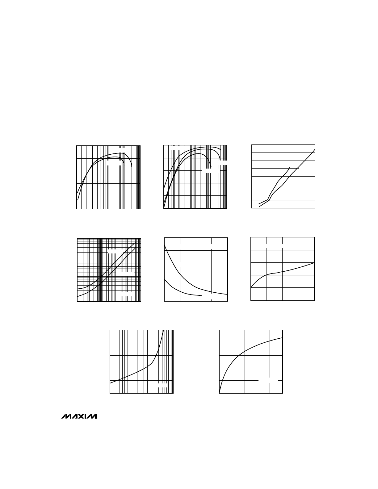
MINIMUM START-UP INPUT VOLTAGE
vs. LOAD CURRENT
MAX756-7
LOAD CURRENT (mA)
START-UP INPUT VOLTAGE (V)
10
100
1000
1
1.8
1.6
1.4
1.2
1.0
0.8
3.3V MODE
40
0.1
10
1000
EFFICIENCY vs. LOAD CURRENT
3.3V OUTPUT MODE
MAX756-1
LOAD CURRENT (mA)
EFFICIENCY (%)
60
80
90
50
70
1
100
V
IN
= 2.0V
V
IN
= 1.2V
40
0.1
10
1000
EFFICIENCY vs. LOAD CURRENT
5V OUTPUT MODE
MAX756-2
LOAD CURRENT (mA)
EFFICIENCY (%)
60
80
90
50
70
1
100
V
IN
= 3.3V
V
IN
= 2.5V
V
IN
= 1.25V
800
0
0
2
MAXIMUM OUTPUT CURRENT
vs. INPUT VOLTAGE
200
600
MAX756-3
INPUT VOLTAGE (V)
MAXIMUM OUTPUT CURRENT (mA)
4
400
100
300
500
700
1
3
5
3.3V MODE
5V MODE
1M
10
10
µ
10m
1
SWITCHING FREQUENCY
vs. LOAD CURRENT
100
MAX756-4
LOAD CURRENT (A)
SWITCHING FREQUENCY (Hz)
1k
10k
100k
100
µ
1m
100m
5V MODE
3.3V MODE
V
IN
= 2.5V
0
2
QUIESCENT CURRENT
vs. INPUT VOLTAGE
MAX756-5
INPUT VOLTAGE (V)
QUIESCENT CURRENT (
µ
A)
4
100
200
300
400
500
1
3
5
V
OUT
= 3.3V
V
OUT
= 5V
CURRENT MEASURED AT V
IN
50
0
1
2
5
SHUTDOWN QUIESCENT CURRENT
vs. INPUT VOLTAGE
20
MAX756-6
INPUT VOLTAGE (V)
SHUTDOWN QUIESCENT CURRENT (
µ
A)
4
40
10
30
3
CURRENT MEASURED AT V
IN
10
0
0
REFERENCE VOLTAGE
LOAD REGULATION
2
8
MAX756-8
LOAD CURRENT (
µ
A)
VREF LOAD REGULATION (mV)
6
4
50
100
150
200
250
V
OUT
= 3.3V
__________________________________________Typical Operating Characteristics
(Circuit of Figure 1, T
A
= +25°C, unless otherwise noted.)
MAX756/MAX757
3.3V/5V/Adjustable-Output,
Step-Up DC-DC Converters
4
_______________________________________________________________________________________
______________________________________________________________Pin Description
NAME
FUNCTION
1
SHDN
2
3/5
Selects the main output voltage setting; 5V when low, 3.3V when high.
–
FB
3
REF
4
LBO
5
LBI
6
OUT
7
GND
Power Ground. Must be low impedance; solder directly to ground plane.
8
LX
1A, 0.5
Ω
N-Channel Power MOSFET Drain
1
–
2
3
4
5
6
7
8
PIN
MAX756
MAX757
Shutdown Input disables SMPS when low, but the voltage reference and low-battery com-
parator remain active.
Feedback Input for adjustable output operation. Connect to an external voltage divider
between OUT and GND.
1.25V Reference Voltage Output. Bypass with 0.22µF to GND (0.1µF if there is no external
reference load). Maximum load capability is 250µA source, 20µA sink.
Low-Battery Output. An open-drain N-channel MOSFET sinks current when the voltage at
LBI drops below +1.25V.
Low-Battery Input. When the voltage on LBI drops below +1.25V, LBO sinks current.
Connect to V
IN
if not used.
Connect OUT to the regulator output. It provides bootstrapped power to both devices,
and also senses the output voltage for the MAX756.
OUTPUT
VOLTAGE
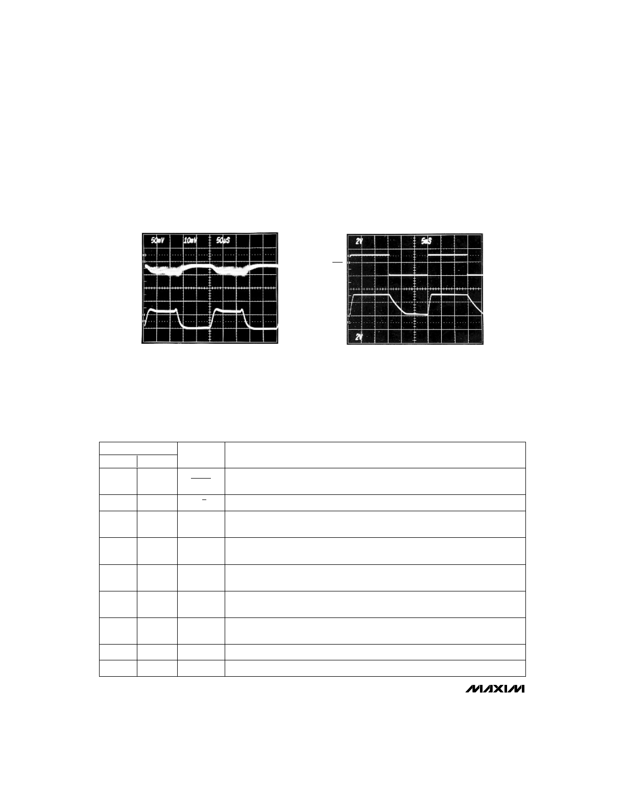
50mV/div
V
IN
= 2.5V
HORIZONTAL = 50
µ
s/div
5V Mode
LOAD-TRANSIENT RESPONSE
OUTPUT
CURRENT
0mA to 200mA
_____________________________Typical Operating Characteristics (continued)
(Circuit of Figure 1, T
A
= +25°C, unless otherwise noted.)
V
SHDN
2V/div
V
IN
= 2.5V
HORIZONTAL = 5ms/div
5V Mode
START-UP DELAY
V
OUT
2V/div
3V
0V
5V
0V

MAX756/MAX757
3.3V/5V/Adjustable-Output,
Step-Up DC-DC Converters
_______________________________________________________________________________________
5
_______________Detailed Description
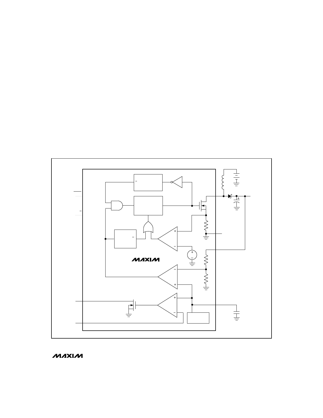
Operating Principle
The MAX756/MAX757 combine a switch-mode regulator
with an N-channel MOSFET, precision voltage reference,
and power-fail detector in a single monolithic device.
The MOSFET is a “sense-FET” type for best efficiency,
and has a very low gate threshold voltage to ensure
start-up under low-battery voltage conditions (1.1V typ).
Pulse-Frequency
Modulation Control Scheme
A unique minimum off time, current-limited, pulse-frequen-
cy modulation (PFM) control scheme is a key feature of
the MAX756/MAX757. This PFM scheme combines the
advantages of pulse-width modulation (PWM) (high output
power and efficiency) with those of a traditional PFM
pulse-skipper (ultra-low quiescent currents). There is no
oscillator; at heavy loads, switching is accomplished
through a constant peak-current limit in the switch, which
allows the inductor current to self-oscillate between this
peak limit and some lesser value. At light loads, switching
frequency is governed by a pair of one-shots, which set a
minimum off-time (1µs) and a maximum on-time (4µs).
The switching frequency depends on the load and the
input voltage, and can range as high as 500kHz.
The peak switch current of the internal MOSFET power
switch is fixed at 1A ±0.2A. The switch's on resistance
is typically 0.5
Ω
, resulting in a switch voltage drop
(V
SW
) of about 500mV under high output loads. The
value of V
SW
decreases with light current loads.
Conventional PWM converters generate constant-fre-
quency switching noise, whereas this architecture pro-
duces variable-frequency switching noise. However,
the noise does not exceed the switch current limit times
the filter-capacitor equivalent series resistance (ESR),
unlike conventional pulse-skippers.
Voltage Reference
The precision voltage reference is suitable for driving
external loads such as an analog-to-digital converter.
It has guaranteed 250µA source-current and 20µA
sink-current capability. The reference is kept alive
even in shutdown mode. If the reference drives an
external load, bypass it with 0.22µF to GND. If the ref-
erence is unloaded, bypass it with at least 0.1µF.
Control-Logic Inputs
The control inputs (3/5, SHDN) are high-impedance
MOS gates protected against ESD damage by normally
reverse-biased clamp diodes. If these inputs are dri-
ven from signal sources that exceed the main supply
voltage, the diode current should be limited by a series
resistor (1M
Ω
suggested). The logic input threshold
level is the same (approximately 1V) in both 3.3V and
5V modes. Do not leave the control inputs floating.
__________________Design Procedure
Output Voltage Selection
The MAX756 output voltage can be selected to 3.3V or
5V under logic control, or it can be left in one mode or
the other by tying 3/5 to GND or OUT. Efficiency varies
depending upon the battery and the load, and is typi-
cally better than 80% over a 2mA to 200mA load range.
The device is internally bootstrapped, with power
derived from the output voltage (via OUT). When the
output is set at 5V instead of 3.3V, the higher internal
supply voltage results in lower switch-transistor on
resistance and slightly greater output power.
Bootstrapping allows the battery voltage to sag to less
than 1V once the system is started. Therefore, the bat-
tery voltage range is from V
OUT
+ V
D
to less than 1V
(where V
D
is the forward drop of the Schottky rectifier).
If the battery voltage exceeds the programmed output
voltage, the output will follow the battery voltage. In
many systems this is acceptable; however, the output
voltage must not be forced above 7V.
The output voltage of the MAX757 is set by two resis-
tors, R1 and R2 (Figure 1), which form a voltage divider
between the output and the FB pin. The output voltage
is set by the equation:
V
OUT
= (V
REF
) [(R2 + R1) / R2]
where V
REF
= 1.25V.
To simplify resistor selection:
R1 = (R2) [(V
OUT
/ V
REF
) - 1]
Since the input bias current at FB has a maximum
value of 100nA, large values (10k
Ω
to 200k
Ω
) can be
used for R1 and R2 with no significant loss of accuracy.
For 1% error, the current through R1 should be at least
100 times FB’s bias current.
Low-Battery Detection
The MAX756/MAX757 contain on-chip circuitry for low-
battery detection. If the voltage at LBI falls below the reg-
ulator’s internal reference voltage (1.25V), LBO (an open-
drain output) sinks current to GND. The low-battery mon-
itor's threshold is set by two resistors, R3 and R4 (Figure
1), which forms a voltage divider between the input volt-
age and the LBI pin. The threshold voltage is set by R3
and R4 using the following equation:
R3 = [(V
IN
/ V
REF
) - 1] (R4)
MAX756/MAX757
3.3V/5V/Adjustable-Output,
Step-Up DC-DC Converters
6
_______________________________________________________________________________________
where V
IN
is the desired threshold of the low-battery
detector, R3 and R4 are the input divider resistors at
LBI, and V
REF
is the internal 1.25V reference.
Since the LBI current is less than 100nA, large resistor
values (typically 10k
Ω
to 200k
Ω
) can be used for R3
and R4 to minimize loading of the input supply.
When the voltage at LBI is below the internal threshold,
LBO sinks current to GND. A pull-up resistor of 10k
Ω
or more connected from LBO to V
OUT
can be used
when driving CMOS circuits. Any pull-up resistor con-
nected to LBO should not be returned to a voltage
source greater than V
OUT
. When LBI is above the
threshold, the LBO output is off. The low-battery com-
parator and reference voltage remain active when the
MAX756/MAX757 is in shutdown mode.
If the low-battery comparator is not used, connect LBI
to V
IN
and leave LBO open.
Inductor Selection
The inductors should have a saturation (incremental)
current rating equal to or greater than the peak switch-
current limit, which is 1.2A worst-case. However, it’s
generally acceptable to bias the inductor into satura-
tion by 20%, although this will reduce the efficiency.
The 22µH inductor shown in the typical applications cir-
cuit is sufficient for most MAX756/MAX757 application
circuits. Higher input voltages increase the energy
transferred with each cycle, due to the reduced
input/output differential. Minimize excess ripple due to
increased energy transfer by reducing the inductor
value (10µH suggested).
The inductor’s DC resistance significantly affects effi-
ciency. For highest efficiency, limit L1’s DC resistance
to 0.03
Ω
or less. See Table 1 for a list of suggested
inductor suppliers.
Table 1. Component Suppliers
AVX
USA:
(207) 282-5111, FAX (207) 283-1941
(800) 282-9975
CoilCraft
USA:
(708) 639-6400, FAX (708) 639-1969
Coiltronics
USA:
(407) 241-7876, FAX (407) 241-9339
Collmer
Semiconductor
USA:
(214) 233-1589
Motorola
USA:
(602) 244-3576, FAX (602) 244-4015
Nichicon
USA:
(708) 843-7500, FAX (708) 843-2798
Japan: +81-7-5231-8461, FAX (+81-) 7-5256-4158
Nihon
USA:
(805) 867-2555, FAX (805) 867-2556
Japan: +81-3-3494-7411, FAX (+81-) 3-3494-7414
Sanyo OS-CON
USA:
(619) 661-6835
Japan: +81-720-70-1005, FAX (+81-720-) 70-1174
Sprague
USA:
(603) 224-1961, FAX (603) 224-1430
Sumida
USA:
(708) 956-0666
Japan: +81-3-3607-5111, FAX (+81-3-) 3607-5428
United
Chemi-Con
USA:
(708) 696-2000, FAX (708) 640-6311
Capacitor Selection
A 100µF, 10V surface-mount (SMT) tantalum capacitor
typically provides 50mV output ripple when stepping
up from 2V to 5V at 200mA. Smaller capacitors, down
to 10µF, are acceptable for light loads or in applica-
tions that can tolerate higher output ripple.
MAX757
REF
3
LX
7
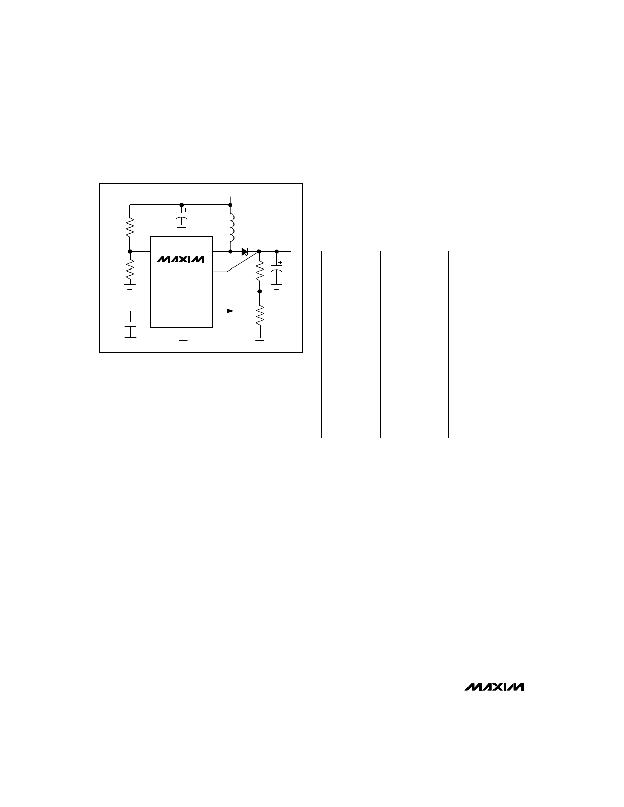
C1
150
µ
F
GND
OUT
6
V
IN
D1
1N5817
V
OUT
LBO
4
8
C3
0.1
µ
F
L1
22
µ
H
LBI
5
C2
100
µ
F
SHDN
1
FB
2
R1
R2
R3
R4
Figure 1. Standard Application Circuit
PRODUCTION
METHOD
INDUCTORS
CAPACITORS
Surface-Mount
AVX
TPS series
Sprague
595D series
Miniature
Through-Hole
Sumida
RCH654-220
Low-Cost
Through-Hole
Sumida
CD54-220 (22µH)
CoilCraft
DT3316-223
Coiltronics
CTX20-1
Sanyo OS-CON
OS-CON series
low-ESR organic
semiconductor
CoilCraft
PCH-27-223
Nichicon
PL series
low-ESR
electrolyic
United Chemi-Con
LXF series
MAX756/MAX757
3.3V/5V/Adjustable-Output,
Step-Up DC-DC Converters
_______________________________________________________________________________________
7
N
N
MAX756
GND
V
OUT
V
IN
TRIG
Q
ONE-SHOT
MINIMUM
OFF-TIME
ONE-SHOT
Q
F/F
S
R
MAXIMUM
ON-TIME
ONE-SHOT
TRIG
Q
ONE-SHOT
LX
OUT
REFERENCE
REF
LBI
LBO
3/5
SHDN
Figure 2. MAX756 Block Diagram
The ESR of both bypass and filter capacitors affects
efficiency. Best performance is obtained by using spe-
cialized low-ESR capacitors, or connecting two or more
filter capacitors in parallel. The smallest low-ESR SMT
tantalum capacitors currently available are Sprague
595D series, which are about half the size of competing
products. Sanyo OS-CON organic semiconductor
through-hole capacitors also exhibit very low ESR, and
are especially useful for operation at cold tempera-
tures. Table 1 lists suggested capacitor suppliers.
Rectifier Diode
For optimum performance, a switching Schottky diode,
such as the 1N5817, is recommended. 1N5817 equiv-
alent diodes are also available in surface-mount pack-
ages from Collmer Semiconductor in Dallas, TX, phone
(214) 233-1589. The part numbers are SE014 or
SE024. For low output power applications, a pn junc-
tion switching diode, such as the 1N4148, will also
work well, although efficiency will suffer due to the
greater forward voltage drop of the pn junction diode.
MAX756/MAX757
3.3V/5V/Adjustable-Output
Step-Up DC-DC Converters
3.3V/5V/Adjustable-Output,
Step-Up DC-DC Converters
GND
GND
LBI
OUT
3/5 (MAX756)
FB (MAX757)
REF
SHDN
LX
LBO
0.122"
(3.10mm)
0.080"
(2.03mm)
___________________Chip Topography
________________________________________________________Package Information
L
DIM
A
A1
B
C
D
E
e
H
h
L
α
MIN
0.053
0.004
0.014
0.007
0.189
0.150
0.228
0.010
0.016
0˚
MAX
0.069
0.010
0.019
0.010
0.197
0.157
0.244
0.020
0.050
8˚
MIN
1.35
0.10
0.35
0.19
4.80
3.80
5.80
0.25
0.40
0˚
MAX
1.75
0.25
0.49
0.25
5.00
4.00
6.20
0.50
1.27
8˚
INCHES
MILLIMETERS
α
8-PIN PLASTIC
SMALL-OUTLINE
PACKAGE
H
E
D
e
A
A1
C
h x 45˚
0.127mm
0.004in.
B
1.27 BSC
0.050 BSC
21-325A
PC Layout and Grounding
The MAX756/MAX757 high peak currents and high-fre-
quency operation make PC layout important for mini-
mizing ground bounce and noise. The distance
between the MAX756/MAX757’s GND pin and the
ground leads of C1 and C2 in Figure 1 must be kept to
less than 0.2" (5mm). All connections to the FB and LX
pins should also be kept as short as possible. To
obtain maximum output power and efficiency and mini-
mum output ripple voltage, use a ground plane and
solder the MAX756/MAX757 GND (pin 7) directly to the
ground plane.
TRANSISTOR COUNT: 758
SUBSTRATE CONNECTED TO OUT
8
_______________________________________________________________________________________