
_______________General Description
The MAX548A/MAX549A/MAX550A serial, 8-bit voltage-
output digital-to-analog converters (DACs) operate from
a single +2.5V to +5.5V supply. Their ±1LSB TUE spec-
ification is guaranteed over temperature. Operating cur-
rent (supply current plus reference current) is typically
75µA per DAC with V
DD
= 2.5V. In shutdown, the DAC
is disconnected from the reference, reducing current
drain to less than 1µA. The MAX548A/MAX549A allow
each DAC to be shut down independently.
The 10MHz, 3-wire serial interface is compatible with
SPI™/QSPI™ and Microwire™ interface standards.
Double-buffered inputs provide flexibility when updat-
ing the DACs; the input and DAC registers can be
updated individually or simultaneously.
The MAX548A is a dual DAC with an asynchronous
load input; it uses V
DD
as the reference input. The
MAX549A is a dual DAC with an external reference
input. The MAX550A is a single DAC with an external
reference input and an asynchronous load input.
The MAX548A/MAX549A/MAX550A’s low power con-
sumption and small µMAX and DIP packages make
these devices ideal for portable and battery-powered
applications.
________________________Applications
Battery-Powered Systems
VCXO Control
Comparator-Level Settings
GaAs Amp Bias Control
Digital Gain and Offset Control
____________________________Features
♦
+2.5V to +5.5V Single-Supply Operation
♦
±1LSB (max) TUE
♦
Power-On Reset Clears All Registers to Zero
♦
Low Operating Current:
150µA (MAX548A/MAX549A, V
REF
= +2.5V)
75µA (MAX550A, V
REF
= +2.5V)
♦
1µA Shutdown Mode
♦
10MHz, 3-Wire Serial Interface Compatible with
SPI/QSPI and Microwire
♦
µMAX Package—50% Smaller than 8-Pin SO
♦
Independent Shutdown of DACs
(MAX548A/MAX549A)
MAX548A/MAX549A/MAX550A
+2.5V to +5.5V, Low-Power, Single/Dual,
8-Bit Voltage-Output DACs in µMAX Package
________________________________________________________________
Maxim Integrated Products
1
LDAC
SCLK
DIN
1
2
8
7
V
DD
OUTB
OUTA
CS
GND
DIP/
µ
MAX
TOP VIEW
3
4
6
5
MAX548A
_________________Pin Configurations
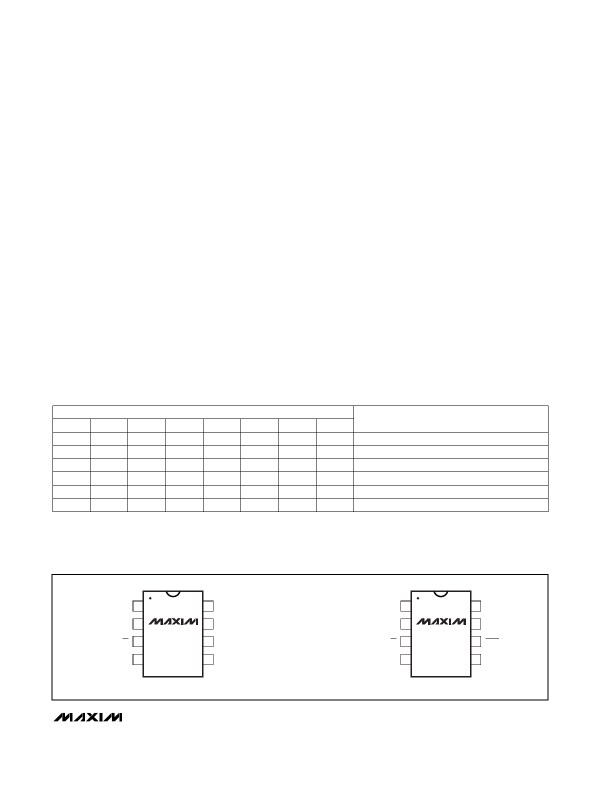
_____________________Selector Guide
19-1206; Rev 0; 3/97
PART
MAX548A
CPA
MAX548ACUA
MAX548AC/D
0°C to +70°C
0°C to +70°C
0°C to +70°C
TEMP. RANGE
PIN-PACKAGE
†
8 Plastic DIP
8 µMAX
Dice*
______________Ordering Information
Ordering Information continued at end of data sheet.
*
Dice are specified at T
A
= +25°C, DC parameters only.
†
Contact factory for availability of 8-pin SO package.
For free samples & the latest literature: http://www.maxim-ic.com, or phone 1-800-998-8800
MAX548A
MAX549A
Number of DACs
2
2
DAC Reference
V
DD
External
FEATURE
External
Asynchronous
Load DAC Input
√
MAX550A
1
—
µMAX Package
√
√
√
√
SPI and QSPI are trademarks of Motorola Inc.
Microwire is a trademark of National Semiconductor Corp.
MAX548AEPA
MAX548AEUA
-40°C to +85°C
-40°C to +85°C
8 Plastic DIP
8 µMAX
Pin Configurations continued at end of data sheet.
MAX548A/MAX549A/MAX550A
+2.5V to +5.5V, Low-Power, Single/Dual,
8-Bit Voltage-Output DACs in µMAX Package
2
_______________________________________________________________________________________
ABSOLUTE MAXIMUM RATINGS
ELECTRICAL CHARACTERISTICS
(V
DD
= +2.5V to +5.5V, T
A
= T
MIN
to T
MAX
, unless otherwise noted. Typical values are at T
A
= +25°C.)
Stresses beyond those listed under “Absolute Maximum Ratings” may cause permanent damage to the device. These are stress ratings only, and functional
operation of the device at these or any other conditions beyond those indicated in the operational sections of the specifications is not implied. Exposure to
absolute maximum rating conditions for extended periods may affect device reliability.
V
DD
, SCLK, DIN,
CS, LDAC, OUT_ to GND ...............-0.3V to 6V
REF to GND ................................................-0.3V to (V
DD
+ 0.3V)
Maximum Current (any pin) .............................................±50mA
Continuous Power Dissipation (T
A
= +70°C)
Plastic DIP (derate 9.09mW/°C above +70°C) .............727mW
µMAX (derate 4.10mW/°C above +70°C) .....................330mW
Operating Temperature Ranges
MAX5_ _AC_ A.....................................................0°C to +70°C
MAX5_ _AE_ A ..................................................-40°C to +85°C
Storage Temperature Range .............................-65°C to +150°C
Lead Temperature (soldering, 10sec) .............................+300°C
MAX549A
MAX549A/MAX550A for specified
performance
Guaranteed
monotonic
CONDITIONS
16.7
V
2.5
V
DD
V
REF
Reference Input
Voltage Range
±0.9
Bits
8
N
Resolution
LSB
±0.9
DNL
Differential Nonlinearity
LSB
±1
ZCE
Zero-Code Error
LSB
±1
FSE
Full-Scale Error
UNITS
MIN
TYP
MAX
SYMBOL
PARAMETER
MAX5_ _AEUA (Note 1)
All others
MAX549A/MAX550A
MAX548A
MAX550A
k
Ω
33.3
R
OUT
DAC Output Resistance
V
0
V
REF
DAC Output Voltage Swing
0
V
DD
k
Ω
33.3
R
REF
Reference Input Resistance
DAC Code = 55 Hex (Note 2)
MAX548A/MAX549A
%
±0.2
∆
R
OUT
/
R
OUT
DAC Output Resistance
Matching
±1
MAX5_ _AEUA (Note 1)
All others
LSB
±1
TUE
Total Unadjusted Error
MAX549A
330
550
150
250
MAX550A
165
275
µA
75
125
I
REF
Reference Input Current
DAC Code = 55 Hex (Note 3)
V
DD
= V
REF
= 5.5V
V
DD
= V
REF
= 2.5V
V
DD
= V
REF
= 5.5V
V
DD
= V
REF
= 2.5V
V
0.7V
DD
V
IH
Input High Voltage
V
0.3V
DD
V
IL
Input Low Voltage
V
IN
= 0V or V
DD
µA
±1
I
IN
Input Current
pF
10
C
IN
Input Capacitance (Note 4)
STATIC PERFORMANCE
REFERENCE INPUT
DAC OUTPUT
DIGITAL INPUTS
MAX548A/MAX549A/MAX550A
+2.5V to +5.5V, Low-Power, Single/Dual,
8-Bit Voltage-Output DACs in µMAX Package
_______________________________________________________________________________________
3
ELECTRICAL CHARACTERISTICS (continued)
(V
DD
= +2.5V to +5.5V, T
A
= T
MIN
to T
MAX
, unless otherwise noted. Typical values are at T
A
= +25°C)
TIMING CHARACTERISTICS
(V
DD
= +2.5V to +5.5V, T
A
= T
MIN
to T
MAX
, unless otherwise noted. Digital inputs switching from 0V to V
DD
.) (Figure 3) (Note 4)
Note 1:
Cold temperature specifications (to -40°C) guaranteed by design using six sigma design limits.
Note 2:
Worst-case input resistance at REF occurs at DAC code 55 hex.
Note 3:
Worst-case reference input current occurs at DAC code 55 hex.
Note 4:
Guaranteed by design. Not production tested.
Note 5:
I
DD
measured with DACs loaded with worst-case DAC code 55 hex.
CS = high, all digital inputs from 0V to V
DD
C
L
= 20pF
To ±1/2LSB, C
L
= 20pF
V/µs
3.1
µs
1.4
Voltage-Output Settling Time
4
CONDITIONS
50
nV-sec
Digital Feedthrough and
Crosstalk
UNITS
MIN
TYP
MAX
SYMBOL
PARAMETER
Voltage-Output Slew Rate
C
L
= 20pF
µs
Wake-Up Time at Power-Up
4
V
DD
= 2.5V
V
DD
= 5.5V
Supply Voltage Range
Outputs unloaded, all inputs = GND or V
DD
V
DD
V
2.5
5.5
Supply Current
(MAX549A/MAX550A)
Outputs unloaded,
all inputs = GND or
V
DD
(Note 5)
µA
330
550
I
DD
Supply Current (MAX548A)
Outputs unloaded, all inputs = GND or V
DD
;
V
DD
= 5.5V
I
DD
µA
0.3
10
V
DD
= 5.5V
V
DD
= 2.5V
Shutdown Current
Shutdown mode
µA
0.3
150
250
80
50
SCLK Period
t
CP
CS High to LDAC Low
ns
t
CSLD
ns
MAX548A/MAX550A only
5
V
DD
High to CS Low
µs
50
LDAC Pulse Width Low
t
LDAC
ns
MAX548A/MAX550A only
40
CS Pulse Width High
t
CSW
ns
20
t
CSH1
ns
V
DD
= 5.5V
10
30
t
DH
CS High to SCLK High Setup
ns
t
CSS1
ns
10
Delay, SCLK High to CS High
V
DD
= 2.5V
V
DD
= 5.5V
30
CS Low to SCLK High Setup
t
CSS0
ns
30
DIN to SCLK High Setup
t
DS
ns
0
DIN to SCLK High Hold
V
DD
= 2.5V
40
SCLK Pulse Width Low
t
CL
ns
PARAMETER
SYMBOL
MIN
TYP
MAX
UNITS
CONDITIONS
40
SCLK Pulse Width High
t
CH
ns
DYNAMIC PERFORMANCE
POWER SUPPLIES
10
SCLK High to CS Low Hold
t
CSH0
ns
MAX548A/MAX549A/MAX550A
+2.5V to +5.5V, Low-Power, Single/Dual,
8-Bit Voltage-Output DACs in µMAX Package
4
_______________________________________________________________________________________
__________________________________________Typical Operating Characteristics
(V
DD
= V
REF
= 2.5V, R
L
= 1M
Ω
, C
L
= 15pF, T
A
= +25°C, unless otherwise noted.)
-60
-20
20
100
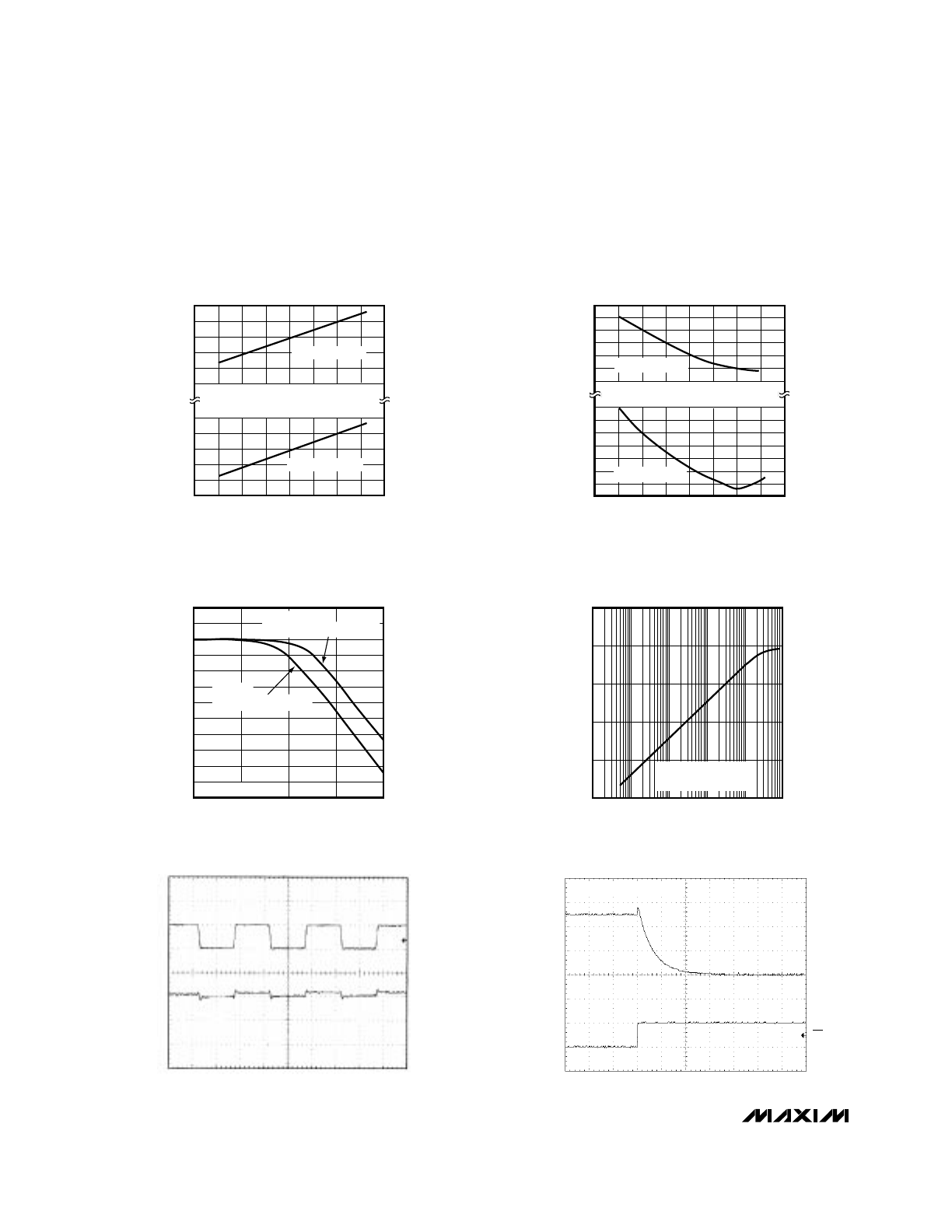
OPERATING CURRENT PER DAC
vs. TEMPERATURE
75.0
74.6
149.8
150.2
MAX548A-550A TOC-01
TEMPERATURE (°C)
OPERATING CURRENT PER DAC (
µ
A)
60
149.4
75.4
V
DD
= V
REF
= 5.0V
V
DD
= V
REF
= 2.5V
-60
-20
20
100
SHUTDOWN CURRENT
vs. TEMPERATURE
36
32
28
160
200
240
MAX548A-550A TOC-02
TEMPERATURE (°C)
SHUTDOWN CURRENT (nA)
60
120
40
V
DD
= V
REF
= 5.0V
V
DD
= V
REF
= 2.5V
-50
1k
10k
100k
1M
10M
MAX549A/MAX550A
REFERENCE SMALL-SIGNAL
FREQUENCY RESPONSE
-40
10
0
MAX548A-550A TOC-03
FREQUENCY (Hz)
RELATIVE OUTPUT (dB)
-20
-30
-10
DAC CODE = FF hex
V
DD
= 5V
V
REF
= 2Vp-p SINE WAVE
V
DD
= 2.5V
V
REF
= 100mVp-p SINE WAVE
0
-100
10
1M
100k
10k
1k
100
MAX549A/MAX550A
REFERENCE AC FEEDTHROUGH
vs. FREQUENCY
-60
-80
MAX548A-550A TOC-04
FREQUENCY (Hz)
RELATIVE OUTPUT (dB)
-40
-20
V
REF
= 1Vp-p SINE WAVE
DAC CODE = 00 hex
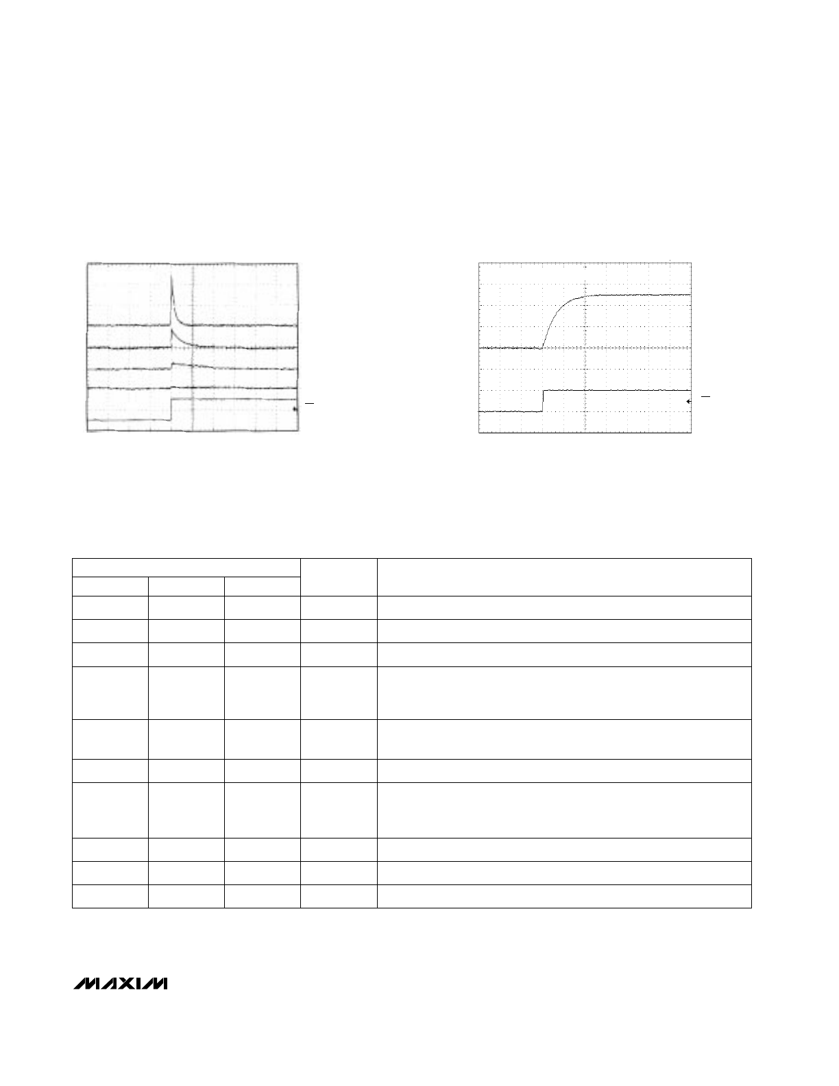
DIGITAL FEEDTHROUGH
SCLK, 5V/div
OUT, 50mV/div
200ns/div
MAX548A-550A TOC-05
SETTLING TIME (FALLING)
OUT, 1V/div
2
µ
s/div
MAX548A-550A TOC-06
CS, 5V/div
DAC CODE FF hex to 00 hex
MAX548A/MAX549A/MAX550A
+2.5V to +5.5V, Low-Power, Single/Dual,
8-Bit Voltage-Output DACs in µMAX Package
_______________________________________________________________________________________
5
OUTPUT GLITCH FILTERING
OUT, 50mV/div, C
L
= 0pF
OUT, 50mV/div, C
L
= 100pF
OUT, 50mV/div, C
L
= 220pF
5
µ
s/div
OUT, 50mV/div, C
L
= 1000pF
MAX548A-550A TOC-07
CS, 5V/div
CODE = 00 hex
_____________________________Typical Operating Characteristics (continued)
(V
DD
= V
REF
= 2.5V, R
L
= 1M
Ω
, C
L
= 15pF, T
A
= +25°C, unless otherwise noted.)
SETTLING TIME (RISING)
OUT, 1V/div
2
µ
s/div
MAX548A-550A TOC-08
CS, 5V/div
DAC CODE 00 hex to FF hex
______________________________________________________________Pin Description
Ground
1
1
1
GND
DAC A Output Voltage
2
2
—
OUTA
Chip-Select Input. A logic low on CS enables serial data to be
clocked into the input shift register. Programming commands are
executed at CS’s rising edge.
3
3
3
CS
DAC Output Voltage
—
—
2
OUT
Serial-Clock Input. Data is clocked in on SCLK’s rising edge.
5
5
5
SCLK
DAC B Output Voltage
6
7
—
OUTB
Load DAC Input. After CS goes high and if programmed by the
control word, a falling edge on LDAC updates the DAC latch(es).
Connect LDAC to V
DD
if unused.
—
6
6
LDAC
Serial-Data Input. Data is clocked into the 16-bit input shift register on
SCLK’s rising edge.
4
4
4
DIN
Positive Power Supply (+2.5V to +5.5V)
8
8
8
V
DD
External Reference Voltage Input for DAC(s)
7
—
7
REF
MAX548A
MAX549A
MAX550A
NAME
FUNCTION
PIN
MAX548A/MAX549A/MAX550A
+2.5V to +5.5V, Low-Power, Single/Dual,
8-Bit Voltage-Output DACs in µMAX Package
6
_______________________________________________________________________________________
_______________Detailed Description
Analog Section
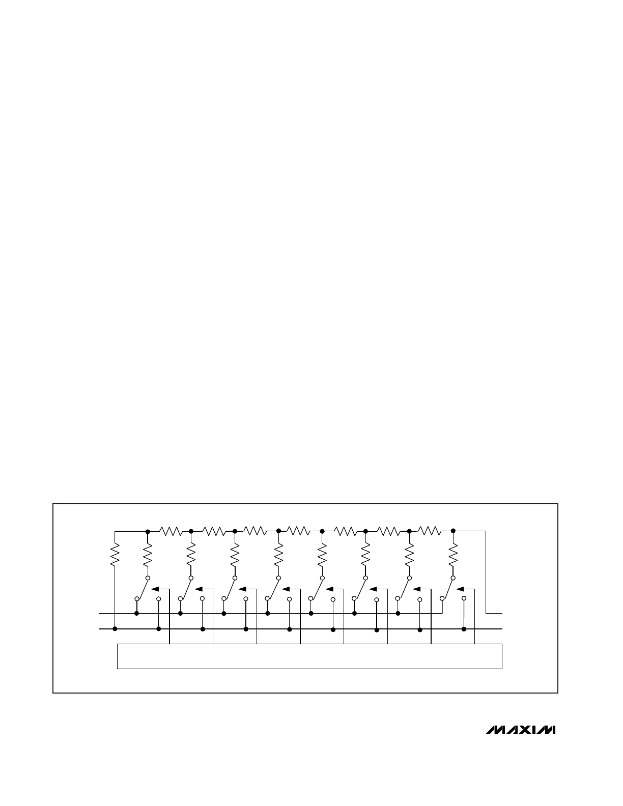
The MAX548A/MAX549A/MAX550A are 8-bit, voltage-
output digital-to-analog converters (DACs). The
MAX548A/MAX549A are dual DACs, and the MAX550A
is a single DAC. Each DAC consists of an R-2R ladder
network that converts 8-bit digital inputs into equivalent
analog output voltages in proportion to the applied ref-
erence voltage (Figure 1).
The DACs feature double-buffered inputs and
unbuffered outputs. The MAX549A/MAX550A require
an external reference. The MAX548A’s reference inputs
are internally connected to V
DD
. The power-supply
range is from +2.5V to +5.5V.
Reference Input
The voltage applied at REF (V
DD
for the MAX548A) sets
the full-scale output for all the DACs and may range
from +2.5V to V
DD
. The REF input resistance is code
dependent, with the lowest value occurring with code
01010101 (55 hex). To minimize INL errors, the refer-
ence voltage source should have less than 3
Ω
output
impedance.
DAC Output
The MAX548A/MAX549A/MAX550A contain DACs with
unbuffered outputs; each output connects directly to an
R-2R ladder. Typical output impedance is 33.3k
Ω
. This
configuration minimizes power consumption and
reduces offset errors. For highest accuracy, apply high
resistive loads (1M
Ω
and up). Lower resistive loads can
be driven, but output loading increases full-scale error.
The magnitude of the expected error is the ratio of the
DAC output resistance to the DC load resistance at the
output.
Typically, an energy pulse is coupled into the DAC out-
put on CS’s rising edge. Since each DAC output is
unbuffered, connecting a small capacitor (200pF to
1000pF) from the output to ground creates a lowpass
filter that effectively suppresses the pulse for sensitive
applications (see
Typical Operating Characteristics).
Shutdown Mode
When the MAX548A/MAX549A/MAX550A are in shut-
down mode, the R-2R ladder disconnects from the refer-
ence source. The MAX549A/MAX550A supply current
does not change, but the REF input current decreases to
less than 1µA. This allows the externally applied system
reference to remain active with minimal power
consumption. The MAX548A supply current also
decreases to less than 1µA in shutdown mode. When the
MAX548A/MAX549A/MAX550A exit shutdown mode,
recovery time is equivalent to the DAC’s settling time.
Serial Interface
The serial interface is SPI/QSPI and Microwire compati-
ble. An active-low chip select (CS) enables the input
shift register to receive data from the serial input (DIN).
Data is clocked into the shift register on the rising edge
of the serial-clock signal (SCLK). The clock frequency
can be as high as 10MHz.
Transmit data MSB first in one 16-bit word or two 8-bit
bytes. The write cycle can be segmented to allow two
8-bit-wide transfers when CS remains low. After all 16
bits are clocked into the input shift register, a rising
2R
R
R
R
R
2R
2R
2R
2R
2R
REF
GND
NOTE: SWITCH POSITIONS SHOWN FOR DAC CODE FF HEX.
DAC_ REGISTER
OUT_
MSB
LSB
GND
2R
R
R
R
2R
2R
2R
2R
Figure 1. DAC Simplified Circuit Diagram
edge on CS programs the DAC. The input registers can
be loaded independently or simultaneously without
updating the DAC registers. This allows both DAC reg-
isters to be updated simultaneously with different digital
values. The DAC outputs reflect the data stored in the
DAC registers. LDAC can be used to asynchronously
update the DAC registers independently of CS
(MAX548A/MAX550A). With C1 set high, setting C0 in
the control word forces the DAC register(s) to be
updated on LDAC’s falling edge, rather than CS’s rising
edge (Table 1).
Initialization
The MAX548A/MAX549A/MAX550A have an internal
power-on reset. At power-up, all internal registers are
reset to zero; therefore, an initialization write sequence
is not necessary.
Serial-Input Data Format and Control Codes
The control byte determines which input registers/DAC
registers are updated (Table 1). The DAC input regis-
ters are updated on the rising edge of CS. The DAC
registers can be updated on CS’s rising edge or on
LDAC’s falling edge after CS goes high. Bit C0 of the
control byte determines how the DAC registers are
updated for the MAX548A/MAX550A. The MAX549A
has no LDAC pin; the DAC registers are always up-
dated on CS’s rising edge (C0 in the control byte has
no effect).
Tables 2, 3, and 4 list the serial-input command format
for the MAX548A, MAX549A, and MAX550A, respec-
tively. The 16-bit input word consists of an 8-bit control
byte and an 8-bit data byte. The control byte is not
decoded internally. Every control bit performs one
MAX548A/MAX549A/MAX550A
+2.5V to +5.5V, Low-Power, Single/Dual,
8-Bit Voltage-Output DACs in µMAX Package
_______________________________________________________________________________________
7
UB3
X
Unassigned Bit 3
C2
1
Power-Down Mode
C2
0
Power-Up Mode
C1
1
DAC Register Load Operation Enabled
C0
1
DAC Register Updated on LDAC’s Falling Edge (MAX549A = Don’t Care)
C0
0
DAC Register Updated on CS’s Rising Edge
C1
0
DAC Register Load Operation Disabled
A1
1
Address DAC B (MAX550A = Don’t Care)
A0
1
Address DAC A
A0
UB2
0
Do Not Address DAC A
D6
—
DAC Data Bit 6
D4
X
—
DAC Data Bit 4
D5
Unassigned Bit 2
STATE
—
DAC Data Bit 5
D7
—
DAC Data Bit 7 (MSB)
A1
0
Do Not Address DAC B (MAX550A = Don’t Care)
D2
OPERATION
—
DAC Data Bit 2
D0**
DATA
BYTE
—
DAC Data Bit 0 (LSB)
D1
—
DAC Data Bit 1
D3
—
DAC Data Bit 3
Table 1. Control-Byte/Input-Word Bit Definitions
X = Don’t care *
Clocked in first
**
Clocked in last
UB1*
X
Unassigned Bit 1
CONTROL BYTE
BIT NAME
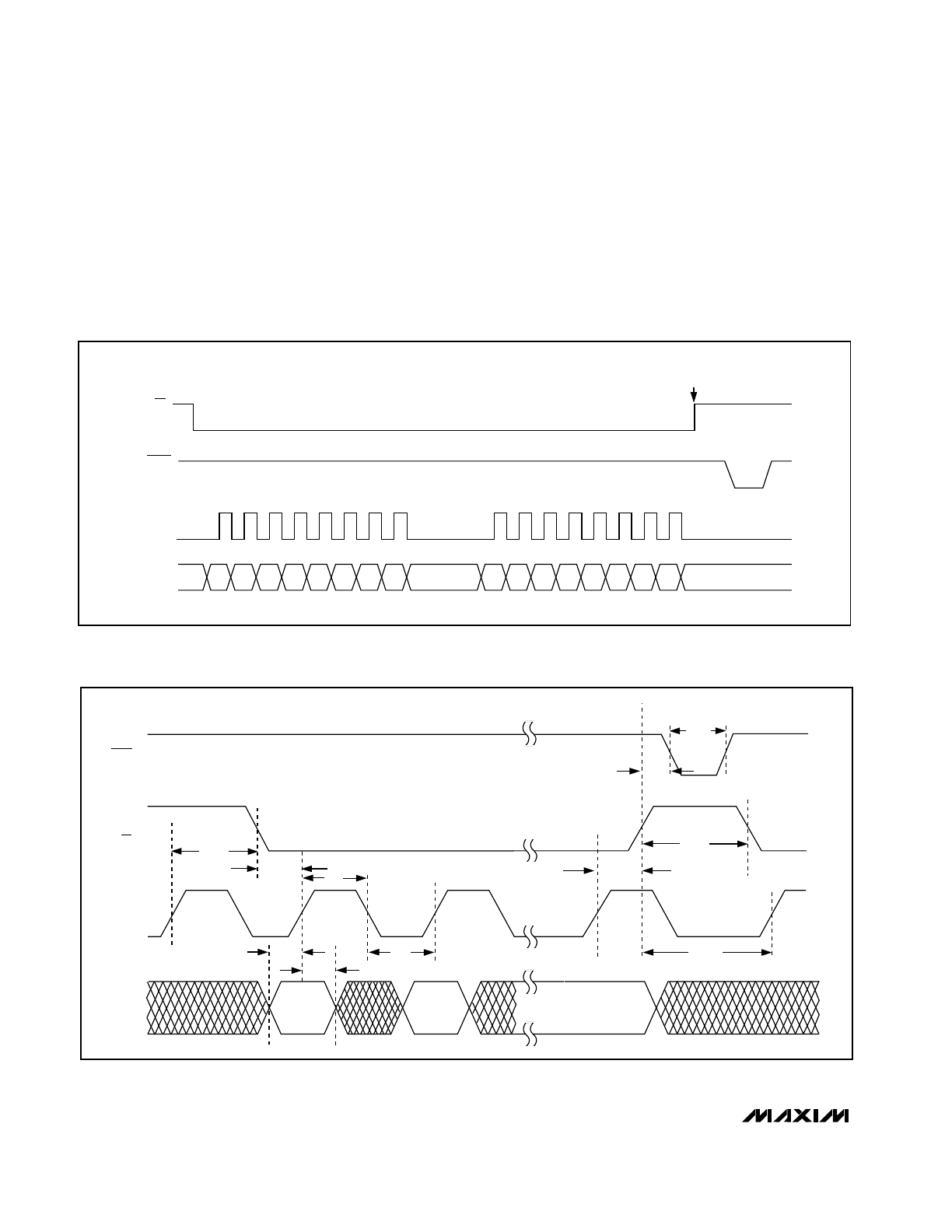
MAX548A/MAX549A/MAX550A
function. Data is clocked in starting with unassigned bit
1 (UB1), followed by the remaining control bits and the
DAC data byte. The data byte’s LSB (D0) is the last bit
clocked into the input register (Figure 2).
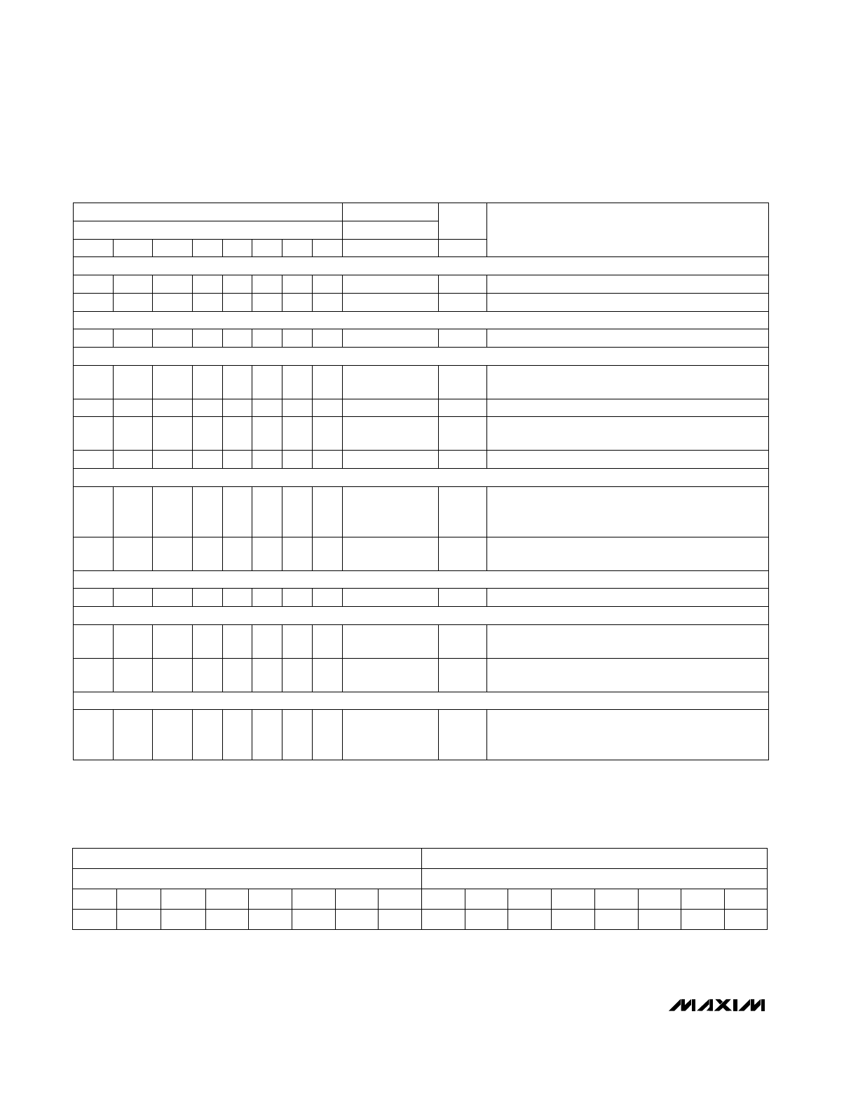
Table 5 is an example of a 16-bit input word that per-
forms the following functions:
• Loads 80 hex (128 decimal) into the DAC input regis-
ter (DAC A for the MAX548A/MAX549A)
• Updates the DAC register(s) on CS’s rising edge.
Table 6 shows how to calculate the output voltage
based on the input code. Figure 3 gives detailed timing
information.
+2.5V to +5.5V, Low-Power, Single/Dual,
8-Bit Voltage-Output DACs in µMAX Package
8
_______________________________________________________________________________________
DIN
SCLK
1
8
9
16
LDAC
MAX548A/
MAX550A
ONLY
UB1 UB2 UB3 C2
C1
C0
A1
A0
D7
D6
D5
D4
D3
D2
D1
D0
OPTIONAL
PAUSE
CS
INSTRUCTION
EXECUTED
Figure 2. Serial-Interface Timing Diagram
CS
SCLK
DIN
t
DS
t
DH
t
CL
t
CH
t
CSS0
t
CSH0
t
LDAC
t
CSW
t
CSH1
t
CSS1
t
CSLD
LDAC
Figure 3. Detailed Serial-Interface Timing Diagram
MAX548A/MAX549A/MAX550A
+2.5V to +5.5V, Low-Power, Single/Dual,
8-Bit Voltage-Output DACs in µMAX Package
_______________________________________________________________________________________
9
Table 2. MAX548A Serial-Interface Programming Commands
COMMAND
(Commands executed on
CS
’s rising edge)
LDAC
COMMANDS LOADING INPUT REGISTER(S) ONLY
X
Unassigned operation
X
XXXXXXXX
0
0
X
X
X
1
X
X
Unassigned command
X
XXXXXXXX
0
0
X
0
X
0
X
CONTROL BYTE
Loaded First
Loaded Last
UB1
Pin 6
D7........D0
A0
A1
C0
C1
UB3
C2
UB2
X
Load DAC B input register and update both DAC
registers. DAC A input register unchanged.
0
8-Bit DAC Data
X
Load DAC A input register and update both DAC
registers. DAC B input register unchanged.
0
8-Bit DAC Data
0
1
1
1
X
0
X
1
0
1
1
X
0
X
Update both DAC registers with current contents
of their input registers. Both input registers
unchanged.
0
0
0
1
1
X
0
X
X
X
Load both DAC input registers and update both
DAC registers.
X
8-Bit DAC Data
1
1
0
1
X
0
X
X
Load DAC B input register and update both DAC
registers. DAC A input register unchanged.
X
8-Bit DAC Data
0
1
0
1
X
0
X
X
Load both DAC input registers. Both DAC regis-
ters unchanged.
X
8-Bit DAC Data
1
1
X
0
X
0
X
X
Load DAC B input register. DAC A input register
and both DAC registers unchanged.
X
8-Bit DAC Data
0
1
X
0
X
0
X
X
Load DAC A input register and update both DAC
registers. DAC B input register unchanged.
X
8-Bit DAC Data
1
0
0
1
X
0
X
X
Load DAC A input register. DAC B input register
and both DAC registers unchanged.
Update both DAC registers with current contents
of their input registers. Both input registers
unchanged.
X
X
8-Bit DAC Data
XXXXXXXX
1
0
0
0
X
0
0
1
X
0
X
0
X
X
X
UNASSIGNED COMMANDS
DATA BYTE
XXXXXXXX
COMMANDS UPDATING DAC REGISTER(S)
X
Load both DAC input registers and update both
DAC registers.
0
8-Bit DAC Data
1
1
1
1
X
0
X
COMMANDS UTILIZING THE ASYNCHRONOUS LOAD FUNCTION
X
After CS’s rising edge and on LDAC’s falling
edge, update both DAC registers with current
contents of their input registers. Both input regis-
ters unchanged.
1
XXXXXXXX
0
0
1
1
X
0
X
X
Load DAC A input register. After CS’s rising edge
and on LDAC’s falling edge, update both DAC
registers.
1
8-Bit DAC Data
1
0
1
1
X
0
X
X
Load DAC B input register. After CS’s rising edge
and on LDAC’s falling edge, update both DAC
registers.
1
8-Bit DAC Data
0
1
1
1
X
0
X
X
Load both DAC input registers. After CS’s rising
edge and on LDAC’s falling edge, update both
DAC registers.
1
8-Bit DAC Data
1
1
1
1
X
0
X
MAX548A/MAX549A/MAX550A
+2.5V to +5.5V, Low-Power, Single/Dual,
8-Bit Voltage-Output DACs in µMAX Package
10
______________________________________________________________________________________
Table 2. MAX548A Serial-Interface Programming Commands (continued)
COMMANDS FOR POWERING DOWN
X
1
X
0
X
1
0
CONTROL BYTE
8-Bit DAC Data
X
Load DAC B input register and power down DAC
B. DAC A registers unchanged.
X
X
1
X
0
X
1
1
8-Bit DAC Data
X
Load both DAC input registers and power down
both DACs. Both DAC registers unchanged
X
X
1
X
1
0
1
0
8-Bit DAC Data
X
Load DAC B input register, power down DAC B,
and update both DAC registers. DAC A input
register unchanged.
X
X = Don’t care
X
1
X
1
0
0
1
8-Bit DAC Data
X
Load DAC A input register, power down DAC A,
and update both DAC registers. DAC B input
register unchanged.
X
X
1
X
0
X
0
1
8-Bit DAC Data
X
Load DAC A input register and power down DAC
A. DAC B registers unchanged.
X
X
1
X
1
0
1
1
8-Bit DAC Data
X
Load both DAC input registers, power down both
DACs, and update both DAC registers.
X
X
1
X
1
1
0
1
8-Bit DAC Data
0
Load DAC A input register, power down
DAC A, and update both DAC registers. DAC B
input register unchanged.
X
X
1
X
1
1
1
0
8-Bit DAC Data
0
Load DAC B input register, power down
DAC B, and update both DAC registers. DAC A
input register unchanged.
X
X
1
X
1
1
1
1
8-Bit DAC Data
0
Load both DAC input registers and power down
both DACs. Update both DAC registers.
X
X
1
X
1
1
0
1
8-Bit DAC Data
1
Load DAC A input register and power down DAC
A. While powered down, on LDAC’s falling edge,
update both DAC registers. DAC B input register
unchanged.
X
X
1
X
1
1
1
0
8-Bit DAC Data
1
Load DAC B input register and power down DAC
B. While powered down, on LDAC’s falling edge,
update both DAC registers. DAC A input register
unchanged.
X
X
1
X
1
1
1
1
8-Bit DAC Data
1
Load both DAC input registers and power down
both DACs. While powered down, on LDAC’s
falling edge, update both DAC registers.
X
COMMAND
(Commands executed on
CS
’s rising edge)
LDAC
DATA BYTE
Loaded Last
Loaded First
Pin 6
D7........D0
UB1
A0
A1
C0
C1
C2
UB3
UB2
COMMANDS POWERING DOWN AND LOADING INPUT REGISTER(S) ONLY
COMMANDS POWERING DOWN AND UPDATING DAC REGISTER(S)
COMMANDS POWERING DOWN AND UTILIZING THE ASYNCHRONOUS LOAD FUNCTION
MAX548A/MAX549A/MAX550A
+2.5V to +5.5V, Low-Power, Single/Dual,
8-Bit Voltage-Output DACs in µMAX Package
______________________________________________________________________________________
11
Table 3. MAX549A Serial-Interface Programming Commands
DATA BYTE
UNASSIGNED COMMAND
X
X
X
X
X
0
X
1
0
X
X
0
0
0
1
X
0
X
0
X
1
0
XXXXXXXX
8-Bit DAC Data
Loaded First
Update both DAC registers with current contents of their
input registers. Both input registers unchanged.
Load DAC A input register. DAC registers unchanged.
X
X
0
X
1
X
0
1
X
0
X
1
X
1
0
8-Bit DAC Data
Load DAC A input register and update both DAC
registers. DAC B input register unchanged.
X
1
X
0
X
X
0
1
X
1
X
0
X
1
0
8-Bit DAC Data
Load DAC A input register and power down DAC A.
DAC B input register and both DAC registers unchanged.
X
8-Bit DAC Data
Load DAC B input register and power down DAC B.
DAC A input register and both DAC registers unchanged.
X
Loaded Last
X
1
X
0
X
1
1
8-Bit DAC Data
Load both DAC input registers and power down both
DACs. Both DAC registers unchanged.
X
8-Bit DAC Data
Load DAC B input register. DAC registers unchanged.
X
X
0
X
0
X
1
1
8-Bit DAC Data
Load both DAC input registers. DAC registers
unchanged.
X
8-Bit DAC Data
Load DAC B input register and update both DAC
registers. DAC A input register unchanged.
X
X
0
X
1
X
1
1
8-Bit DAC Data
Load both DAC input registers and update both DAC
registers.
X
COMMAND
(Commands executed on
CS
’s rising edge)
CONTROL BYTE
UB2
C2
UB3
C1
C0
A1
A0
D7........D0
UB1
X
X
X
0
X
0
0
XXXXXXXX
Unassigned command
X
COMMANDS LOADING INPUT REGISTER(S) ONLY
COMMANDS UPDATING DAC REGISTER(S)
COMMANDS POWERING DOWN AND LOADING INPUT REGISTER(S) ONLY
X = Don’t care
COMMANDS POWERING DOWN AND UPDATING DAC REGISTER(S)
X
1
X
1
X
0
1
8-Bit DAC Data
Load DAC A input register, power down DAC A, and
update both DAC registers. DAC B input register
unchanged.
X
X
1
X
1
X
1
0
8-Bit DAC Data
Load DAC B input register, power down DAC B, and
update both DAC registers. DAC A input register
unchanged.
X
X
1
X
1
X
1
1
8-Bit DAC Data
Load both DAC input registers, power down both DACs,
and update both DAC registers.
X
MAX548A/MAX549A/MAX550A
+2.5V to +5.5V, Low-Power, Single/Dual,
8-Bit Voltage-Output DACs in µMAX Package
12
______________________________________________________________________________________
Table 4. MAX550A Serial-Interface Programming Commands
COMMANDS LOADING DAC REGISTER
COMMANDS LOADING INPUT REGISTER ONLY
UNASSIGNED COMMANDS
Loaded Last
Loaded First
LDAC
CONTROL BYTE
COMMAND
(Commands executed on
CS
’s rising edge)
X
Update DAC register with current contents of
input register. Input register unchanged.
0
0
X
1
1
X
0
X
XXXXXXXX
X
Load DAC input register and update DAC register.
0
8-Bit DAC Data
1
X
1
1
X
0
X
XXXXXXXX
X
Load DAC input register and update DAC register.
X
8-Bit DAC Data
1
X
0
1
X
0
X
UB1
Pin 6
D7........D0
A0
A1
C0
C1
UB3
C2
UB2
X
Update DAC register with current contents of
input register. Input register unchanged.
X
0
X
0
1
X
0
X
X
Load DAC input register. DAC register unchanged.
X
8-Bit DAC Data
1
X
X
0
X
0
X
X
Unassigned operation
X
XXXXXXXX
0
X
X
X
X
X
1
X
Unassigned command
X
XXXXXXXX
0
X
X
0
X
0
X
DATA BYTE
COMMANDS UTILIZING THE ASYNCHRONOUS LOAD FUNCTION
X
After CS’s rising edge and on LDAC’s falling
edge, update DAC register with current contents
of input register. Input register unchanged.
1
XXXXXXXX
0
X
1
1
X
0
X
X
Load DAC input register. After CS’s rising edge
and on LDAC’s falling edge, update DAC register.
1
8-Bit DAC Data
1
X
1
1
X
0
X
COMMAND POWERING DOWN AND LOADING INPUT REGISTER ONLY
X
Load DAC input register and power down DAC.
X
8-Bit DAC Data
1
X
X
0
X
1
X
COMMANDS POWERING DOWN AND UPDATING DAC REGISTER
X
Load DAC input register, power down DAC, and
update DAC register.
X
8-Bit DAC Data
1
X
0
1
X
1
X
X
Load DAC input register, power down DAC, and
update DAC register.
0
8-Bit DAC Data
1
X
1
1
X
1
X
COMMAND POWERING DOWN AND UTILIZING THE ASYNCHRONOUS LOAD FUNCTION
X
Load DAC input register and power down DAC.
While powered down, on LDAC’s falling edge,
update DAC register.
1
8-Bit DAC Data
1
X
1
1
X
1
X
Table 5. Example Input Word
X = Don’t care
X = Don’t care
UB2
X
C2
0
UB3
X
C0
0
CONTROL BYTE
A0
1
Loaded First
A1
0
C1
1
D6
0
D4
0
D5
0
D2
0
DATA BYTE
D0
0
Loaded Last
D1
0
D3
0
D7
1
UB1
X
MAX548A/MAX549A/MAX550A
+2.5V to +5.5V, Low-Power, Single/Dual,
8-Bit Voltage-Output DACs in µMAX Package
______________________________________________________________________________________
13
Table 6. Analog Output vs. Code
Microprocessor Interfacing
The MAX548A/MAX549A/MAX550A serial interface is
SPI/QSPI and Microwire compatible. For SPI/QSPI, clear
the CPOL and CPHA bits (CPOL = 0 and CPHA = 0).
CPOL = 0 sets the clock idle state to zero, and CPHA =
0 changes data at SCLK’s falling edge. This is the
Microwire default condition. If a serial port is not avail-
able on your microprocessor, three bits of a parallel port
can be used to emulate a serial port by bit manipulation.
Operate the serial clock only when necessary, to mini-
mize digital feedthrough at the DAC registers.
__________Applications Information
Power-Supply
and Ground Considerations
Connect GND to the highest quality ground available.
Bypass V
DD
with a 0.1µF to 0.22µF capacitor to GND.
The reference input can be used without bypassing.
However, for optimum line/load-transient response and
noise performance, bypass the reference input with a
0.1µF to 4.7µF capacitor to GND.
Careful PC board layout minimizes crosstalk in DAC regis-
ters, the reference, and the digital inputs. Separate analog
traces by running ground traces between them. Make sure
that high-frequency digital lines are not routed parallel to
analog lines.
AC Considerations
Digital Feedthrough
High-speed data at any of the digital input pins can
couple through a DAC’s internal stray package capaci-
tance and cause noise (digital feedthrough) at the DAC
output, even though LDAC and/or CS are held high
(see
Typical Operating Characteristics). Test digital
feedthrough by holding LDAC and/or CS high and tog-
gling the digital inputs from all 1s to all 0s.
Analog Feedthrough
Due to internal stray capacitance, higher frequency analog
input signals at REF can couple to the output, even when
the input digital code is all 0s. This condition is shown in
the MAX549A/MAX550A Reference AC Feedthrough vs.
Frequency graph in the
Typical Operating Characteristics.
Test analog feedthrough by setting all DAC outputs to 0V
and sweeping REF.
Note:
1LSB = V
REF
x 2
-8
= V
REF
(1 / 256); ANALOG OUTPUT = +V
REF
(I / 256), where I = Integer Value of Digital Input.
_____________________________________________Pin Configurations (continued)
OUTB
SCLK
DIN
1
2
8
7
V
DD
REF
OUTA
CS
GND
DIP/
µ
MAX
TOP VIEW
3
4
6
5
MAX549A
LDAC
SCLK
DIN
1
2
8
7
V
DD
REF
OUT
CS
GND
DIP/
µ
MAX
3
4
6
5
MAX550A
ANALOG OUTPUT (V)
+V
REF
(255 / 256)
+V
REF
(129 / 256)
0
0
0
0
1
0
0
1
+V
REF
(128 / 256) = +V
REF
/ 2
+V
REF
(127 / 256)
1
1
1
1
1
1
1
0
0
0
0
0
0
0
0
D6
1
1
D4
1
+V
REF
(1 / 256)
D5
1
0
D2
1
0
DAC CONTENTS
D0
1
0
D1
1
0
D3
1
0
D7
1
0
0
0
0
0
0
0
0
1
0
0
0
MAX548A/MAX549A/MAX550A
+2.5V to +5.5V, Low-Power, Single/Dual,
8-Bit Voltage-Output DACs in µMAX Package
14
______________________________________________________________________________________
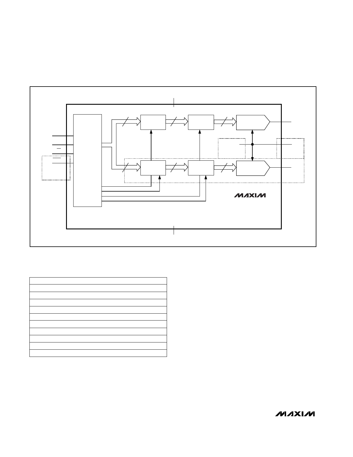
TRANSISTOR COUNT: 1562
_________________________________________________________Functional Diagram
_Ordering Information (continued)
___________________Chip Information
DAC A
INPUT
REGISTER
DAC A
REGISTER
DAC A
R-2R LADDER
SCLK
DIN
OUTA
OUTB
REF
MAX549A/
MAX550A
ONLY
V
DD
MAX548A
ONLY
MAX548A/
MAX549A
ONLY
INPUT
SHIFT
REGISTER
AND
CONTROL
8
V
DD
CS
MAX548A
MAX549A
MAX550A
GND
LDAC
MAX548A/
MAX550A
ONLY
DAC B
INPUT
REGISTER
DAC B
REGISTER
DAC B
R-2R LADDER
8
8
8
8
8
PART
MAX549A
CPA
MAX549ACUA
MAX549AC/D
0°C to +70°C
0°C to +70°C
0°C to +70°C
TEMP. RANGE
PIN-PACKAGE
8 Plastic DIP
8 µMAX
Dice*
MAX549AEPA
MAX549AEUA
-40°C to +85°C
-40°C to +85°C
8 Plastic DIP
8 µMAX
MAX550A
CPA
MAX550ACUA
MAX550AC/D
0°C to +70°C
0°C to +70°C
0°C to +70°C
8 Plastic DIP
8 µMAX
Dice*
MAX550AEPA
MAX550AEUA
-40°C to +85°C
-40°C to +85°C
8 Plastic DIP
8 µMAX
*
Dice are specified at T
A
= +25°C, DC parameters only.
MAX548A/MAX549A/MAX550A
+2.5V to +5.5V, Low-Power, Single/Dual,
8-Bit Voltage-Output DACs in µMAX Package
______________________________________________________________________________________
15
________________________________________________________Package Information
PDIPN.EPS
Maxim cannot assume responsibility for use of any circuitry other than circuitry entirely embodied in a Maxim product. No circuit patent licenses are
implied. Maxim reserves the right to change the circuitry and specifications without notice at any time.
16
__________________Maxim Integrated Products, 120 San Gabriel Drive, Sunnyvale, CA 94086 (408) 737-7600
© 1997 Maxim Integrated Products
Printed USA
is a registered trademark of Maxim Integrated Products.
MAX548A/MAX549A/MAX550A
+2.5V to +5.5V, Low-Power, Single/Dual,
8-Bit Voltage-Output DACs in µMAX Package
Maxim cannot assume responsibility for use of any circuitry other than circuitry entirely embodied in a Maxim product. No circuit patent licenses are
implied. Maxim reserves the right to change the circuitry and specifications without notice at any time.
16
__________________Maxim Integrated Products, 120 San Gabriel Drive, Sunnyvale, CA 94086 (408) 737-7600
© 1997 Maxim Integrated Products
Printed USA
is a registered trademark of Maxim Integrated Products.
___________________________________________Package Information (continued)
8LUMAXD.EPS