
_______________General Description
The MAX522 contains two 8-bit, buffered, voltage-output
digital-to-analog converters (DAC A and DAC B) in small
8-pin SO and DIP packages. DAC A’s buffer can source
and sink 5mA, and DAC B’s output can source and sink
500µA, both to within 0.5V of ground and V
DD
. The
MAX522 operates with a single +2.7V to +5.5V supply.
The device utilizes a 3-wire serial interface, which oper-
ates at clock rates up to 5MHz and is compatible with
SPI™, QSPI™, and Microwire™ interface standards.
The serial input shift register is 16 bits long and con-
sists of eight bits of DAC input data and eight bits for
DAC selection and shutdown control. DAC registers
can be loaded independently or in parallel at the posi-
tive edge of CS.
The MAX522’s ultra-low power consumption and small
8-pin SO package make it ideal for portable and bat-
tery-powered applications. Supply current is less than
1mA and drops below 1µA in shutdown mode. In addi-
tion, the reference input is disconnected from the REF
pin during shutdown, further reducing the system’s total
power consumption. The software format is compatible
with the MAX512/MAX513 triple 8-bit DACs.
________________________Applications
Digital Gain and Offset Adjustment
Programmable Current Source
Programmable Voltage Source
Power-Amp Bias Control
VCO Tuning
____________________________Features
♦
Operates from a Single +2.7V to +5.5V Supply
♦
Dual Buffered Voltage Output
♦
Low Power Consumption:
1mA Operating Current
<1µA Shutdown Current
♦
Independently Programmable Shutdown Mode
♦
5MHz, 3-Wire Serial Interface
♦
SPI™, QSPI™, and Microwire™ Compatible
♦
Space-Saving 8-Pin SO Package
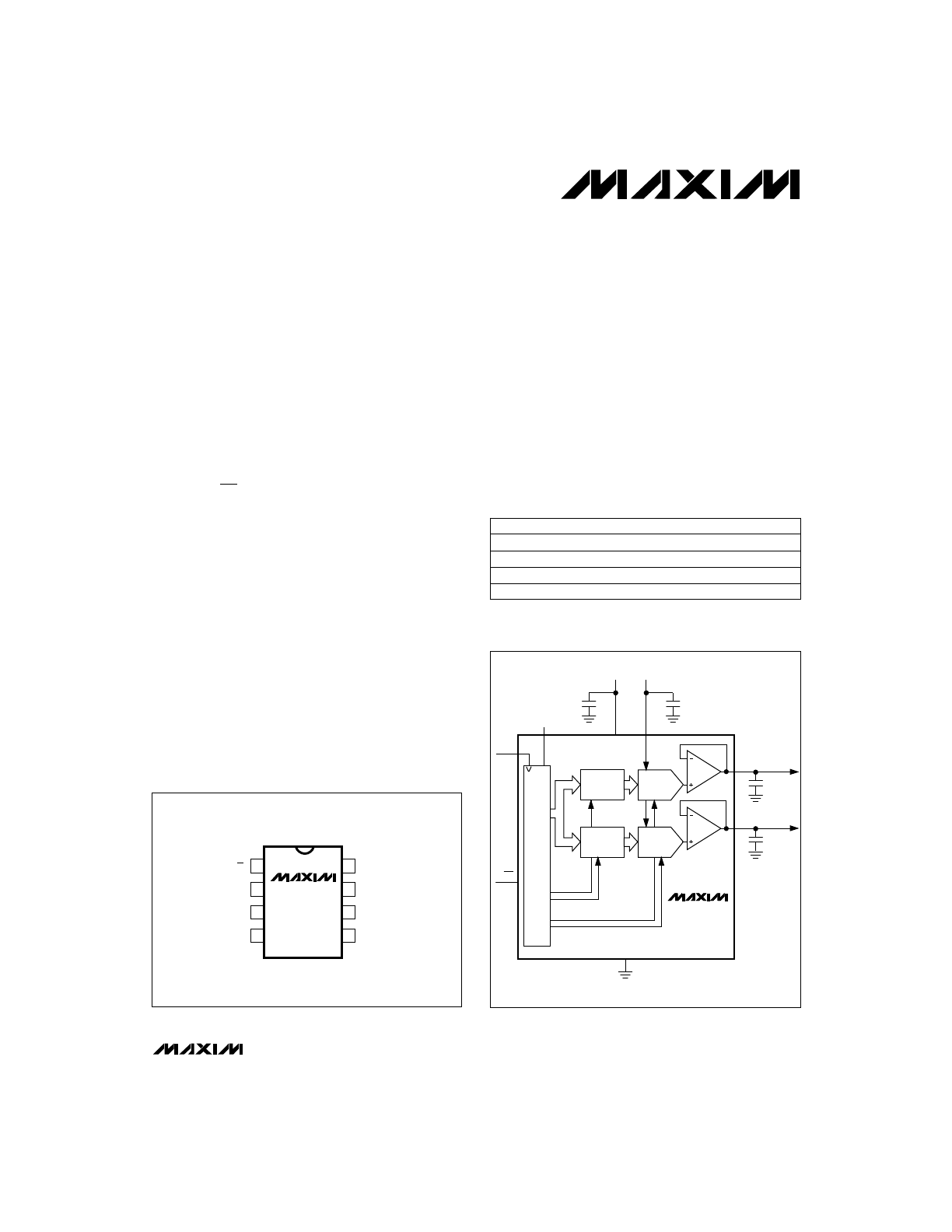
MAX522
Dual, 8-Bit, Voltage-Output
Serial DAC in 8-Pin SO Package
________________________________________________________________
Maxim Integrated Products
1
DAC
LATCH
A
DAC A
DAC
LATCH
B
DAC B
SCLK
OUTA
OUTB
DIN
REF
V
DD
CS
16-BIT SHIFT REGISTER
CONTROL (8)
DATA (8)
MAX522
8
3
1
5
6
7
2
0.1
µ
F
0.1
µ
F
(OPTIONAL)
0.01
µ
F
V
OUTA
V
OUTB
GND
4
0.22
µ
F
________________Functional Diagram
OUTB
V
DD
OUTA
GND
1
2
8
7
DIN
REF
SCLK
CS
MAX522
TOP VIEW
3
4
6
5
DIP/SO
__________________Pin Configuration
Call toll free 1-800-998-8800 for free samples or literature.
19-0403; Rev 0; 6/95
PART
TEMP. RANGE
PIN-PACKAGE
MAX522CPA
0°C to +70°C
8 Plastic DIP
MAX522CSA
0°C to +70°C
8 SO
MAX522EPA
-40°C to +85°C
8 Plastic DIP
SPI and QSPI are trademarks of Motorola Inc.
Microwire is a trademark of National Semiconductor Corp.
______________Ordering Information
MAX522ESA
-40°C to +85°C
8 SO
MAX522
Dual, 8-Bit, Voltage-Output
Serial DAC in 8-Pin SO Package
2
_______________________________________________________________________________________
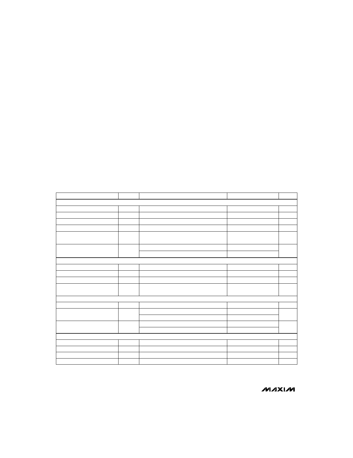
ABSOLUTE MAXIMUM RATINGS
ELECTRICAL CHARACTERISTICS
(V
DD
= +2.7V to +5.5V, REF = V
DD
, T
A
= T
MIN
to T
MAX
, unless otherwise noted. Typical values are at T
A
= +25°C.)
Note 1:
The outputs may be shorted to V
DD
or GND if the package power dissipation is not exceeded. Typical short-circuit current to
GND is 50mA.
Stresses beyond those listed under “Absolute Maximum Ratings” may cause permanent damage to the device. These are stress ratings only, and functional
operation of the device at these or any other conditions beyond those indicated in the operational sections of the specifications is not implied. Exposure to
absolute maximum rating conditions for extended periods may affect device reliability.
V
DD
to GND ................................................................ -0.3V, +6V
Digital Inputs and Outputs to GND............... -0.3V, (V
DD
+ 0.3V)
REF ................................................................-0.3V, (V
DD
+ 0.3V)
OUTA, OUTB (Note 1)............................................................V
DD
Continuous Power Dissipation (T
A
= +70°C)
Plastic DIP (derate 9.09mW/°C above +70°C) ..............727mW
SO (derate 5.88mW/°C above +70°C) ...........................471mW
Operating Temperature Ranges
MAX522C_ A.......................................................0°C to +70°C
MAX522E_ A....................................................-40°C to +85°C
Storage Temperature Range .............................-65°C to +165°C
Lead Temperature (soldering, 10sec) .............................+300°C
(Note 3)
2.7V
≤
V
DD
≤
3.6V, REF = 2.4V
4.5V
≤
V
DD
≤
5.5V, REF = 4.096V
CONDITIONS
M
Ω
2
Reference Input Resistance
(shutdown mode)
k
Ω
R
REF
Reference Input Resistance
8
pF
25
Reference Input Capacitance
GND
V
DD
%/%
0.01
PSRR
Power-Supply Rejection Ratio
Bits
8
N
Resolution
µV/°C
100
Zero-Code Temperature
Coefficient
UNITS
MIN
TYP
MAX
SYMBOL
PARAMETER
Guaranteed monotonic
LSB
±1
DNL
Differential Nonlinearity
0.015
(Note 2)
LSB
±1.5
INL
Integral Nonlinearity
(Note 2)
LSB
±1
TUE
Total Unadjusted Error
Reference Input Voltage Range
V
DAC A
µF
0.1
Capacitive Load at OUT_
DAC A
Ω
50
Output Resistance
V
0
REF
Output Voltage Range
V
(0.7)(V
DD
)
V
IH
Input High Voltage
V
(0.3)(V
DD
)
V
IL
Input Low Voltage
V
IN
= 0V or V
DD
µA
0.1
±10
I
IN
Input Current
(Notes 4, 5)
pF
10
C
IN
Input Capacitance
DAC B
DAC B
0.01
500
STATIC PERFORMANCE
REFERENCE INPUTS
DAC OUTPUTS
DIGITAL INPUTS
MAX522
Dual, 8-Bit, Voltage-Output
Serial DAC in 8-Pin SO Package
_______________________________________________________________________________________
3
Note 2:
Reduced digital code range (code 24 through code 232) is due to swing limitations of the output amplifiers. See
Typical
Operating Characteristics.
Note 3:
Reference input resistance is code dependent. The lowest input resistance occurs at code 55hex. Refer to the
Reference
Input section in the Detailed Description.
Note 4:
Guaranteed by design. Not production tested.
Note 5:
Input capacitance is code dependent. The highest capacitance occurs at code 00hex.
CONDITIONS
UNITS
MIN
TYP
MAX
SYMBOL
PARAMETER
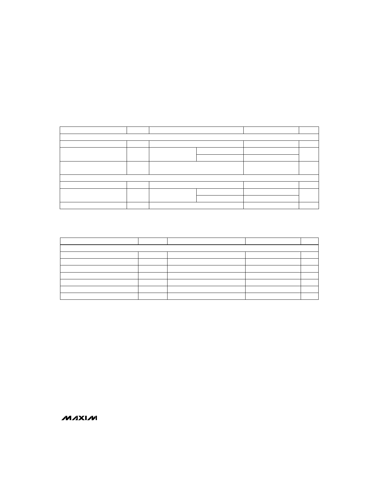
ELECTRICAL CHARACTERISTICS (continued)
(V
DD
= +2.7V to +5.5V, REF = V
DD
, T
A
= T
MIN
to T
MAX
, unless otherwise noted. Typical values are at T
A
= +25°C.)
Voltage-Output Slew Rate
SR
C
L
= 0.1µF (DAC A), C
L
= 0.01µF (DAC B)
0.1
V/µs
70
Voltage-Output Settling Time
To ±
1
⁄
2
LSB
µs
Digital Feedthrough
and Crosstalk
All 0s to all 1s
10
nV-s
Supply Voltage Range
V
DD
2.7
5.5
V
Shutdown Supply Current
V
DD
= 5.5V
0.1
µA
C
L
= 0.1µF (DAC A)
C
L
= 0.01µF (DAC B)
70
Supply Current
I
DD
All inputs = 0V
1.3
2.8
mA
0.9
2.5
DYNAMIC PERFORMANCE
POWER SUPPLIES
V
DD
= 5.5V
V
DD
= 3.6V
TIMING CHARACTERISTICS (Note 4)
(V
DD
= +2.7V to +5.5V, T
A
= T
MIN
to T
MAX
, unless otherwise noted.)
CONDITIONS
ns
200
t
CSPWH
–
C
—
S
–
Pulse Width High
ns
100
t
CL
SCLK Pulse Width Low
ns
100
t
CH
SCLK Pulse Width High
ns
50
t
DH
DIN to SCLK Rise Hold Time
ns
50
t
DS
DIN to SCLK Rise Setup Time
UNITS
MIN
TYP
MAX
SYMBOL
PARAMETER
ns
150
t
CSS
–
C
—
S
–
Fall to SCLK Rise Setup Time
ns
150
t
CSH
SCLK Rise to
–
C
—
S
–
Rise Setup Time
SERIAL INTERFACE TIMING
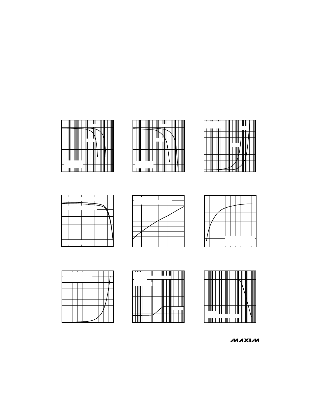
0
0.5
-60
80
120 140
SHUTDOWN SUPPLY CURRENT
vs. TEMPERATURE
1.0
1.5
4.0
4.5
MAX522 TOC-07
TEMPERATURE (°C)
SHUTDOWN SUPPLY CURRENT (
µ
A)
40
3.0
2.5
2.0
-40
0
100
60
-20
20
3.5
REF = V
DD
= 5V
ALL LOGIC INPUTS = 5V
ALL DACs SET TO ALL 1s
0.01
10
1
1000
0.1
100
REFERENCE FEEDTHROUGH
vs. FREQUENCY
-100
MAX522 TOC-08
FREQUENCY (kHz)
FEEDTHROUGH (dB)
-60
-20
-120
-80
-40
0
DAC A, B
V
DD
= 3V
V
REF
= 0V TO 2.9V SINE WAVE
NO LOAD
CODE = ALL 0s
0.001
1
1000
0.1
100
0.01
10
REFERENCE LARGE-SIGNAL
FREQUENCY RESPONSE
-20
MAX522 TOC-09
FREQUENCY (kHz)
RELATIVE OUTPUT (dB)
-10
0
-25
-15
-5
5
V
DD
= 3V
V
REF
= 0V TO V
DD
SINE WAVE
MAX522
Dual, 8-Bit, Voltage-Output
Serial DAC in 8-Pin SO Package
4
_______________________________________________________________________________________
__________________________________________Typical Operating Characteristics
(T
A
= +25°C, unless otherwise noted.)
0.0001
0.1
100
0.01
10
0.001
1
OUTPUT VOLTAGE vs.
OUTPUT SOURCE CURRENT (V
DD
= 3V)
0.5
MAX522 TOC-01
OUTPUT SOURCE CURRENT (mA)
OUTPUT VOLTAGE (V)
1.5
2.5
3.5
0
1.0
2.0
3.0
DAC A
DAC B
REF = V
DD
= 3V
CODE = ALL 1s
0
-35
0
192 224 255
TOTAL UNADJUSTED ERROR
vs. DIGITAL CODE
-30
-10
-5
MAX522 TOC-04
DIGITAL CODE
TUE (LSB)
96
128
160
-20
-25
32
64
-15
REF = V
DD
= 3V
DAC A LOADED WITH 5mA
DAC B LOADED WITH 0.5mA
0.0001
0.1
100
0.01
10
0.001
1
OUTPUT VOLTAGE vs.
OUTPUT SOURCE CURRENT (V
DD
= 5V)
3.8
MAX522 TOC-02
OUTPUT SOURCE CURRENT (mA)
OUTPUT VOLTAGE (V) 4.2
4.6
5.0
5.2
4.0
4.4
4.8
DAC A
DAC B
REF = V
DD
= 5V
CODE = ALL 1s
0.0001
0.1
100
0.01
10
0.001
1
OUTPUT VOLTAGE vs.
OUTPUT SINK CURRENT
100
MAX522 TOC-03
OUTPUT SINK CURRENT (mA)
OUTPUT VOLTAGE (mV)
300
500
700
800
900
0
200
400
600
DAC A
DAC B
REF = V
DD
= 3V
CODE = ALL 1s
1.2
0.5
2.5
4.5
5.0
5.5
POSITIVE SUPPLY CURRENT
vs. SUPPLY VOLTAGE
0.6
1.0
1.1
1.5
1.3
1.4
MAX522 TOC-05
V
DD
(V)
I
DD
(mA)
4.0
0.8
0.7
3.0
3.5
0.9
REF = V
DD
ALL LOGIC INPUTS GROUNDED
1.340
-60
80
120 140
POSITIVE SUPPLY CURRENT
vs. TEMPERATURE
1.345
1.365
1.370
MAX522 TOC-06
TEMPERATURE (°C)
I
DD
(mA)
40
1.355
1.350
-40
0
100
60
-20
20
1.360
REF = V
DD
= 5V
ALL LOGIC INPUTS = 5V
ALL DACs SET TO ALL 1s
MAX522
Dual, 8-Bit, Voltage-Output
Serial DAC in 8-Pin SO Package
_______________________________________________________________________________________
5
100k
10k
1k
0.1k
1M
10M
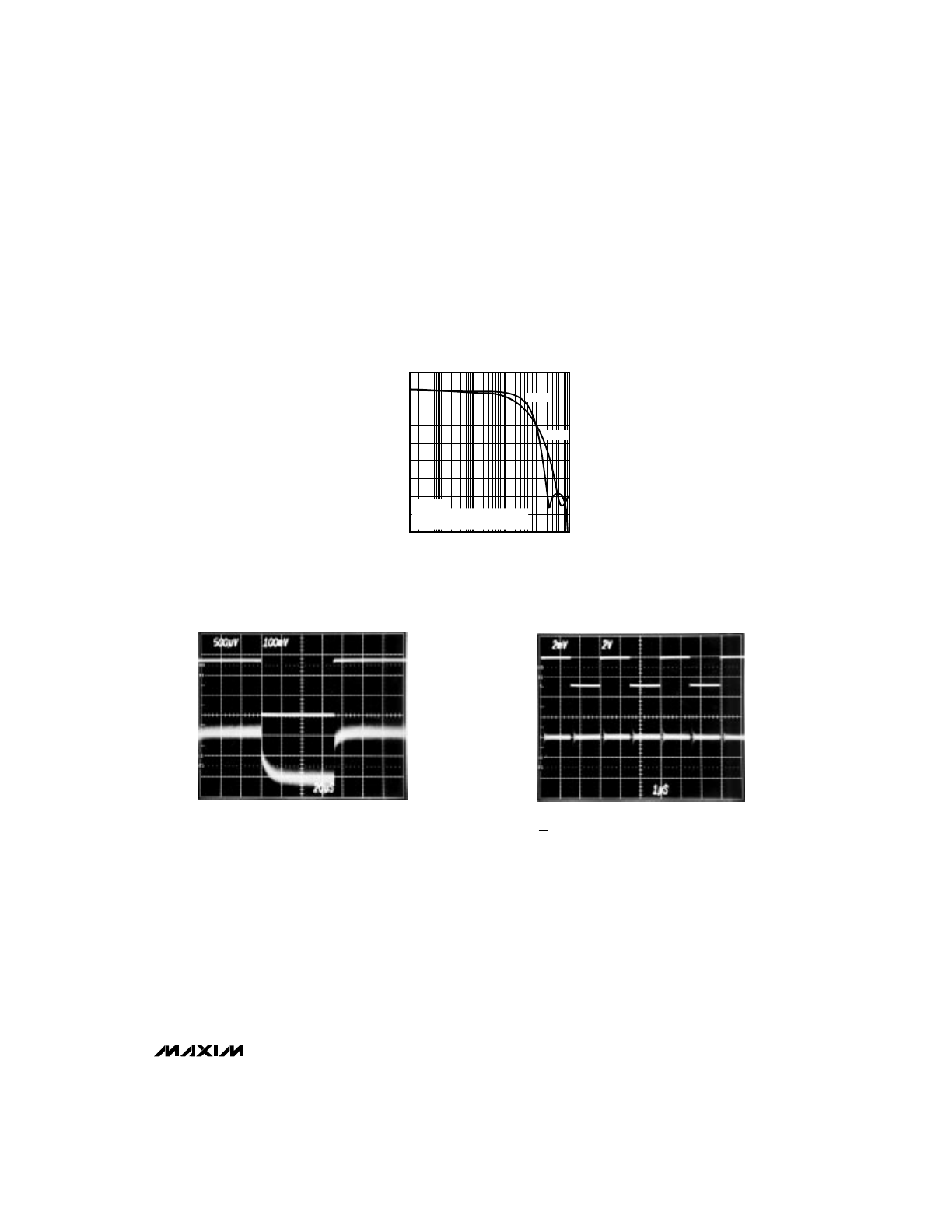
REFERENCE SMALL-SIGNAL
FREQUENCY RESPONSE
-80
MAX522 TOC-10
FREQUENCY (Hz)
RELATIVE OUTPUT (dB)
-40
0
-60
-20
DAC A
DAC B
V
DD
= 3V
V
REF
= 1.5V DC WITH ±40mV
P-P
SINE WAVE SUPERIMPOSED
____________________________Typical Operating Characteristics (continued)
(T
A
= +25°C, unless otherwise noted.)
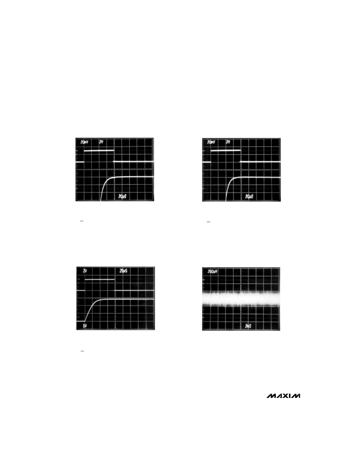
3.14V
LINE-TRANSIENT RESPONSE (OUTA)
2.86V
20
µ
s/div
A : V
DD,
100mV/div
B : OUTA, 500
µ
V/div
REF = 2.56V, NO LOAD, CODE = ALL 1s
A
B
CLOCK FEEDTHROUGH (OUTA)
B
1
µ
s/div
A
A: SCLK, 333kHz, 0V TO 2.9V, 2V/div
B: OUTA, 2mV/div
CS = HIGH
MAX522
Dual, 8-Bit, Voltage-Output
Serial DAC in 8-Pin SO Package
6
_______________________________________________________________________________________
____________________________Typical Operating Characteristics (continued)
(T
A
= +25°C, unless otherwise noted).
A
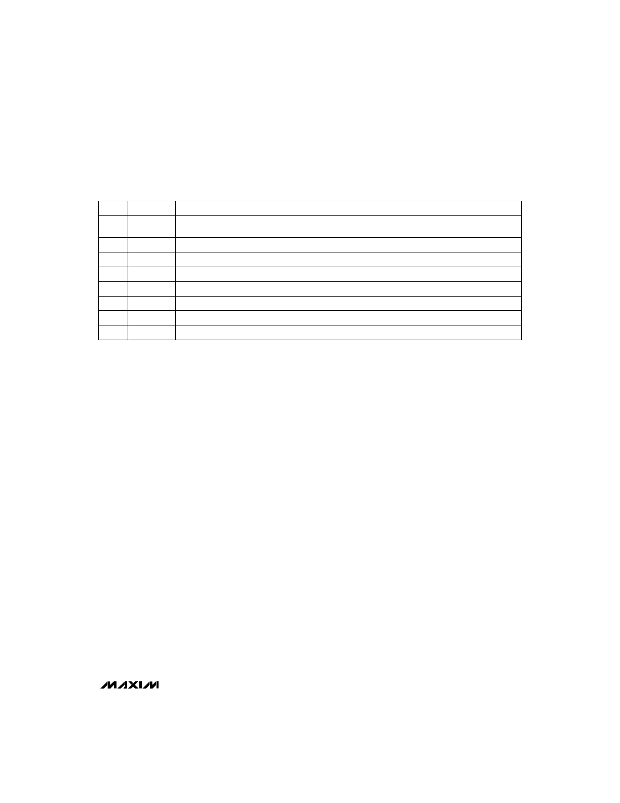
POSITIVE SETTLING TIME (DAC A)
20
µ
s/div
V
DD
= 3V, REF = V
DD,
R
L
= 1k
Ω
, C
L
= 0.1
µ
F,
ALL BITS OFF TO ALL BITS ON
B
A: CS, 2V/div
B: OUTA, 20mV/div
A
POSITIVE SETTLING TIME (DAC B)
20
µ
s/div
V
DD
= 3V, REF = V
DD,
R
L
= 10k
Ω
, C
L
= 0.01
µ
F,
ALL BITS OFF TO ALL BITS ON
B
A: CS, 2V/div
B: OUTB, 20mV/div
A
TIME EXITING SHUTDOWN MODE
20
µ
s/div
V
DD
= 3V, REF = V
DD,
R
L
= 1k
Ω
, C
L
= 0.1
µ
F,
DAC LOADED WITH ALL 1s
B
A: CS, 2V/div
B: OUTA, 1V/div
OUTA
200
µ
V/div
OUTPUT VOLTAGE NOISE (DC TO 1MHz)
2ms/div
DIGITAL CODE = 80, REF = V
DD,
NO LOAD
MAX522
Dual, 8-Bit, Voltage-Output
Serial DAC in 8-Pin SO Package
_______________________________________________________________________________________
7
_______________Detailed Description
Analog Section
The MAX522 contains two 8-bit, voltage-output digital-
to-analog converters (DACs). The DACs are “inverted”
R-2R ladder networks using complementary switches
that convert 8-bit digital inputs into equivalent analog
output voltages in proportion to the applied reference
voltage.
The MAX522 has one reference input which is shared
by DAC A and DAC B. The device includes output
buffer amplifiers for both DACs and input logic for sim-
ple microprocessor (µP) and CMOS interfaces. The
power-supply range is from +5.5V down to +2.7V.
Reference Input and DAC Output Range
The voltage at REF sets the full-scale output of the
DACs. The input impedance of the REF input is code
dependent. The lowest value, approximately 8k
Ω
,
occurs when the input code is 01010101 (55hex). The
maximum value of infinity occurs when the input code
is zero.
In shutdown mode, the selected DAC output is set to
zero while the value stored in the DAC register remains
unchanged. This removes the load from the reference
input to save power. Bringing the MAX522 out of shut-
down mode restores the DAC output voltage. Because
the input resistance at REF is code dependent, the
DAC’s reference sources should have an output
impedance of no more than 5
Ω
. The input capacitance
at the REF pin is also code dependent and typically
does not exceed 25pF.
The reference voltage on REF can range anywhere from
GND to V
DD
. See the
Output Buffer Amplifier section for
more information.
Output Buffer Amplifiers
DAC A and DAC B voltage outputs are internally
buffered. The buffer amplifiers have a rail-to-rail
(GND to V
DD
) output voltage range.
The DAC outputs are internally divided by two and the
buffer is set to a gain of two, eliminating the need for a
buffer input voltage range to the positive supply rail.
DAC A’s output amplifier can source and sink up to
5mA of current (0.5mA for DAC B’s buffer). See the
Total Unadjusted Error vs. Digital Code graph in the
Typical Operating Characteristics. The amplifier is
unity-gain stable with a capacitive load of 0.1µF
(0.01µF for DAC B’s buffer) or greater. The slew rate is
limited by the load capacitor and is typically 0.1V/µs
with a 0.1µF load (0.01µF for DAC B’s buffer).
Shutdown Mode
When programmed to shutdown mode, the outputs of
DAC A and DAC B go into a high-impedance state.
Virtually no current flows into or out of the buffer ampli-
fiers in that state. In shutdown mode, the REF inputs
are high impedance (2M
Ω
typical) to conserve current
drain from the system reference; therefore, the system
reference does not have to be powered down.
Coming out of shutdown, the DAC outputs return to the
values kept in the registers. The recovery time is equiv-
alent to the DAC settling time.
______________________________________________________________Pin Description
NAME
FUNCTION
1
–
C
—
S
–
Chip Select (active low). Enables data to be shifted into the 16-bit shift register. Programming commands
are executed at the rising edge of
–
C
—
S
–
.
2
SCLK
Serial Clock Input. Data is clocked in on the rising edge of SCLK.
PIN
3
V
DD
Positive Power Supply (2.7V to 5.5V). Bypass with 0.22µF to GND.
4
GND
Ground
8
DIN
Serial Data Input of the 16-bit shift register. Data is clocked into the register on the rising edge of SCLK.
7
REF
Reference Input for DAC A and DAC B
6
OUTB
DAC B Output Voltage (Buffered).
Connect 0.01µF capacitor or greater to GND.
5
OUTA
DAC A Output Voltage (Buffered).
Connect 0.1µF capacitor or greater to GND.
MAX522
Dual, 8-Bit, Voltage-Output
Serial DAC in 8-Pin SO Package
8
_______________________________________________________________________________________
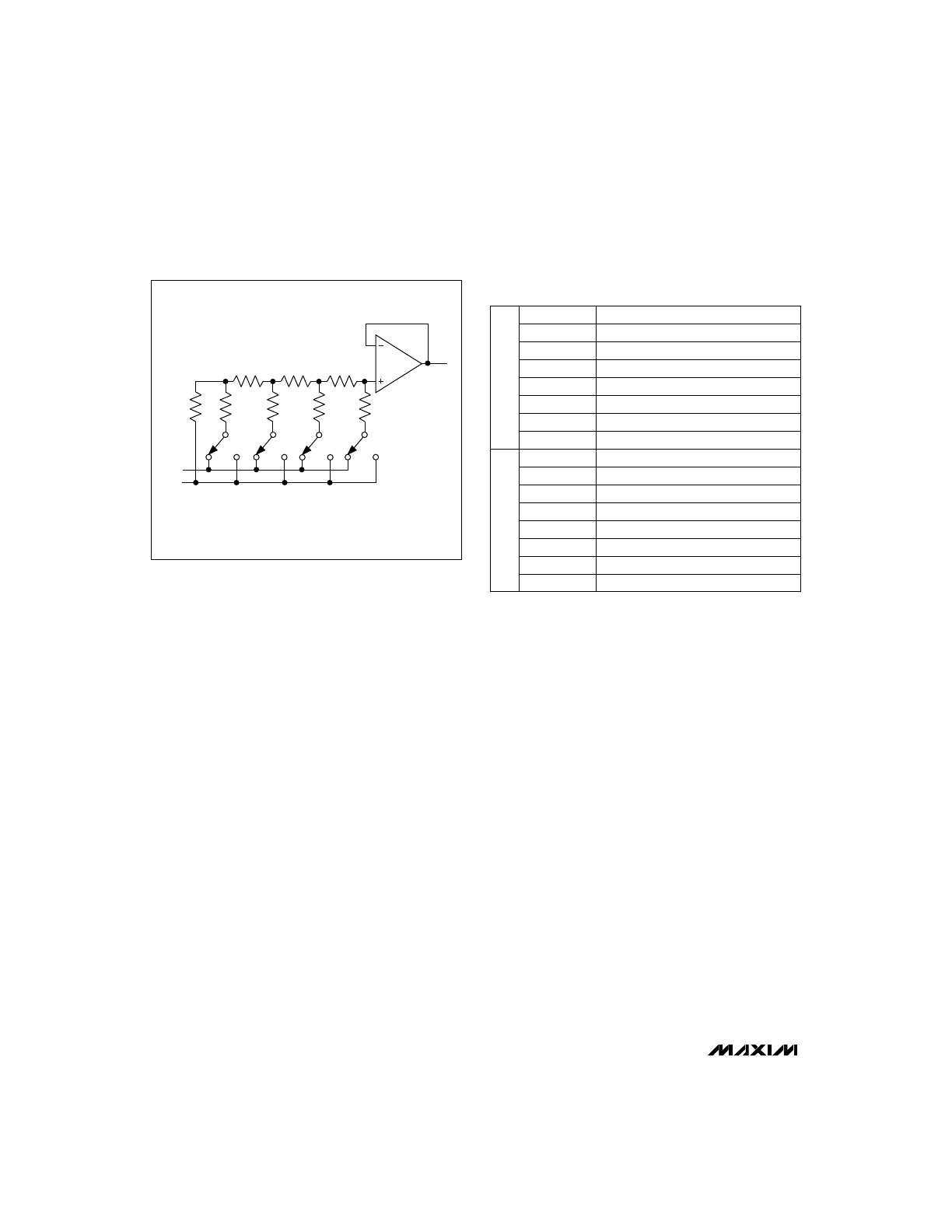
Figure 1. DAC Simplified Circuit Diagram
2R
2R
2R
2R
2R
R
R
R
REF
GND
OUT
SHOWN FOR ALL 1s ON DAC
Table 1. Input Shift Register
*
*
Clocked in last.
**Clocked in first.
Uncommitted Bit 1
UB1**
Uncommitted Bit 2
UB2
Uncommitted Bit 3
UB3
Shut Down DAC B, Active High
SB
Shut Down DAC A, Active High
SA
Uncommitted Bit 4
UB4
Load Reg DAC B, Active High
LB
Load Reg DAC A, Active High
LA
DAC Data Bit 7 (MSB)
B7
DAC Data Bit 6
B6
DAC Data Bit 5
B5
DAC Data Bit 4
B4
DAC Data Bit 3
B3
DAC Data Bit 2
B2
DAC Data Bit 1
B1
DAC Data Bit 0 (LSB)
B0*
DATA BITS
CONTROL BITS
Serial Interface
An active-low chip select (
–
C
—
S
–
) enables the shift register
to receive data from the serial data input. Data is
clocked into the shift register on every rising edge of
the serial clock signal (SCLK). The clock frequency can
be as high as 5MHz.
Data is sent MSB first and can be transmitted in one 16-
bit word. The write cycle can be segmented when
–
C
—
S
–
is
kept active (low) to allow, for example, two 8-bit-wide
transfers. After clocking all 16 bits into the input shift
register, the rising edge of
–
C
—
S
–
updates the DAC outputs
and the shutdown status. Because of their single
buffered structure, DACs cannot be simultaneously
updated to different digital values.
Serial-Input Data Format and Control Codes
Table 2 lists the serial-input data format. The 16-bit
input word consists of an 8-bit control byte and an 8-bit
data byte. The 8-bit control byte is not decoded inter-
nally. Every control bit performs one function. Data is
clocked in starting with UB1 (Uncommitted Bit), fol-
lowed by the remaining control bits and the data byte.
The LSB of the data byte (B0) is the last bit clocked into
the shift register (Figure 2).
Table 3 is an example of a 16-bit input word. It per-
forms the following functions:
• 80hex (128 decimal) loaded into DAC registers
A and B.
• DAC A and DAC B are active.
MAX522
Dual, 8-Bit, Voltage-Output
Serial DAC in 8-Pin SO Package
_______________________________________________________________________________________
9
DIN
SCLK
CS
UB1 UB2 UB3
SB
SA
UB4
LB
LA
D7
D6
D5
D4
D3
D2
D1
D0
OPTIONAL
INSTRUCTION
EXECUTED
(CONTROL BYTE)
(DATA BYTE)
Figure 2. MAX522 3-Wire Serial-Interface Timing Diagram
Table 2. Serial-Interface Programming Commands
Table 3. Example of a 16-Bit Input Word
X =
Don’t care.
* = Not shown, for the sake of clarity. The functions of loading and shutting down the DACs and programming the logic can be combined in a single
command.
X
X
1
0
0
0
1
1
1
0
0
0
0
0
0
0
UB1
UB2
UB3
SB
SA
UB4
LB
LA
B7
B6
B5
B4
B3
B2
B1
B0
Loaded
Loaded
in First
in Last
CONTROL
*
1
1
*
0
X
X
1
X
0
*
1
1
X
X
X
X
X
0
*
0
1
0
0
1
0
0
1
B6
B5
Shut Down All DACs
X
X
X
X
X
X
X
X
*
*
0
1
1
1
X
X
Shut Down DAC A
X
X
X
X
X
X
X
X
*
*
0
1
0
1
X
X
Shut Down DAC B
X
X
X
X
X
X
X
X
*
*
0
0
1
1
X
X
Unassigned Command
X
X
X
X
X
X
X
X
*
*
0
0
0
1
X
X
All DACs Active
X
X
X
X
X
X
X
X
*
*
0
0
0
1
X
X
Load Both DAC Registers
8-Bit DAC Data
*
Load Register to DAC A
8-Bit DAC Data
*
Load Register to DAC B
8-Bit DAC Data
*
Unassigned Command
*
No Operation to DAC Registers
X
X
X
X
X
X
X
X
0
0
0
*
*
1
X
X
FUNCTION
B0
LSB
B1
B2
B3
B4
B7
MSB
LA
LB
UB4
SA
SB
UB3
UB2
UB1
DATA
Digital Inputs
The digital inputs are compatible with CMOS logic.
Supply current increases slightly when toggling the
logic inputs through the transition zone between
(0.3)(V
DD
) and (0.7)(V
DD
).
Microprocessor Interfacing
The MAX522 serial interface is compatible with
Microwire, SPI, and QSPI. For SPI, clear the CPOL and
CPHA bits (CPOL = 0 and CPHA = 0). CPOL = 0 sets
the inactive clock state to zero and CPHA = 0 changes
data at the falling edge of SCLK. This setting allows SPI
to run at full clock speeds (0.5MHz). If a serial port is
not available on your µP, three bits of a parallel port can
be used to emulate a serial port by bit manipulation.
Minimize digital feedthrough at the voltage outputs by
operating the serial clock only when necessary.
MAX522
Dual, 8-Bit, Voltage-Output
Serial DAC in 8-Pin SO Package
10
______________________________________________________________________________________
1LSB
REF
2
REF
1
256
ANALOG OUTPUT
REF
D
256
8
=
×
=
×
=
×
−
Table 4. Code Table
CS
SCLK
DIN
t
DS
t
DH
t
CL
t
CH
t
CSS
t
CSPWH
t
CSH
Figure 3. MAX522 Detailed Serial-Interface Timing Diagram
0V
0
0
0
0
0
0
0
0
+
×
REF
1
256
1
0
0
0
0
0
0
0
+
×
REF
127
256
1
1
1
1
1
1
1
0
+
×
= +
REF
128
256
REF
2
0
0
0
0
0
0
0
1
+
×
REF
129
256
1
0
0
0
0
0
0
1
+
×
REF
255
256
1
1
1
1
1
1
1
1
ANALOG
OUTPUT
B0
B1
B2
B3
B4
B5
B6
B7
DAC CONTENTS
Note:
where D = Decimal
Value of Digital Input

MAX522
Dual, 8-Bit, Voltage-Output
Serial DAC in 8-Pin SO Package
______________________________________________________________________________________
11
______________
Applications Information
The MAX522 is specified for single-supply operation
with V
DD
ranging from 2.7V to 5.5V, covering all com-
monly used supply voltages in 3V and 5V systems.
Initialization
There is no internal power-on reset. Therefore, at
power-up, perform an initial write operation to set the
outputs to the desired voltage.
Power-Supply and
Ground Management
GND should be connected to the highest quality
ground available. Bypass V
DD
with a 0.1µF to 0.22µF
capacitor to GND. The reference input can be used
without bypassing. For optimum line/load-transient
response and noise performance, bypass the refer-
ence input with 0.1µF to 4.7µF to GND. Careful PC
board layout minimizes crosstalk among DAC outputs,
the reference, and digital inputs. Separate analog lines
with ground traces between them. Make sure that high-
frequency digital lines are not routed in parallel to ana-
log lines.
Maxim cannot assume responsibility for use of any circuitry other than circuitry entirely embodied in a Maxim product. No circuit patent licenses are
implied. Maxim reserves the right to change the circuitry and specifications without notice at any time.
12
__________________Maxim Integrated Products, 120 San Gabriel Drive, Sunnyvale, CA 94086 (408) 737-7600
© 1995 Maxim Integrated Products
Printed USA
is a registered trademark of Maxim Integrated Products.
MAX522
Dual, 8-Bit, Voltage-Output
Serial DAC in 8-Pin SO Package
________________________________________________________Package Information
DIM
A
A1
A2
A3
B
B1
C
D1
E
E1
e
eA
eB
L
MIN
–
0.015
0.125
0.055
0.016
0.045
0.008
0.005
0.300
0.240
0.100
0.300
–
0.115
MAX
0.200
–
0.175
0.080
0.022
0.065
0.012
0.080
0.325
0.310
–
–
0.400
0.150
MIN
–
0.38
3.18
1.40
0.41
1.14
0.20
0.13
7.62
6.10
2.54
7.62
–
2.92
MAX
5.08
–
4.45
2.03
0.56
1.65
0.30
2.03
8.26
7.87
–
–
10.16
3.81
INCHES
MILLIMETERS
Plastic DIP
PLASTIC
DUAL-IN-LINE
PACKAGE
(0.300 in.)
DIM
D
D
D
D
D
D
PKG.
P
P
P
P
P
N
MIN
0.348
0.735
0.745
0.885
1.015
1.14
MAX
0.390
0.765
0.765
0.915
1.045
1.265
MIN
8.84
18.67
18.92
22.48
25.78
28.96
MAX
9.91
19.43
19.43
23.24
26.54
32.13
INCHES
MILLIMETERS
PINS
8
14
16
18
20
24
C
A
A2
E1
D
E
eA
eB
A3
B1
B
0° - 15°
A1
L
D1
e
21-0043A
DIM
A
A1
B
C
E
e
H
L
MIN
0.053
0.004
0.014
0.007
0.150
0.228
0.016
MAX
0.069
0.010
0.019
0.010
0.157
0.244
0.050
MIN
1.35
0.10
0.35
0.19
3.80
5.80
0.40
MAX
1.75
0.25
0.49
0.25
4.00
6.20
1.27
INCHES
MILLIMETERS
21-0041A
Narrow SO
SMALL-OUTLINE
PACKAGE
(0.150 in.)
DIM
D
D
D
MIN
0.189
0.337
0.386
MAX
0.197
0.344
0.394
MIN
4.80
8.55
9.80
MAX
5.00
8.75
10.00
INCHES
MILLIMETERS
PINS
8
14
16
1.27
0.050
L
0°-8°
H
E
D
e
A
A1
C
0.101mm
0.004in.
B