
_______________General Description
The MAX520/MAX521 are quad/octal, 8-bit voltage-output
digital-to-analog converters (DACs) with simple 2-wire ser-
ial interfaces that allow communication between multiple
devices. They operate from a single +5V supply and their
reference input range includes both supply rails.
The MAX521 includes rail-to-rail output buffer amplifiers for
reduced system size and component count when driving
loads. The MAX520’s unbuffered voltage outputs reduce
the device’s total supply current to 4µA and provide
increased accuracy at low output currents.
The MAX520/MAX521 feature a serial interface and internal
software protocol, allowing communication at data rates up
to 400kbps. The interface, combined with the double-
buffered input configuration, allows the DAC registers to be
updated individually or simultaneously. In addition, the
devices can be put into a low-power shutdown mode that
reduces supply current to 4µA. Power-on reset ensures the
DAC outputs are at 0V when power is initially applied.
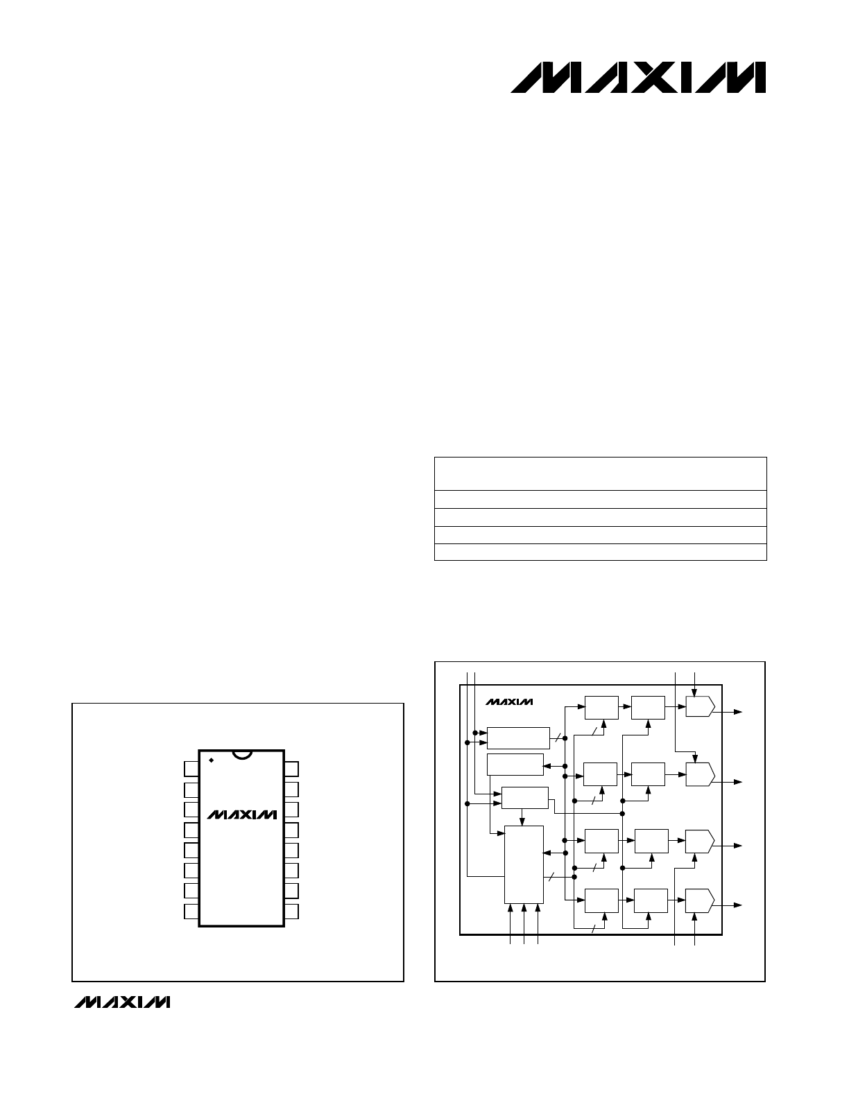
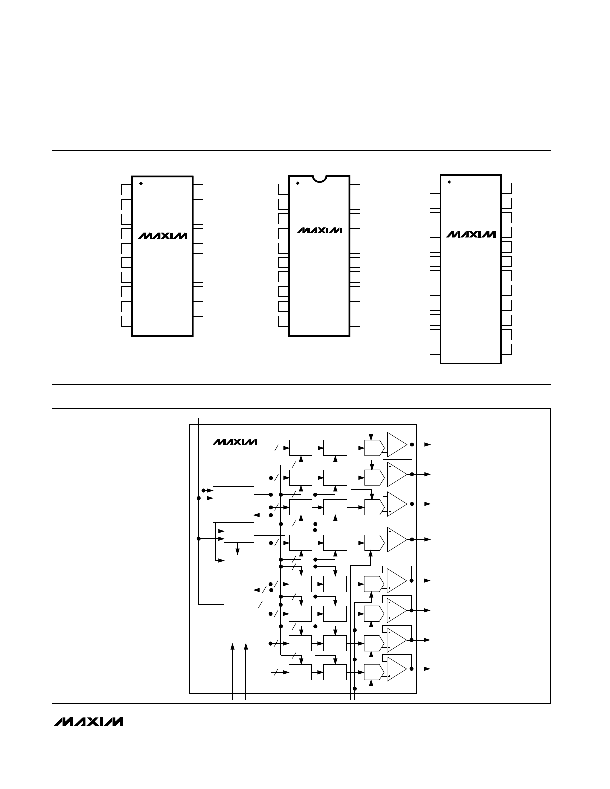
The MAX520 is available in 16-pin DIP and wide SO pack-
ages, as well as a space-saving 20-pin SSOP. The
MAX521 comes in 20-pin DIP and 24-pin SO packages, as
well as a space-saving 24-pin SSOP.
________________________Applications
Minimum Component Analog Systems
Digital Offset/Gain Adjustment
Industrial Process Control
Automatic Test Equipment
Programmable Attenuators
____________________________Features
♦
Single +5V Supply
♦
Simple 2-Wire Serial Interface
♦
I
2
C Compatible
♦
Outputs Swing Rail to Rail:
Unbuffered Outputs (MAX520)
Buffered Outputs (MAX521)
♦
1%-Accurate Trimmed Output Resistance (MAX520A)
♦
Ultra-Low 4µA Supply Current (MAX520)
♦
Individual DACs Have Separate Reference Inputs
♦
Power-On Reset Clears All Latches
♦
4µA Power-Down Mode
MAX520/MAX521
Quad/Octal, 2-Wire Serial 8-Bit DACs
with Rail-to-Rail Outputs
________________________________________________________________
Maxim Integrated Products
1
16
15
14
13
12
11
10
9
1
2
3
4
5
6
7
8
OUT1
OUT2
OUT3
REF2
REF3
V
DD
AD2
AD1
AD0
OUT0
REF1
REF0
AGND
DGND
SCL
SDA
TOP VIEW
MAX520
DIP/SO
_________________Pin Configurations
INPUT
LATCH 0
8-BIT
SHIFT REGISTER
SCL
REF0
SDA
REF1
OUTPUT
LATCH 0
DAC0
OUT0
1
MAX520
ADDRESS
COMPARATOR
START/STOP
DETECTOR
DECODE
OUTPUT
LATCH 1
DAC1
OUT1
4
8
INPUT
LATCH 2
OUTPUT
LATCH 2
DAC2
OUT2
OUT3
INPUT
LATCH 3
OUTPUT
LATCH 3
DAC3
REF3
REF2
AD2
AD1
AD0
1
INPUT
LATCH 1
1
1
_______________Functional Diagrams
______________Ordering Information
For free samples & the latest literature: http://www.maxim-ic.com, or phone 1-800-998-8800
19-0378; Rev 3; 9/96
PART
†
MAX520
ACPE
MAX520BCPE
MAX520ACWE
0°C to +70°C
0°C to +70°C
0°C to +70°C
TEMP. RANGE
PIN-PACKAGE
16 Plastic DIP
16 Plastic DIP
16 Wide SO
TUE
(LSB)
1
1
1
Pin Configurations continued at end of data sheet.
Functional Diagrams continued at end of data sheet.
MAX520BCWE
0°C to +70°C
16 Wide SO
1
Ordering Information continued at end of data sheet.
†
MAX520 “A” grade parts include a 1%-accurate, factory-trimmed
output resistance.
MAX520/MAX521
Quad/Octal, 2-Wire Serial 8-Bit DACs
with Rail-to-Rail Outputs
2
_______________________________________________________________________________________
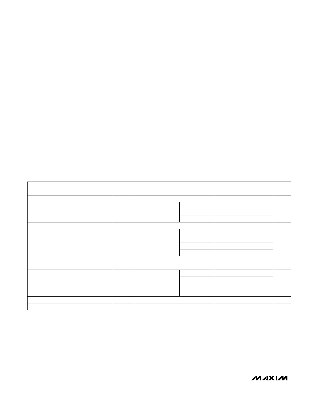
ABSOLUTE MAXIMUM RATINGS
ELECTRICAL CHARACTERISTICS
(V
DD
= 5V ±10%, V
REF_
= 4V, R
L
=
∞
(MAX520), R
L
= 10k
Ω
(MAX521), C
L
= 0pF (MAX520), C
L
= 100pF (MAX521), T
A
= T
MIN
to T
MAX,
unless otherwise noted. Typical values are at T
A
= +25°C)
Stresses beyond those listed under “Absolute Maximum Ratings” may cause permanent damage to the device. These are stress ratings only, and functional
operation of the device at these or any other conditions beyond those indicated in the operational sections of the specifications is not implied. Exposure to
absolute maximum rating conditions for extended periods may affect device reliability.
V
DD
to DGND ...........................................................-0.3V to +6V
V
DD
to AGND............................................................-0.3V to +6V
OUT_ ..........................................................-0.3V to (V
DD
+ 0.3V)
REF_ ...........................................................-0.3V to (V
DD
+ 0.3V)
AD0, AD1, AD2...........................................-0.3V to (V
DD
+ 0.3V)
SCL, SDA to DGND ..................................................-0.3V to +6V
AGND to DGND.....................................................-0.3V to +0.3V
Maximum Current into Any Pin............................................50mA
Continuous Power Dissipation (T
A
= +70°C)
16-Pin Plastic DIP (derate 10.53mW/°C above +70°C)....842mW
20-Pin Plastic DIP (derate 11.11mW/°C above +70°C)....889mW
16-Pin Wide SO (derate 9.52mW/°C above +70°C) ......762mW
24-Pin Wide SO (derate 11.76mW/°C above +70°C) ....941mW
20-Pin SSOP (derate 8.00mW/°C above +70°C) .........640mW
24-Pin SSOP (derate 8.00mW/°C above +70°C) .........640mW
16-Pin CERDIP (derate 10.00mW/°C above +70°C)....800mW
20-Pin CERDIP (derate 11.11mW/°C above +70°C)....889mW
Operating Temperature Ranges
MAX520_C_ _/MAX521_C_ _ ..............................0°C to +70°C
MAX520_E_ _/MAX521_E_ _ ...........................-40°C to +85°C
MAX520_MJE/MAX521BMJP ........................-55°C to +125°C
Storage Temperature Range .............................-65°C to +150°C
Lead Temperature (soldering, 10sec) .............................+300°C
CONDITIONS
Bits
8
Resolution
UNITS
MIN
TYP
MAX
SYMBOL
PARAMETER
±1.5
±1
18
Guaranteed monotonic
8
LSB
±1.0
DNL
LSB
±2
TUE
Total Unadjusted Error
Differential Nonlinearity
Code = 00 hex
Code = 00 hex
µV/°C
±10
mV
Code = 00 hex
±1
Zero-Code-Error Supply Rejection
Zero-Code-Error Temperature Coefficient
Code = FF hex
mV
20
20
Full-Scale Error
8
mV
20
ZCE
20
Zero-Code Error
Code = FF hex, V
DD
= 5V ±10%
µV/°C
±10
mV
±1
Full-Scale-Error Supply Rejection
Full-Scale-Error Temperature Coefficient
MAX520_
MAX520_
MAX521B
MAX521A
MAX521_C
MAX521_E
MAX521BM
MAX520_
18
MAX521_C
MAX521_E
MAX521BM
STATIC ACCURACY
MAX520/MAX521
Quad/Octal, 2-Wire Serial 8-Bit DACs
with Rail-to-Rail Outputs
_______________________________________________________________________________________
3
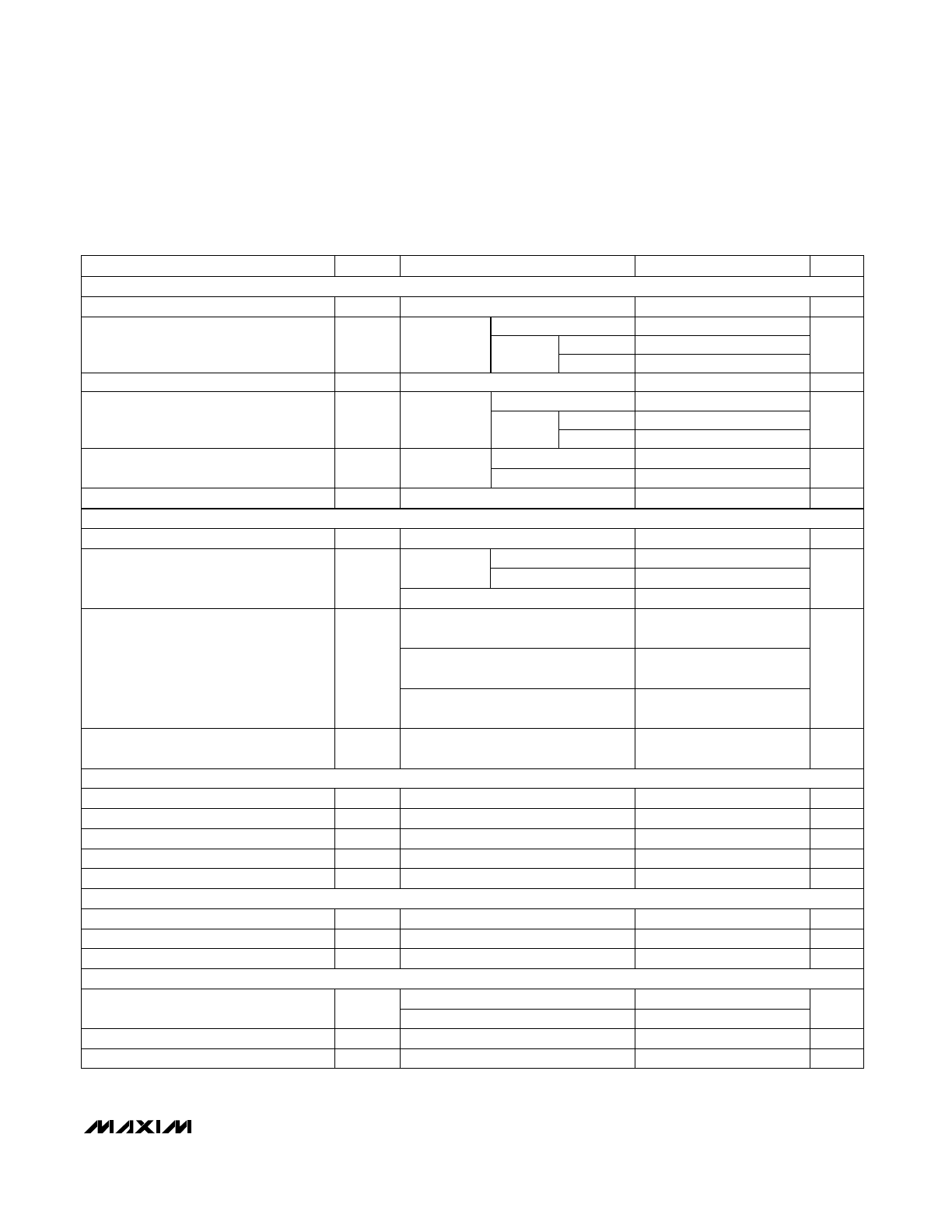
ELECTRICAL CHARACTERISTICS (continued)
(V
DD
= 5V ±10%, V
REF_
= 4V, R
L
=
∞
(MAX520), R
L
= 10k
Ω
(MAX521), C
L
= 0pF (MAX520), C
L
= 100pF (MAX521), T
A
= T
MIN
to T
MAX
,
unless otherwise noted. Typical values are at T
A
= +25°C)
(Note 3)
30
CONDITIONS
Input Capacitance
16
24
R
IN
Input Resistance
REF4
MAX520_
MAX521_
Input Current
-60
V
0
V
DD
Input Voltage Range
dB
-70
µA
±10
REF4
PD = 1
4
6
Code =
55 hex
(Note 1)
k
Ω
8
12
MAX520_
REF0–REF3
Channel-to-Channel Isolation
dB
-70
AC Feedthrough
120
Code =
FF hex
(Note 2)
pF
UNITS
MIN
TYP
MAX
SYMBOL
PARAMETER
30
MAX520_
REF0–REF3
15.8
16
16.2
V
0
V
DD
Full-Scale Output Voltage
k
Ω
8.4
16.4
Output Resistance (Note 5)
MAX521_, OUT_ = 4V,
0mA to 2.5mA
0.25
15.6
16
16.4
MAX521_, OUT_ = 0V to V
DD
,
PD = 1
µA
±10
Output Leakage Current
V
0.3V
DD
V
IL
Input Low Voltage
(Note 5)
V
0.05V
DD
V
HYST
Input Hysteresis
0V
≤
V
IN
≤
V
DD
µA
±10
I
IN
Input Current
V
0.7V
DD
V
IH
Input High Voltage
MAX521BM, V
REF_
= V
DD
,
code = FF hex, 0µA to 500µA
LSB
2.0
Output Load Regulation
(Note 5)
pF
10
C
IN
Input Capacitance
V
0.8
V
IL
Input Low Voltage
V
IN
= 0V to V
DD
µA
±10
I
IN
Input Leakage
V
2.4
V
IH
Input High Voltage
MAX520B
MAX521_C/E, V
REF_
= V
DD
,
code = FF hex, 0µA to 500µA
1.5
I
SINK
= 6mA
0.6
V
OL
Output Low Voltage
(Note 5)
pF
10
C
OUT
Three-State Output Capacitance
V
IN
= 0V to V
DD
µA
±10
I
L
Three-State Leakage Current
I
SINK
= 3mA
V
0.4
REFERENCE INPUTS
DIGITAL INPUTS SCL, SDA
DIGITAL INPUTS AD0, AD1
DIGITAL OUTPUT SDA
(Note 6)
(Note 4)
DAC OUTPUTS
MAX521_
MAX521_
MAX520A
T
A
= +25°C
T
A
= T
MIN
to T
MAX
MAX520/MAX521
Quad/Octal, 2-Wire Serial 8-Bit DACs
with Rail-to-Rail Outputs
4
_______________________________________________________________________________________
Note 1:
Input resistance is code dependent. The lowest input resistance occurs at code = 55 hex.
Note 2:
Input capacitance is code dependent. The highest input capacitance occurs at code = FF hex.
Note 3:
V
REF_
= 4Vp-p, 10kHz. Channel-to-channel isolation is measured by setting the code of one DAC to FF hex and setting the
code of all other DACs to 00 hex.
Note 4:
V
REF_
= 4Vp-p, 10kHz, DAC code = 00 hex.
Note 5:
Guaranteed by design.
Note 6:
I
2
C-compatible mode.
Note 7:
Output settling time is measured by taking the code from 00 hex to FF hex, and from FF hex to 00 hex.
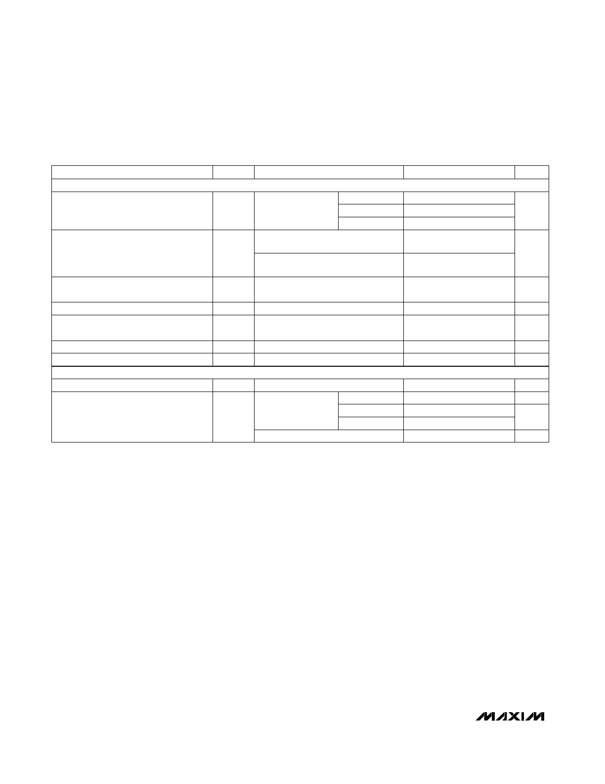
ELECTRICAL CHARACTERISTICS (continued)
(V
DD
= 5V ±10%, V
REF_
= 4V, R
L
=
∞
(MAX520), R
L
= 10k
Ω
(MAX521), C
L
= 0pF (MAX520), C
L
= 100pF (MAX521), T
A
= T
MIN
to T
MAX
,
unless otherwise noted. Typical values are at T
A
= +25°C)
MAX521BM
MAX521_C
0.7
MAX521_E
MAX520_
1.0
MAX521_C
MAX521_E/BM
Power-down mode (PD = 1)
10
20
4
20
Positive and negative
CONDITIONS
V/µs
0.5
Voltage Output Slew Rate
Operating mode, out-
put unloaded, all dig-
ital inputs 0V or V
DD
mA
4
20
I
DD
10
24
Supply Current
UNITS
MIN
TYP
MAX
SYMBOL
PARAMETER
MAX520_, to 1/2LSB, no load
µs
2
Output Settling Time
Code = 00 hex, all digital inputs from
0V to V
DD
nV-s
5
Digital Feedthrough
MAX521_, to 1/2LSB, 10k
Ω
and
100pF load (Note 7)
6
Code 128 to 127
nV-s
12
Digital-Analog Glitch Impulse
V
REF_
= 4Vp-p at 1kHz, V
DD
= 5V,
code = FF hex
dB
87
SINAD
Signal to Noise + Distortion Ratio
V
REF_
= 4Vp-p, 3dB bandwidth
MHz
1
Multiplying Bandwidth
MAX521_
µV
RMS
60
Wideband Amplifier Noise
V
4.5
5.5
V
DD
Supply Voltage
µA
µA
DYNAMIC PERFORMANCE
POWER REQUIREMENTS
MAX520/MAX521
Quad/Octal, 2-Wire Serial 8-Bit DACs
with Rail-to-Rail Outputs
_______________________________________________________________________________________
5
Note 8:
A master device must provide a hold time of at least 300ns for the SDA signal (referred to V
IL
of the SCL signal) in order to
bridge the undefined region of SCL’s falling edge.
Note 9:
Cb = total capacitance of one bus line in pF. t
R
and t
f
measured between 0.3V
DD
and 0.7V
DD
.
Note 10:
An input filter on the SDA and SCL input suppresses noise spikes less than 50ns.
Note 11:
Guaranteed by design.
Hold Time, (Repeated) Start Condition
t
HD, STA
0.6
µs
Low Period of the SCL Clock
t
LOW
1.3
µs
High Period of the SCL Clock
t
HIGH
0.6
PARAMETER
SYMBOL
MIN
TYP
MAX
UNITS
Serial Clock Frequency
f
SCL
0
400
kHz
Bus Free Time Between a STOP and a
START Condition
t
BUF
1.3
µs
CONDITIONS
µs
Setup Time for a Repeated START Condition
t
SU, STA
0.6
µs
Data Hold Time
t
HD, DAT
0
0.9
µs
Data Setup Time
t
SU, DAT
100
(Note 8)
ns
Fall Time of SDA Transmitting (Note 6)
t
F
20 + 0.1Cb
250
ns
Setup Time for STOP Condition
t
SU, STO
0.6
µs
Capacitive Load for Each Bus Line
Cb
400
I
SINK
≤
6mA (Note 9)
pF
Rise Time of Both SDA and SCL Signals, Receiving
t
R
20 + 0.1Cb
300
ns
Fall Time of Both SDA and SCL Signals, Receiving
t
F
20 + 0.1Cb
300
(Note 9)
(Note 9)
ns
Pulse Width of Spike Suppressed
t
SP
0
50
(Notes 10, 11)
ns
TIMING CHARACTERISTICS
(V
DD
= 5V ±10%, T
A
= T
MIN
to T
MAX
, unless otherwise noted. Typical values are at T
A
= +25°C.)
__________________________________________Typical Operating Characteristics
(V
DD
= 5V, DAC outputs unloaded, T
A
= +25°C, unless otherwise noted.)
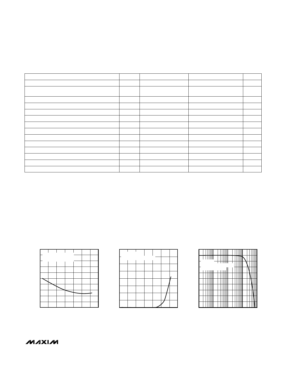
10
9
0
-60
-30
30
90
120
150
MAX520
SUPPLY CURRENT vs. TEMPERATURE
2
1
8
7
MAX520/521-01
TEMPERATURE (°C)
I
DD
(
µ
A)
0
60
6
5
4
3
OPERATING MODE OR
SHUTDOWN MODE
40
0
-60
-30
30
90
120
150
MAX520
REFERENCE INPUT CURRENT vs.
TEMPERATURE (SHUTDOWN MODE)
5
35
30
MAX520/521-02
TEMPERATURE (°C)
SHUTDOWN REFERENCE CURRENT (nA)
0
60
25
20
15
10
V
REF
= 4V
ONE REF INPUT DRIVEN
0
1k
100k
10k
1M
10M
MAX520
REFERENCE VOLTAGE INPUT
FREQUENCY RESPONSE
-16
-18
MAX520/521-03
FREQUENCY (Hz)
RELATIVE OUTPUT (dB)
-14
-12
-10
-8
-6
-4
-2
2
V
DD
= 5V
V
REF
= 4Vp-p SINE WAVE
CENTERED AT 2.5V
MAX520/MAX521
Quad/Octal, 2-Wire Serial 8-Bit DACs
with Rail-to-Rail Outputs
6
_______________________________________________________________________________________
______________________________Typical Operating Characteristics (continued)
(V
DD
= 5V, DAC outputs unloaded, T
A
= +25°C, unless otherwise noted.)
OUT2 = NO LOAD, REF2 = 4V,
DAC CODE = 00 HEX to FF HEX
1
µ
s/div
MAX520
POSITIVE SETTLING TIME
OUT2
1V/div
OUT2 = NO LOAD, REF2 = 4V,
DAC CODE = FF HEX to 00 HEX
1
µ
s/div
MAX520
NEGATIVE SETTLING TIME
OUT2
1V/div
REF2 = 4V, DAC CODE = 7F HEX to 80 HEX
500ns/div
MAX520
WORST-CASE 1LSB DIGITAL STEP CHANGE
(CAPACITIVE LOAD < 5pF)
OUT2
20mV/div
AC COUPLED
REF2 = 4V, DAC CODE = 7F HEX to 80 HEX
500ns/div
MAX520
WORST-CASE 1LSB DIGITAL STEP CHANGE
(CAPACITIVE LOAD = 25pF)
OUT2
20mV/div
AC COUPLED
MAX520/MAX521
Quad/Octal, 2-Wire Serial 8-Bit DACs
with Rail-to-Rail Outputs
_______________________________________________________________________________________
7
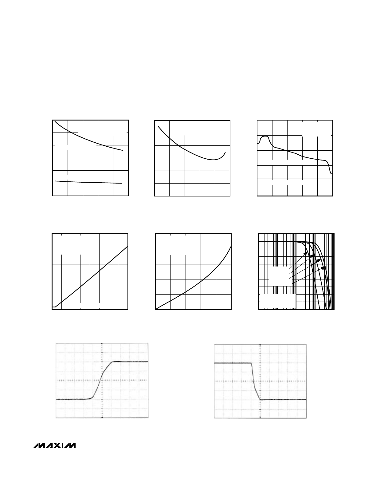
12
0
-60
-20
60
140
MAX521
SUPPLY CURRENT vs. TEMPERATURE
2
8
10
MAX520/521-08
TEMPERATURE (°C)
I
CC
(mA)
20
100
6
4
V
DD
= 5.5V
ALL REF INPUTS = 0.6V
ALL DIGITAL INPUTS to V
DD
ALL DAC CODES FF HEX
ALL DAC CODES 00 HEX
6
0
-60
-20
60
140
MAX521
SHUTDOWN SUPPLY CURRENT
vs. TEMPERATURE
1
4
5
MAX520/521-09
TEMPERATURE (°C)
SHUTDOWN I
CC
(
µ
A)
20
100
3
2
V
DD
= 5.5V
ALL REF INPUTS = 0.6V
ALL DIGITAL INPUTS to V
DD
10
0
0
1
3
5
MAX521
SUPPLY CURRENT
vs. REFERENCE VOLTAGE
2
6
8
MAX520/521-10
REFERENCE VOLTAGE (V)
I
CC
(mA)
2
4
4
ALL REFERENCE
INPUTS DRIVEN
ALL DAC CODES = FF HEX
ALL DAC CODES = 00 HEX
1.0
0
0
2
6
10
12
14
16
MAX521
DAC OUTPUT HIGH VOLTAGE
vs. OUTPUT SOURCE CURRENT
0.2
0.8
MAX520/521-11
OUTPUT SOURCE CURRENT (mA)
V
DD
- V
OUT
(V)
4
8
0.6
0.4
V
REF
= 5V
DAC CODE = FF HEX
LOAD to AGND
V
OUT
= V
REF
x (255/256)
1.0
0
0
2
6
10
MAX521
DAC OUTPUT LOW VOLTAGE
vs. OUTPUT SINK CURRENT
0.2
0.8
MAX520/521-12
OUTPUT SINK CURRENT (mA)
V
OUT
(V)
4
8
0.6
0.4
V
REF
= 5V
DAC CODE = 00 HEX
LOAD to V
DD
0
1k
100k
10k
1M
10M
MAX521
REFERENCE VOLTAGE INPUT
FREQUENCY RESPONSE
-16
-18
MAX520/521-13
FREQUENCY (Hz)
RELATIVE OUTPUT (dB)
-14
-12
-10
-8
-6
-4
-2
2
V
REF
= SINE WAVE
CENTERED AT 2.5V
4V
p-p
SINE
2V
p-p
SINE
1V
p-p
SINE
0.5V
p-p
SINE
__________________________________________Typical Operating Characteristics
(V
DD
= 5V, DAC outputs unloaded, T
A
= +25°C, unless otherwise noted.)
OUT1 LOADED WITH 10k
Ω
II 100pF, REF1 = 4V,
DAC CODE = 00 HEX to FF HEX
1
µ
s/div
MAX521
POSITIVE SETTLING TIME
OUT1
1V/div
OUT1 LOADED WITH 10k
Ω
II 100pF, REF1 = 4V,
DAC CODE = FF HEX to 00 HEX
1
µ
s/div
MAX521
NEGATIVE SETTLING TIME
OUT1
1V/div
MAX520/MAX521
Quad/Octal, 2-Wire Serial 8-Bit DACs
with Rail-to-Rail Outputs
8
_______________________________________________________________________________________
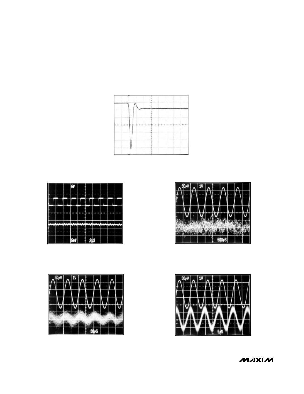
A = REF1, 1V/div (4V
P-P
)
B = OUT1, 50
µ
V/div, UNLOADED
FILTER PASSBAND = 1kHz to 100kHz, DAC CODE = 00 HEX
REFERENCE FEEDTHROUGH AT 10kHz
B
A
A = REF1, 1V/div (4V
P-P
)
B = OUT1, 50
µ
V/div, UNLOADED
FILTER PASSBAND = 10kHz to 1MHz, DAC CODE = 00 HEX
REFERENCE FEEDTHROUGH AT 100kHz
B
A
______________________________Typical Operating Characteristics (continued)
(V
DD
= 5V, DAC outputs unloaded, T
A
= +25°C, unless otherwise noted.)
REF1 = 5V, DAC CODE = 80 HEX to 7F HEX
500ns/div
MAX521
WORST-CASE 1LSB DIGITAL STEP CHANGE
OUT1
20mV/div
AC COUPLED
A = SCL, 400kHz, 5V/div
B = OUT1, 5mV/div
REF1 = 5V, DAC CODE = 7F HEX
CLOCK FEEDTHROUGH
B
A
A = REF1, 1V/div (4V
P-P
)
B = OUT1, 50
µ
V/div, UNLOADED
FILTER PASSBAND = 100Hz to 10kHz, DAC CODE = 00 HEX
REFERENCE FEEDTHROUGH AT 1kHz
B
A
MAX520/MAX521
Quad/Octal, 2-Wire Serial 8-Bit DACs
with Rail-to-Rail Outputs
_______________________________________________________________________________________
9
______________________________________________________________Pin Description
SCL
SDA
t
LOW
t
HIGH
t
F
t
R
t
HD
,
STA
t
HD
,
DAT
t
HD
,
STA
t
SU
,
DAT
t
SU
,
STA
t
BUF
t
SU
,
STO
START CONDITION
STOP CONDITION
REPEATED START CONDITION
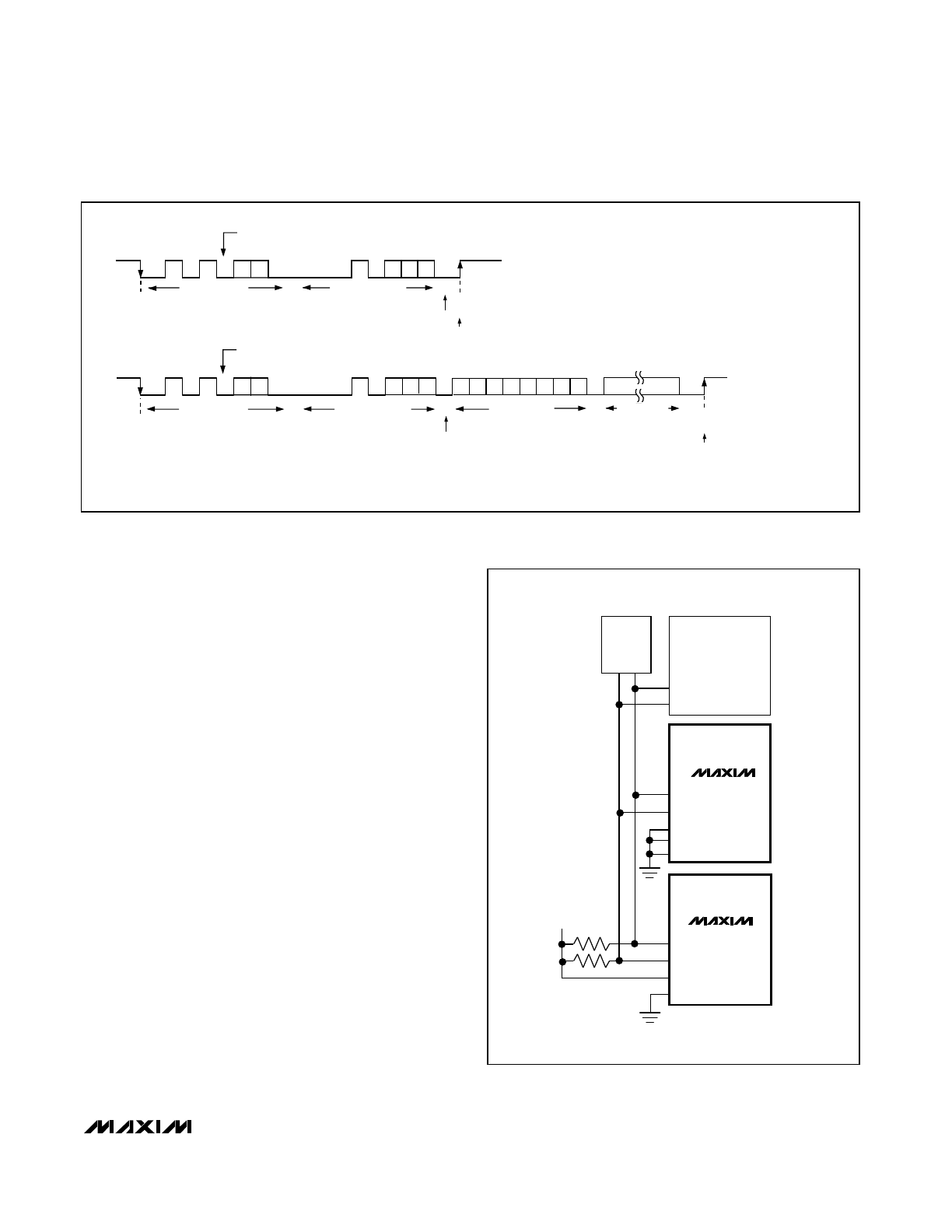
START CONDITION
Figure 1. 2-Wire Serial-Interface Timing Diagram
DIP
SO/SSOP
DIP/SO
SSOP
PIN
MAX521
NAME
MAX520
7
8
9
10
11
4
—
5
6
3
2
1
8
10
11
12
13
4
7, 9, 16, 20
5
6
3
2
1
12
13
14
15
14
15
17
18
16
19
17
18
19
20
21
22
23
24
Serial Clock Input
SCL
7
Serial Data Input
SDA
8
DAC4 Voltage Output
OUT4
—
DAC5 Voltage Output
OUT5
—
DAC6 Voltage Output
OUT6
—
Reference Voltage Input for DAC0
REF0
4
No Connect—not internally connected
N.C.
—
Digital Ground
DGND
6
Analog Ground
AGND
5
Reference Voltage Input for DAC1
REF1
3
DAC0 Voltage Output
OUT0
2
DAC1 Voltage Output
OUT1
1
9
10
—
—
—
5
4, 7, 14, 17
8
6
3
2
1
DAC7 Voltage Output
OUT7
—
Address Input 0; sets IC’s slave address
AD0
9
Address Input 1; sets IC’s slave address
AD1
10
Power Supply, +5V
V
DD
12
—
11
12
15
Reference Voltage Input for DACs 4, 5, 6, and 7
REF4
—
—
Reference Voltage Input for DAC3
REF3
13
Reference Voltage Input for DAC2
REF2
14
DAC3 Voltage Output
OUT3
15
DAC2 Voltage Output
OUT2
16
16
18
19
20
FUNCTION
—
—
Address Input 2; sets IC’s slave address
AD2
11
13
MAX520/MAX521
Quad/Octal, 2-Wire Serial 8-Bit DACs
with Rail-to-Rail Outputs
10
______________________________________________________________________________________
_______________Detailed Description
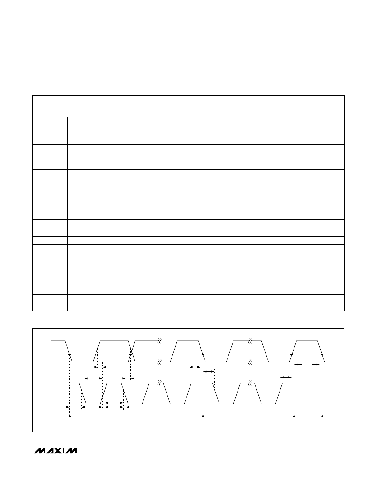
Serial Interface
The MAX520/MAX521 use a simple 2-wire serial interface
requiring only two I/O lines (2-wire bus) of a standard
microprocessor (µP) port. Figure 1 shows the timing dia-
gram for signals on the 2-wire bus. Figure 2 shows the
typical application of the MAX520/MAX521. The 2-wire
bus can have several devices (in addition to the
MAX520/MAX521) attached. The two bus lines (SDA and
SCL) must be high when the bus is not in use. When in
use, the port bits are toggled to generate the appropriate
signals for SDA and SCL. External pull-up resistors are
not required on these lines. The MAX520/MAX521 can
be used in applications where pull-up resistors are
required (such as in I
2
C systems) to maintain compatibil-
ity with the existing circuitry.
The MAX520/MAX521 are receive-only devices and
must be controlled by a bus master device. They oper-
ate at SCL rates up to 400kHz. A master device sends
information to the devices by transmitting their address
over the bus and then transmitting the desired informa-
tion. Each transmission consists of a START condition,
the MAX520/MAX521’s programmable slave-address,
one or more command-byte/output-byte pairs (or a
command byte alone, if it is the last byte in the trans-
mission), and finally, a STOP condition (Figure 3).
The address byte and pairs of command and output
bytes are transmitted between the START and STOP con-
ditions. The SDA state is allowed to change only while
SCL is low. SDA’s state is sampled, and therefore must
remain stable while SCL is high. The only exceptions to
this are the START and STOP conditions. Data is transmit-
ted in 8-bit bytes. Nine clock cycles are required to trans-
fer the data bits to the MAX520/MAX521. Set SDA low
during the 9th clock cycle as the MAX520/MAX521 pull
SDA low during this time. R
C
(Figure 2) limits the current
that flows during this time if SDA stays high for short peri-
ods of time.
MAX520
SDA
R
C
1k
SCL
µ
C
REF0
SDA
SCL
AD1
AD0
+1V
QUAD
DAC
REF1
+4V
REF2
+5V
OFFSET ADJUSTMENT
REF3
OUT0
OFFSET ADJUSTMENT
GAIN ADJUSTMENT
GAIN ADJUSTMENT
OUT1
OUT2
OUT3
.
.
.
.
AD2
REF0
SDA
SCL
AD1
AD0
OCTAL
DAC
+5V
BRIGHTNESS ADJUSTMENT
REF4
OUT0
CONTRAST ADJUSTMENT
OUT1
THRESHOLD
ADJUSTMENTS
OUT2
.
.
.
OUT6
OUT7
+5V
+5V
+12V
MOTOR
MAX521
Figure 2. Typical Application Circuit
START CONDITION
STOP CONDITION
OUTPUT BYTE
COMMAND BYTE
SLAVE ADDRESS BYTE
SCL
SDA
MSB
MSB
MSB
LSB
LSB
LSB
ACK
ACK
ACK
Figure 3. A Complete Serial Transmission
MAX520/MAX521
Quad/Octal, 2-Wire Serial 8-Bit DACs
with Rail-to-Rail Outputs
______________________________________________________________________________________
11
START and STOP Conditions
When the bus is not in use, both SCL and SDA must be
high. A bus master signals the beginning of a transmis-
sion with a START condition by transitioning SDA from
high to low while SCL is high (Figure 4). When the mas-
ter has finished communicating with the slave, it issues
a STOP condition by transitioning SDA from low to high
while SCL is high. The bus is then free for another
transmission.
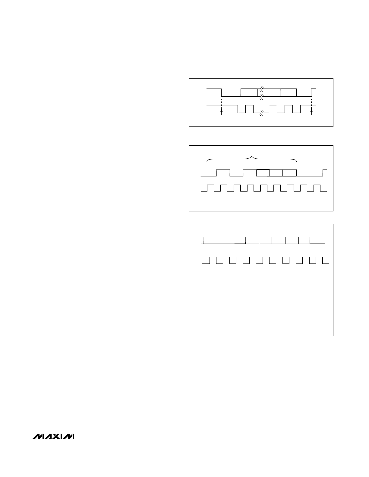
Slave Address
The MAX520/MAX521 each have a 7-bit-long slave
address (Figure 5). The first four bits (MSBs) of the slave
address have been factory programmed and are always
0101. In addition, the MAX521 has the next bit factory
programmed to 0. The logic state of the address input
pins (AD0, AD1, and AD2 of the MAX520; AD0 and AD1
of the MAX521) determine the least significant bits of the
7-bit slave address. These input pins may be connected
to V
DD
or DGND, or they may be actively driven by TTL
or CMOS logic levels. There are four possible slave
addresses for the MAX521, and therefore a maximum of
four such devices may be on the bus at one time. The
MAX520 has eight possible slave addresses. The eighth
bit (LSB) in the slave address byte should be low when
writing to the MAX520/MAX521.
The MAX520/MAX521 monitor the bus continuously,
waiting for a START condition followed by its slave
address. When a device recognizes its slave address, it
is ready to accept data.
Command Byte and Output Byte
A command byte follows the slave address. Figure 6
shows the format for the command byte. A command
byte is usually followed by an output byte unless it is
the last byte in the transmission. If it is the last byte, all
bits except PD and RST are ignored. If an output byte
follows the command byte, A0–A2 of the command
byte indicate the digital address of the DAC whose
input data latch receives the digital output data. The
data is transferred to the DAC’s output latch during the
STOP condition following the transmission. This allows
all DACs to be updated and the new outputs to appear
simultaneously (Figure 7).
Setting the PD bit high powers down the MAX520/
MAX521 following a STOP condition (Figure 8a). If a
command byte with PD set high is followed by an out-
put byte, the addressed DAC’s input latch will be
updated and the data will be transferred to the DAC’s
output latch following the STOP condition (Figure 8b). If
the transmission’s last command byte has PD high, the
voltage outputs will not reflect the newly entered data
because the DAC will enter power-down mode when
the STOP condition is detected. When in power-down,
the MAX521’s DAC outputs float, and the MAX520’s
unbuffered outputs look like a 16k
Ω
resistor to AGND.
In this mode, the supply current is a maximum of 20µA.
A command byte with the PD bit low returns the
MAX520/MAX521 to normal operation following a STOP
condition, and the voltage outputs reflect the current
output-latch contents (Figures 9a and 9b). Because
each subsequent command byte overwrites the previ-
ous PD bit, only the last command byte of a transmis-
sion affects the power-down state.
SCL
SDA
SLAVE ADDRESS BITS AD2, AD1, AND AD0 CORRESPOND TO THE LOGIC STATE
OF THE ADDRESS INPUT PINS AD2, AD1, AND AD0.
0
0
1
0 or AD2
1
0
AD1
AD0
LSB
ACK
SLAVE ADDRESS
Figure 5. Address Byte
LSB
MSB
SDA
SCL
R2
R1
R0
RST
PD
A2
A1
A0
ACK
R2, R1, R0: RESERVED BITS. SET TO 0.
RST: RESET BIT, SET TO 1 TO RESET ALL DAC REGISTERS.
PD: POWER-DOWN BIT. SET TO 1 TO PLACE THE DEVICE IN THE 4µA
SHUTDOWN MODE. SET TO 0 TO RETURN TO THE NORMAL
OPERATIONAL STATE.
A2, A1, A0: ADDRESS BITS. DIGITAL ADDRESS FOR DAC0 TO DAC7. DETERMINES
WHICH DAC'S INPUT LATCH RECEIVES THE 8 BITS OF DATA IN
THE NEXT BYTE. A2 IS IGNORED BY THE MAX520.
ACK: ACKNOWLEDGE BIT. THE MAX520/MAX521 PULL SDA LOW DURING THE
9TH CLOCK PULSE.
Figure 6. Command Byte
SCL
SDA
START CONDITION
STOP CONDITION
Figure 4. All communications begin with a START condition and
end with a STOP condition, both generated by a bus master.
MAX520/MAX521
Quad/Octal, 2-Wire Serial 8-Bit DACs
with Rail-to-Rail Outputs
12
______________________________________________________________________________________
( )
( )
SDA
SDA
0
START
CONDITION
ADDRESS BYTE
ACK
ACK
1
0
1
AD1 AD0 0
0
0
0
0
0
0
0
0
0
0
1
1
1
1
1
1
1
1
0 0
1
0
0
0
0
0
0
0
0
0
0
0
0
0
0
0
1
0
0
0
0
0
0
0
0
0
1
1
1
1
1
1
1
1
1
STOP
CONDITION
OUTPUT BYTE
(FULL SCALE)
COMMAND BYTE
(ADDRESSING DAC0)
ACK
OUTPUT BYTE
(FULL SCALE)
ACK
COMMAND BYTE
(ADDRESSING DAC2)
ACK
OUTPUT BYTE
(HALF SCALE)
ACK
COMMAND BYTE
(ADDRESSING DAC1)
ACK
DAC OUTPUTS CHANGE HERE:
DACS 0 AND 1 GO TO FULL SCALE,
DAC 2 GOES TO HALF SCALE.
DAC0 INPUT LATCH
SET TO FULL SCALE
( )
( )
DAC2 INPUT LATCH
SET TO HALF SCALE
DAC1 INPUT LATCH
SET TO FULL SCALE
0 OR AD2
Figure 7. Setting DAC Outputs
SDA
0
START
CONDITION
ADDRESS BYTE
ACK
1
0
1
AD1 AD0 0
0
0
0 0
0
0
1
(PD)
(PD)
STOP
CONDITION
COMMAND BYTE
ACK
DEVICE ENTERS
POWER-DOWN STATE
( )
SDA
0
START
CONDITION
ADDRESS BYTE
ACK
1
0
1
AD1 AD0 0
0
0
0
0
0
0
0
1
0
0
0
1
1
1
1
1
1
1
1
STOP
CONDITION
COMMAND BYTE
(ADDRESSING DAC0)
ACK
OUTPUT BYTE
(FULL SCALE)
ACK
(a)
(b)
DEVICE ENTERS POWER-DOWN STATE.
DAC 0 OUTPUT LATCH SET TO FULL SCALE.
NOTE: X = DON'T CARE
DAC 0 INPUT LATCH
SET TO FULL SCALE
X X X
( )
( )
0 OR AD2
0 OR AD2
Figure 8. Entering the Power-Down State
( )
SDA
0
START
CONDITION
ADDRESS BYTE
ACK
1
0
1
AD1 AD0 0
0
0
0 0
0
0
0
(PD)
(PD)
STOP
CONDITION
COMMAND BYTE
ACK
DEVICE RETURNS TO
NORMAL OPERATION
( )
DAC3 OUTPUT
LATCH SET TO 0
SDA
0
START
CONDITION
ADDRESS BYTE
ACK
1
0
1
AD1 AD0 0
0
0
0
0
0
0
0
1
1
0
0
0
0
0
0
0
0
0
0
STOP
CONDITION
COMMAND BYTE
(ADDRESSING DAC3)
ACK
OUTPUT BYTE
(SET TO 0)
ACK
(a)
(b)
DEVICE RETURNS TO NORMAL OPERATION.
DAC 3 SET TO 0.
NOTE: X = DON'T CARE
X X X
( )
0 OR AD2
0 OR AD2
Figure 9. Returning to Normal Operation from Power-Down
MAX520/MAX521
Quad/Octal, 2-Wire Serial 8-Bit DACs
with Rail-to-Rail Outputs
______________________________________________________________________________________
13
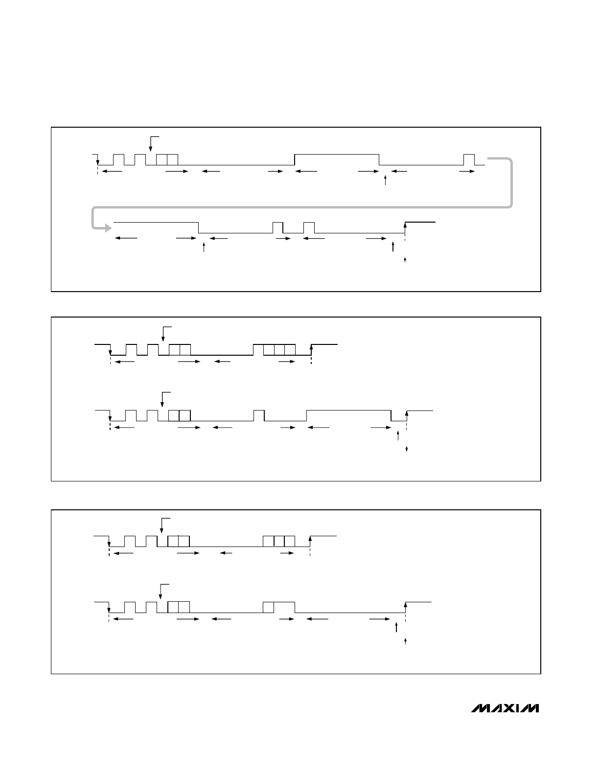
Setting the RST bit high clears all DAC input latches.
The DAC outputs remain unchanged until a STOP con-
dition is detected (Figure 10a). If a reset is issued, the
following output byte is ignored. Subsequent pairs of
command/output bytes overwrite the input latches
(Figure 10b).
All changes made during a transmission affect the
MAX520/MAX521’s outputs only when the transmission
ends and a STOP has been recognized. The R0, R1,
and R2 bits are reserved bits that must be set to zero.
I
2
C Compatibility
The MAX520/MAX521 are fully compatible with existing
I
2
C systems. SCL and SDA are high-impedance inputs;
SDA has an open drain which pulls the data line low
during the 9th clock pulse. Figure 11 shows a typical
I
2
C application.
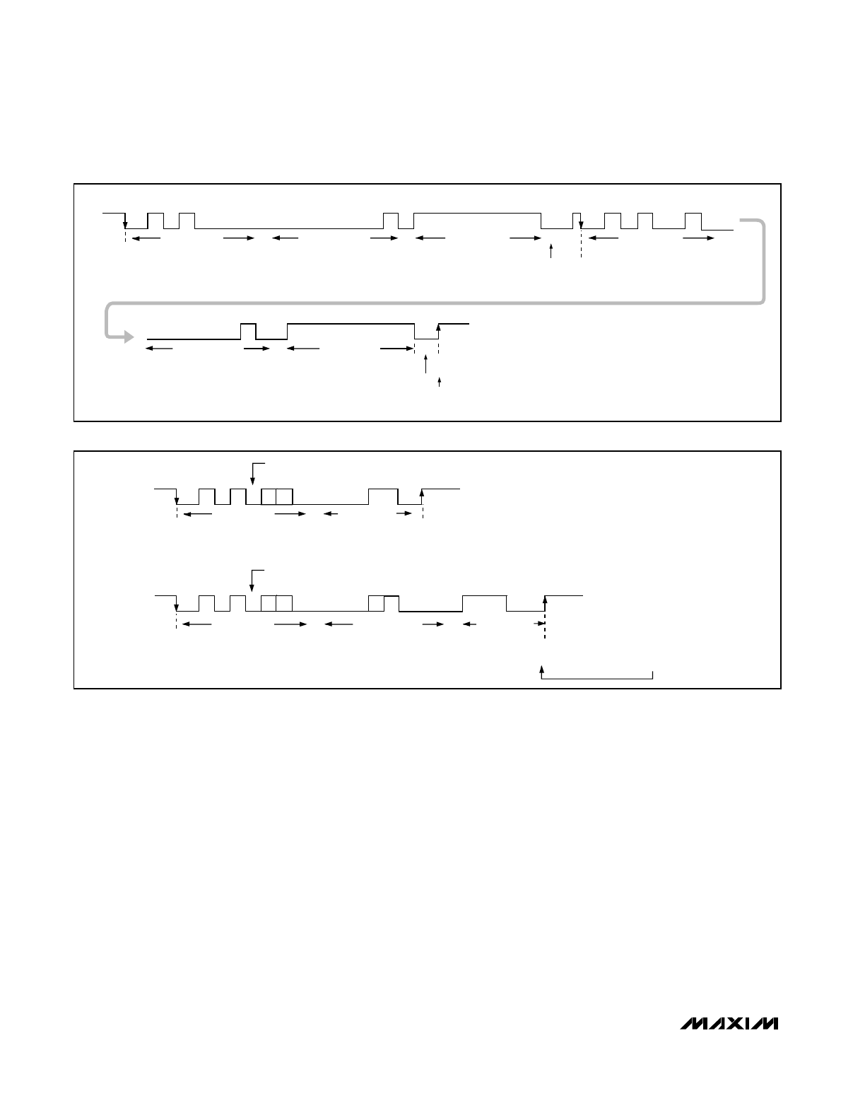
Additional START Conditions
It is possible to interrupt a transmission to a MAX520/
MAX521 with a new START (repeated start) condition
(perhaps addressing another device), which leaves the
input latches with data that has not been transferred to
the output latches (Figure 12). Only the currently
addressed device will recognize a STOP condition and
transfer data to its output latches. If the device is left
with data in its input latches, the data can be trans-
ferred to the output latches the next time the device is
addressed, as long as it receives at least one com-
mand byte and a STOP condition.
( )
( )
( )
SDA
0
START
CONDITION
ADDRESS BYTE
ACK
1
0
1
AD1 AD0 0
0
0 0
0
1
0
0
(RST)
(RST)
STOP
CONDITION
COMMAND BYTE
ACK
ALL OUTPUTS
SET TO 0
( )
ALL INPUT LATCHES
SET TO 0
ALL INPUT LATCHES
SET TO 0
SDA
0
START
CONDITION
ADDRESS BYTE
ACK
1
0
1
AD1 AD0 0
0
0
0
0
1
0
0
0
STOP
CONDITION
COMMAND BYTE
ACK
"DUMMY"
OUTPUT BYTE
ACK
(a)
(b)
ALL DAC OUTPUTS SET TO 0 UNLESS
CHANGED BY ADDITIONAL COMMAND
BYTE/OUTPUT BYTE PAIRS
NOTE: X = DON'T CARE
ADDITIONAL
COMMAND BYTE/
OUTPUT BYTE PAIRS
X X X
X X X
X X X X X X X X
0 OR AD2
0 OR AD2
Figure 10. Resetting DAC Outputs
MAX520
SDA SCL
µ
C
SDA
SCL
E
2
PROM
XICOR
X24C04
SDA
SCL
AD1
AD2
AD0
QUAD
DAC
SDA
SCL
AD1
AD0
OCTAL
DAC
+5V
MAX521
Figure 11. Typical I
2
C Application Circuit
MAX520/MAX521
Quad/Octal, 2-Wire Serial 8-Bit DACs
with Rail-to-Rail Outputs
14
______________________________________________________________________________________
Early Stop Conditions
The addressed device recognizes a STOP condition at
any point in a transmission. If the STOP occurs during a
command byte, all previous uninterrupted command
and output byte pairs are accepted, the interrupted
command byte is ignored, and the transmission ends
(Figure 13a). If the STOP occurs during an output byte,
all previous uninterrupted command and output byte
pairs are accepted, the final command byte’s PD and
RST bits are accepted, the interrupted output byte is
ignored, and the transmission ends (Figure 13b).
Analog Section
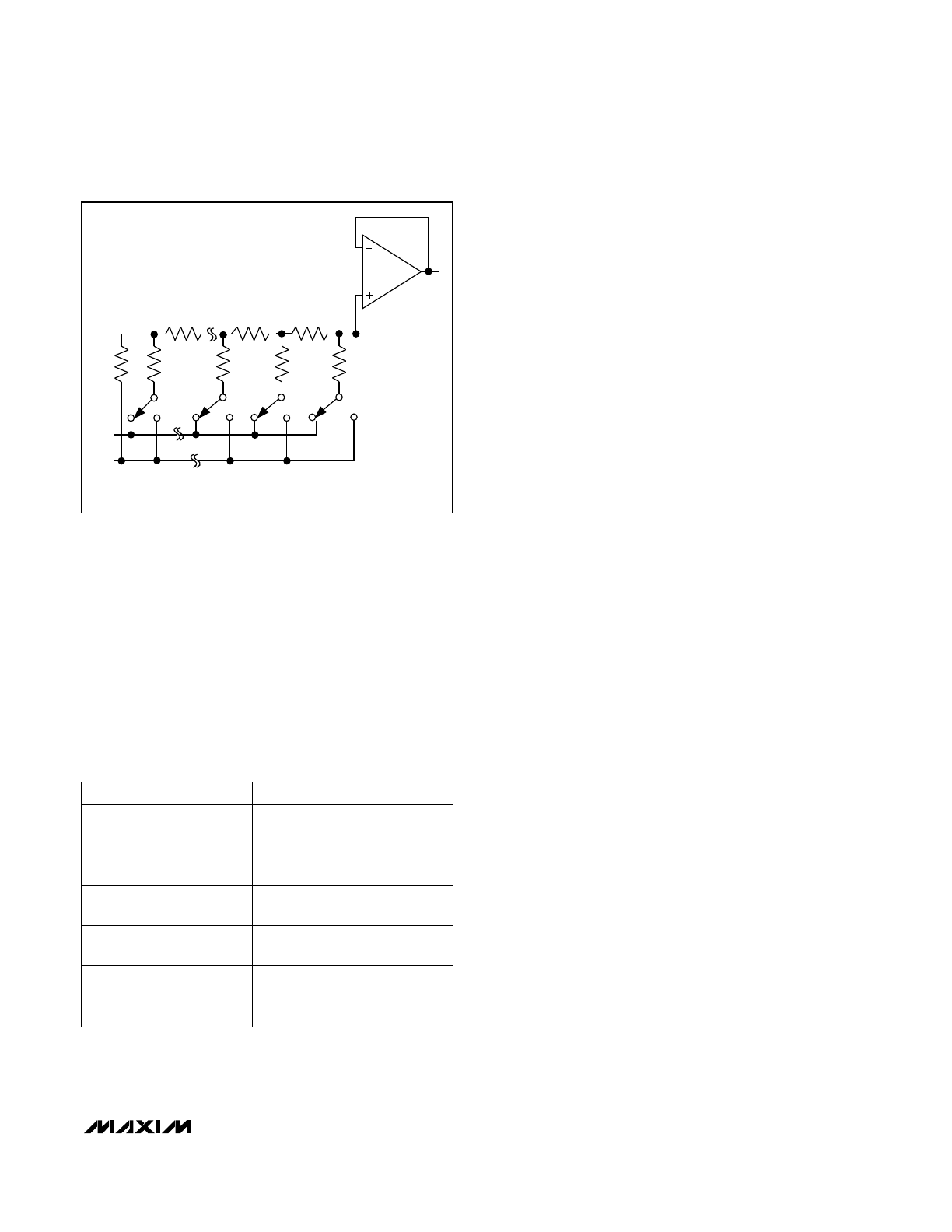
DAC Operation
The MAX520 contains four matched voltage-output
DACs, and the MAX521 contains eight. The DACs are
inverted R-2R ladder networks that convert 8-bit digital
words into equivalent analog output voltages in propor-
tion to the applied reference voltages. For both
devices, DAC0–DAC3 each have separate reference
inputs, while the MAX521’s DAC4–DAC7 all share a
common reference input. Figure 14 shows a simplified
diagram of one DAC.
Reference Inputs
The MAX520/MAX521 can be used for multiplying appli-
cations. The reference accepts a 0V to V
DD
voltage,
both DC and AC signals. The voltage at each REF input
sets the full-scale output voltage for its respective
DAC(s). The reference voltage must be positive. The
DAC’s input impedance is code dependent, with the
lowest value occurring when the input code is 55 hex or
0101 0101, and the maximum value occurring when the
input code is 00 hex. Since the REF input resistance
( )
( )
( )
SDA
0
START
CONDITION
ADDRESS BYTE
(DEVICE 0)
ACK
1
0
1
0
0
0
0
0
0
0
0
0
0
0
0
0
0
1
0
1
0
1
0
0
1
0
0
1
REPEATED START
CONDITION
STOP
CONDITION
COMMAND BYTE
ADDRESSING DAC1
COMMAND BYTE
(ADDRESSING DAC2)
ACK
OUTPUT BYTE
(FULL SCALE)
ACK
ADDRESS BYTE
(DEVICE 1)
ACK
DEVICE 0's
DAC1 INPUT LATCH
SET TO FULL SCALE
DEVICE 1's
DAC2 INPUT LATCH
SET TO FULL SCALE
SDA
ACK
ACK
OUTPUT BYTE
(FULL SCALE)
ONLY DEVICE 1's DAC2 OUTPUT LATCH SET TO FULL
SCALE. DEVICE 0's OUTPUT LATCHES UNCHANGED.
1
1
1
1
1
1
1
0
0
0
0
0
0
0
0
0
1
1
1
1
1
1
1
1
1
Figure 12. Repeated START Conditions
( )
SDA
0
0
START
CONDITION
ADDRESS BYTE
ACK
1
1
AD1 AD0 0
0
0 0
0
0
1
1
(RST) (PD)
(PD)
EARLY
STOP CONDITION
INTERRUPTED
COMMAND BYTE
MAX520/MAX521's STATES
REMAIN UNCHANGED
( )
SDA
0
START
CONDITION
ADDRESS BYTE
ACK
1
0
1
AD1 AD0 0
0
0
0
0
0
0
0
0
1
1
1
0
0
RST 1
COMMAND BYTE
(POWER DOWN)
ACK
INTERRUPTED
OUTPUT BYTE
(a)
(b)
MAX520/MAX521 POWER DOWN;
INPUT LATCHES UNCHANGED IF
RST = 0, DAC OUTPUTS RESET IF
RST = 1.
EARLY
STOP CONDITION
0 OR AD2
0 OR AD2
Figure 13. Early STOP Conditions
MAX520/MAX521
Quad/Octal, 2-Wire Serial 8-Bit DACs
with Rail-to-Rail Outputs
______________________________________________________________________________________
15
(R
IN
) is code dependent, it must be driven by a circuit
with low output impedance (no more than R
IN
÷ 2000) to
maintain output linearity. The REF input capacitance is
also code dependent, with the maximum value occur-
ring at code FF hex (typically 30pF for the MAX520/
MAX521’s REF0–REF3, and 120pF for the MAX521’s
REF4). The output voltage for any DAC can be repre-
sented by a digitally programmable voltage source as:
V
OUT
= (N x V
REF
) / 256, where N is the numerical value
of the DAC’s binary input code. Table 1 shows the
unipolar code.
MAX520 Unbuffered DAC Outputs
The unbuffered DAC outputs (OUT0–OUT3) connect
directly to the internal 16k
Ω
R-2R network. The outputs
swing from 0V to V
DD
.
The MAX520 has no output buffer amplifiers, giving it
very low supply current. The output-offset voltage is
lower without the output buffer, and the output can also
slew and settle faster if capacitive loading is minimized.
Resistive loading should be very light for highest accu-
racy. Any output loading generates some gain error,
increasing full-scale error. The R-2R ladder’s output
resistance is 16k
Ω
, so a 1µA output current creates a
16mV error. Linearity is not affected because the ladder
output resistance does not change with DAC code.
Ladder-resistance changes with temperature are also
very small.
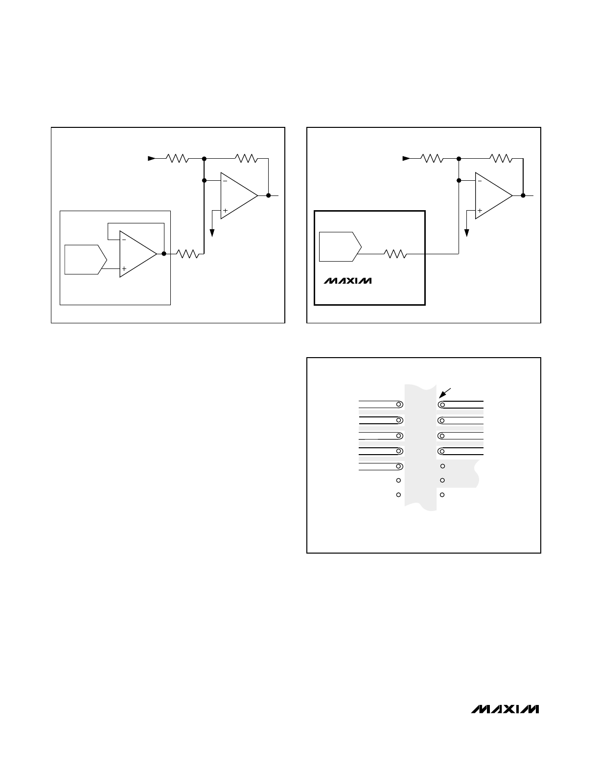
DACs are often used in trimming applications to
replace hardware potentiometers. Figure 15a shows a
typical application, which requires a buffered output so
that a precise current can be injected into the summing
node through precision resistor R
T
. For this application,
the MAX520A features a precise ±1% (T
A
= +25°C,
±2.5% over temperature) factory-trimmed output resis-
tance. Because the MAX520A’s output resistance is
precisely trimmed, there is no need for an internal
buffer or external precision resistor (Figure 15b). For
applications where the output resistance value is not
critical, use the MAX520B.
All DACs exhibit output glitches during code transitions.
An output filter is sometimes used to reduce these
glitches in sensitive applications. The MAX520 simpli-
fies output filtering because its internal resistive ladder
network serves as the “R” in an RC filter. Simply con-
nect a small capacitor from the DAC output to ground.
See the
Typical Operating Characteristics for oscillo-
scope photos of the worst-case 1LSB step change both
without and with 25pF of capacitance on the MAX520’s
output.
MAX521 Output Buffer Amplifiers
The MAX521 voltage outputs (OUT0–OUT7) are inter-
nally buffered precision unity-gain followers that slew
up to 1V/µs. The outputs can swing from 0V to V
DD
.
With a 0V to 4V (or 4V to 0V) output transition, the
amplifier outputs typically settle to 1/2LSB in 6µs when
loaded with 10k
Ω
in parallel with 100pF. The buffer
amplifiers are stable with any combination of resistive
loads
≥
2k
Ω
and capacitive loads
≤
300pF.
2R
R
R
R
2R
2R
2R
2R
2R
D0
D5
D6
D7
REF_
AGND
SHOWN FOR ALL 1s ON DAC
OUT_
(MAX521)
OUT_
(MAX520)
Figure 14. DAC Simplified Circuit Diagram
Table 1. Unipolar Code Table
0V
00000000
1
+ V
REF
(
———
)
256
00000001
127
+ V
REF
(
———
)
256
01111111
128 V
REF
+ V
REF
(
———
)
= ——
256 2
10000000
129
+ V
REF
(
———
)
256
10000001
255
+ V
REF
(
———
)
256
11111111
ANALOG OUTPUT
DAC CONTENTS
MAX520/MAX521
Quad/Octal, 2-Wire Serial 8-Bit DACs
with Rail-to-Rail Outputs
16
______________________________________________________________________________________
__________Applications Information
Shutdown Mode
In shutdown mode, the MAX520/MAX521 reference
inputs are disconnected from the R-2R ladder inputs,
which saves power when the reference is not powered
down. In addition, the MAX521’s output buffers are dis-
abled, greatly reducing the supply current. The
MAX520’s operating supply current does not change in
shutdown mode. The
Command Byte and Output Byte
section describes how to enter and exit shutdown
mode.
Power-Supply Bypassing and
Ground Management
Bypass V
DD
with a 0.1µF capacitor, located as close to
V
DD
and DGND as possible. The analog ground
(AGND) and digital ground (DGND) pins should be
connected in a “star” configuration to the highest quali-
ty ground available, which should be located as close
to the MAX521 as possible.
Careful PC board layout minimizes crosstalk among
DAC outputs, reference inputs, and digital inputs.
Figure 16 shows the suggested PC board layout to mini-
mize crosstalk.
OUT2
OUT3
REF2
REF3
OUT1
PIN1
OUT0
REF1
REF0
SYSTEM GND
Figure 16. PC Board Layout for Minimizing Crosstalk (MAX521
bottom view, DIP package)
(1%)
R
T
DAC
R
F
R
IN
Figure 15a. Typical Trimming Circuit
(1%)
16k
Ω
DAC
R
F
R
IN
MAX520A
Figure 15b. MAX520A Trimming Circuit
___________________________________________________Pin Configurations (continued)
20
19
18
17
16
15
14
13
1
2
3
4
5
6
7
8
OUT2
OUT3
REF2
N.C.
N.C.
REF1
OUT0
OUT1
TOP VIEW
REF3
V
DD
N.C.
AD2
DGND
N.C.
AGND
REF0
12
11
9
10
AD1
AD0
SDA
SCL
SSOP
MAX520
20
19
18
17
16
15
14
13
1
2
3
4
5
6
7
8
OUT2
OUT3
REF2
REF3
REF0
REF1
OUT0
OUT1
REF4
V
DD
AD1
AD0
SDA
SCL
AGND
DGND
12
11
9
10
OUT7
OUT6
OUT5
OUT4
DIP
MAX521
24
23
22
21
20
19
18
17
1
2
3
4
5
6
7
8
OUT2
OUT3
REF2
REF3
REF0
REF1
OUT0
OUT1
N.C.
REF4
V
DD
AD1
SCL
N.C.
AGND
DGND
16
15
14
13
9
10
11
12
N.C.
AD0
OUT7
OUT6
OUT5
OUT4
SDA
N.C.
SO/SSOP
MAX521
________________________________________________Functional Diagrams (continued)
MAX520/MAX521
Quad/Octal, 2-Wire Serial 8-Bit DACs
with Rail-to-Rail Outputs
______________________________________________________________________________________
17
INPUT
LATCH 0
8-BIT
SHIFT REGISTER
8
SCL
REF0
REF1
SDA
REF2
OUTPUT
LATCH 0
DAC0
OUT0
1
MAX521
INPUT
LATCH 1
8
OUTPUT
LATCH 1
DAC1
OUT1
ADDRESS
COMPARATOR
1
START/STOP
DETECTOR
DECODE
INPUT
LATCH 2
8
OUTPUT
LATCH 2
DAC2
OUT2
1
INPUT
LATCH 3
8
OUTPUT
LATCH 3
DAC3
OUT3
8
8
INPUT
LATCH 4
8
OUTPUT
LATCH 4
DAC4
OUT4
INPUT
LATCH 5
8
OUTPUT
LATCH 5
DAC5
OUT5
INPUT
LATCH 6
8
OUTPUT
LATCH 6
DAC6
OUT6
INPUT
LATCH 7
8
OUTPUT
LATCH 7
DAC7
OUT7
REF4
REF3
AD1
AD0
1
1
1
1
1
MAX520/MAX521
Quad/Octal, 2-Wire Serial 8-Bit DACs
with Rail-to-Rail Outputs
18
______________________________________________________________________________________
TRANSISTOR COUNT: 4518
SUBSTRATE CONNECTED TO V
DD
_________________Chip Topographies
SCLK
SDATA
AD0
AD1
AD2
0.121"
(3.073mm)
0.098"
(2.489mm)
V
DD
REF3
REF1
OUT0
OUT1
OUT2
OUT3
REF2
DGND
AGND
REF0
SDA
SCL
AGND
AGND
DGND
REF0
OUT7
0.212"
(5.385mm)
0.125"
(3.175mm)
OUT4 OUT5 OUT6
REF3
AD0
AD1
V
DD
REF4
REF2
OUT2
OUT3
OUT1
OUT0
REF1
* Dice are specified at T
A
= +25°C, DC parameters only.
†
MAX520 “A” grade parts include a 1%-accurate, factory-trimmed
output resistance.
PART
†
TEMP. RANGE
PIN-PACKAGE
TUE
(LSB)
MAX521
ACPP
0°C to +70°C
20 Plastic DIP
1
MAX521BCPP
MAX521ACWG
MAX521BCWG
0°C to +70°C
0°C to +70°C
0°C to +70°C
20 Plastic DIP
24 Wide SO
24 Wide SO
2
1
2
MAX521ACAG
MAX521BCAG
MAX521BC/D
0°C to +70°C
0°C to +70°C
0°C to +70°C
24 SSOP
24 SSOP
Dice*
1
2
2
__Ordering Information (continued)
MAX521AEPP
-40°C to +85°C
20 Plastic DIP
1
MAX521BEPP
MAX521AEWG
MAX521BEWG
-40°C to +85°C
-40°C to +85°C
-40°C to +85°C
20 Plastic DIP
24 Wide SO
24 Wide SO
2
1
2
MAX521AEAG
MAX521BEAG
MAX521BMJP
-55°C to +125°C
-40°C to +85°C
-40°C to +85°C
24 SSOP
24 SSOP
20 CERDIP
1
2
2
MAX520
MAX521
MAX520AEPE
-40°C to +85°C
16 Plastic DIP
1
MAX520BEPE
MAX520AEWE
MAX520BEWE
-40°C to +85°C
-40°C to +85°C
-40°C to +85°C
16 Plastic DIP
16 Wide SO
16 Wide SO
1
1
1
MAX520AEAP
-40°C to +85°C
20 SSOP
1
MAX520BEAP
MAX520AMJE
MAX520BMJE
-55°C to +125°C
-55°C to +125°C
-40°C to +85°C
20 SSOP
16 CERDIP
16 CERDIP
1
1
1
MAX520AC/D
0°C to +70°C
Dice*
1
MAX520BCAP
0°C to +70°C
20 SSOP
1
MAX520ACAP
0°C to +70°C
20 SSOP
1
MAX520BC/D
0°C to +70°C
Dice*
1
MAX520/MAX521
Quad/Octal, 2-Wire Serial 8-Bit DACs
with Rail-to-Rail Outputs
______________________________________________________________________________________
19
________________________________________________________Package Information
DIM
A
A1
A2
A3
B
B1
C
D1
E
E1
e
eA
eB
L
MIN
–
0.015
0.125
0.055
0.016
0.045
0.008
0.005
0.300
0.240
0.100
0.300
–
0.115
MAX
0.200
–
0.175
0.080
0.022
0.065
0.012
0.080
0.325
0.310
–
–
0.400
0.150
MIN
–
0.38
3.18
1.40
0.41
1.14
0.20
0.13
7.62
6.10
2.54
7.62
–
2.92
MAX
5.08
–
4.45
2.03
0.56
1.65
0.30
2.03
8.26
7.87
–
–
10.16
3.81
INCHES
MILLIMETERS
Plastic DIP
PLASTIC
DUAL-IN-LINE
PACKAGE
(0.300 in.)
DIM
D
D
D
D
D
D
PKG.
P
P
P
P
P
N
MIN
0.348
0.735
0.745
0.885
1.015
1.14
MAX
0.390
0.765
0.765
0.915
1.045
1.265
MIN
8.84
18.67
18.92
22.48
25.78
28.96
MAX
9.91
19.43
19.43
23.24
26.54
32.13
INCHES
MILLIMETERS
PINS
8
14
16
18
20
24
C
A
A2
E1
D
E
eA
eB
A3
B1
B
0° - 15°
A1
L
D1
e
21-0043A
DIM
A
A1
B
C
E
e
H
L
MIN
0.093
0.004
0.014
0.009
0.291
0.394
0.016
MAX
0.104
0.012
0.019
0.013
0.299
0.419
0.050
MIN
2.35
0.10
0.35
0.23
7.40
10.00
0.40
MAX
2.65
0.30
0.49
0.32
7.60
10.65
1.27
INCHES
MILLIMETERS
21-0042A
Wide SO
SMALL-OUTLINE
PACKAGE
(0.300 in.)
DIM
D
D
D
D
D
MIN
0.398
0.447
0.496
0.598
0.697
MAX
0.413
0.463
0.512
0.614
0.713
MIN
10.10
11.35
12.60
15.20
17.70
MAX
10.50
11.75
13.00
15.60
18.10
INCHES
MILLIMETERS
PINS
16
18
20
24
28
1.27
0.050
L
H
E
D
e
A
A1
C
0°- 8°
0.101mm
0.004in.
B
Maxim cannot assume responsibility for use of any circuitry other than circuitry entirely embodied in a Maxim product. No circuit patent licenses are
implied. Maxim reserves the right to change the circuitry and specifications without notice at any time.
20
__________________Maxim Integrated Products, 120 San Gabriel Drive, Sunnyvale, CA 94086 (408) 737-7600
© 1996 Maxim Integrated Products
Printed USA
is a registered trademark of Maxim Integrated Products.
MAX520/MAX521
Quad/Octal, 2-Wire Serial 8-Bit DACs
with Rail-to-Rail Outputs
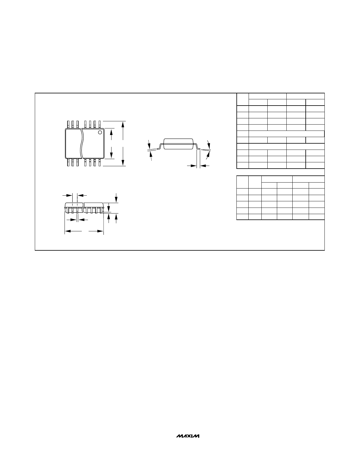
___________________________________________Package Information (continued)
L
DIM
A
A1
B
C
D
E
e
H
L
α
DIM
D
D
D
D
D
MIN
0.068
0.002
0.010
0.004
0.205
0.301
0.025
0˚
MIN
0.239
0.239
0.278
0.317
0.397
MAX
0.078
0.008
0.015
0.008
0.209
0.311
0.037
8˚
MAX
0.249
0.249
0.289
0.328
0.407
MIN
1.73
0.05
0.25
0.09
5.20
7.65
0.63
0˚
MIN
6.07
6.07
7.07
8.07
10.07
MAX
1.99
0.21
0.38
0.20
5.38
7.90
0.95
8˚
PINS
14
16
20
24
28
MAX
6.33
6.33
7.33
8.33
10.33
INCHES
INCHES
MILLIMETERS
MILLIMETERS
α
SSOP
SHRINK
SMALL-OUTLINE
PACKAGE
H
E
D
A
A1
C
B
0.65 BSC
0.0256 BSC
21-0056A
e
SEE VARIATIONS