
_______________General Description
The MAX512/MAX513 contain three 8-bit, voltage-output
digital-to-analog converters (DAC A, DAC B, and DAC C).
Output buffer amplifiers for DACs A and B provide voltage
outputs while reducing external component count. The
output buffer for DAC A can source or sink 5mA to within
0.5V of V
DD
or V
SS
. The buffer for DAC B can source or
sink 0.5mA to within 0.5V of V
DD
or V
SS
. DAC C is
unbuffered, providing a third voltage output with increased
accuracy. The MAX512 operates with a single
+5V ±10% supply, and the MAX513 operates with a
+2.7V to +3.6V supply. Both devices can also operate
with split supplies.
The 3-wire serial interface has a maximum operating fre-
quency of 5MHz and is compatible with SPI™, QSPI™,
and Microwire™. The serial input shift register is 16 bits
long and consists of 8 bits of DAC input data and 8 bits
for DAC selection and shutdown. DAC registers can be
loaded independently or in parallel at the positive edge
of
–
C
—
S
–
. A latched logic output is also available for auxil-
iary control.
Ultra-low power consumption and small packages
(14-pin DIP/SO) make the MAX512/MAX513 ideal for
portable and battery-powered applications. Supply cur-
rent is only 1mA, dropping to less than 1µA in shutdown.
Any of the three DACs can be independently shut down.
In shutdown mode, the DAC's R-2R ladder network is
disconnected from the reference input, minimizing sys-
tem power consumption.
________________________Applications
Digital Gain and Offset Adjustment
Programmable Attenuators
Programmable Current Sources
Programmable Voltage Sources
RF Digitally Adjustable Bias Circuits
VCO Tuning
____________________________Features
♦
Operate from a Single +5V (MAX512) or
+3V (MAX513) Supply, or from Bipolar Supplies
♦
Low Power Consumption
1mA Operating Current
<1µA Shutdown Current
♦
Unipolar or Bipolar Outputs
♦
5MHz, 3-Wire Serial Interface
♦
SPI, QSPI, and Microwire Compatible
♦
Two Buffered, Bipolar-Output DACs (DACs A/B)
♦
Independently Programmable Shutdown Mode
♦
Space-Saving 14-Pin SO/DIP Packages
♦
Pin and Software Reset
______________Ordering Information
Ordering Information continued at end of data sheet.
* Contact factory for dice specifications.
MAX512/MAX513
Low-Cost, Triple, 8-Bit Voltage-Output DACs
with Serial Interface
________________________________________________________________
Maxim Integrated Products
1
DAC
LATCH
A
DAC A
DAC
LATCH
B
DAC B
DAC
LATCH
C
LATCH
DAC C
SCLK
OUTA
OUTB
OUTC
LOUT
DIN
CS
REFAB
REFC
RESET
V
DD
V
SS
GND
16-BIT SHIFT REGISTER
CONTROL (8)
DATA (8)
MAX512
MAX513
1
2
4
5
6
7
8
9
10
11
12
14
3
________________Functional Diagram
1
2
3
4
14
13
12
11
LOUT
I.C.
REFAB
REFC
RESET
SCLK
CS
DIN
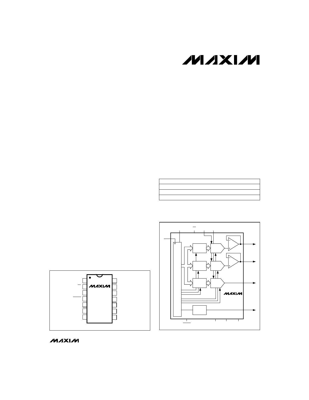
DIP/SO
TOP VIEW
MAX512
MAX513
5
6
7
10
9
8
OUTC
OUTB
OUTA
V
SS
GND
V
DD
__________________Pin Configuration
19-0252; Rev 2; 5/96
PART
TEMP. RANGE
PIN-PACKAGE
MAX512
CPD
0°C to +70°C
14 Plastic DIP
MAX512CSD
0°C to +70°C
14 SO
MAX512C/D
0°C to +70°C
Dice*
Microwire is a trademark of National Semiconductor Corp. SPI and QSPI are trademarks of Motorola Inc.
For free samples & the latest literature: http://www.maxim-ic.com, or phone 1-800-998-8800
LSB
MAX512/MAX513
Low-Cost, Triple, 8-Bit Voltage-Output DACs
with Serial Interface
2
_______________________________________________________________________________________
ABSOLUTE MAXIMUM RATINGS
ELECTRICAL CHARACTERISTICS
(V
DD
= +4.5V to +5.5V for MAX512, V
DD
= +2.7V to +3.6V for MAX513, V
SS
= GND = 0V, REFAB = REFC = V
DD
,
T
A
= T
MIN
to T
MAX
, unless otherwise noted. Typical values are at T
A
= +25°C.)
Note 1:
The outputs may be shorted to V
DD
, V
SS
, or GND if the package power dissipation is not exceeded. Typical short-circuit cur-
rent to GND is 50mA.
Stresses beyond those listed under “Absolute Maximum Ratings” may cause permanent damage to the device. These are stress ratings only, and functional
operation of the device at these or any other conditions beyond those indicated in the operational sections of the specifications is not implied. Exposure to
absolute maximum rating conditions for extended periods may affect device reliability.
V
DD
to GND ................................................................ -0.3V, +6V
V
SS
to GND ................................................................. -6V, +0.3V
V
DD
to V
SS
................................................................ -0.3V, +12V
Digital Inputs and Outputs to GND............... -0.3V, (V
DD
+ 0.3V)
REFAB ................................................ (V
SS
- 0.3V), (V
DD
+ 0.3V)
OUTA, OUTB (Note 1) ....................................................V
SS
, V
DD
OUTC.............................................................-0.3V, (V
DD
+ 0.3V)
REFC..............................................................-0.3V, (V
DD
+ 0.3V)
Continuous Power Dissipation (T
A
= +70°C)
Plastic DIP (derate 10.00mW/°C above +70°C) ............800mW
SO (derate 8.33mW/°C above +70°C) ...........................667mW
CERDIP (derate 9.09mW/°C above +70°C) ...................727mW
Operating Temperature Ranges
MAX51_C_ _ .........................................................0°C to +70°C
MAX51_E_ _.......................................................-40°C to +85°C
MAX51_MJD ....................................................-55°C to +125°C
Storage Temperature Range .............................-65°C to +165°C
Lead Temperature (soldering, 10sec) .............................+300°C
REFAB, REFC
REFC (Note 3)
REFAB (Note 3)
REFC
REFAB
MAX513, 2.7V
≤
V
DD
≤
3.6V,
REFAB = REFC = 2.4V
MAX512, 4.5V
≤
V
DD
≤
5.5V,
REFAB = REFC = 4.096V
DAC C
DAC A/B
CONDITIONS
M
Ω
2
Reference Input Resistance
(shutdown mode)
k
Ω
12
R
REF
Reference Input Resistance
8
pF
25
Reference Input Capacitance
V
GND
V
DD
Reference Input Voltage Range
V
SS
V
DD
%/%
0.01
PSRR
Power-Supply Rejection Ratio
Bits
8
N
Resolution
µV/°C
5
Zero-Code Temperature
Coefficient
100
UNITS
MIN
TYP
MAX
SYMBOL
PARAMETER
Guaranteed monotonic
LSB
±1
DNL
Differential Nonlinearity
0.015
DAC A/B (Note 2)
LSB
±1.5
INL
Integral Nonlinearity
(Note 2)
LSB
±1
TUE
Total Unadjusted Error
DAC C
±1
STATIC PERFORMANCE
REFERENCE INPUTS
MAX512/MAX513
Low-Cost, Triple, 8-Bit Voltage-Output DACs
with Serial Interface
_______________________________________________________________________________________
3
Note 2:
Digital code from 24 through 232 are due to swing limitations of output amplifiers on DAC A and DAC B. See
Typical
Operating Characteristics.
Note 3:
Reference input resistance is code dependent. The lowest input resistance occurs at code 55hex. Refer to the reference
input section in the
Detailed Description.
Note 4:
Guaranteed by design. Not production tested.
Note 5:
Input capacitance is code dependent. The highest capacitance occurs at code 00hex.
Note 6:
For single-supply mode, tie V
SS
to GND.
DAC A
(Notes 4, 5)
V
IN
= 0V or V
DD
I
SINK
≤
1.6mA
DAC B
DAC C
I
SOURCE
≤
1.6mA
CONDITIONS
V
0.4
V
OL
Output Low Voltage
V
V
DD
- 0.4
V
OH
Output High Voltage
µF
0.10
V
0
REF_
Output Voltage Range
pF
10
C
IN
Input Capacitance
µA
0.1
±10
I
IN
Input Current
V
(0.3)(V
DD
)
V
IL
Input Low Voltage
V
(0.7)(V
DD
)
V
IH
Input High Voltage
0.01
0
Capacitive Load
UNITS
MIN
TYP
MAX
SYMBOL
PARAMETER
ELECTRICAL CHARACTERISTICS (continued)
(V
DD
= +4.5V to +5.5V for MAX512, V
DD
= +2.7V to +3.6V for MAX513, V
SS
= GND = 0V, REFAB = REFC = V
DD
,
T
A
= T
MIN
to T
MAX
, unless otherwise noted. Typical values are at T
A
= +25°C.)
Voltage-Output Slew Rate
SR
C
L
= 0.1µF (DAC A), C
L
= 0.01µF (DAC B)
0.1
V/µs
70
Voltage-Output Settling Time
To ±
1
⁄
2
LSB
35
µs
Digital Feedthrough and Crosstalk
All 0s to all 1s
10
nV-s
Positive Supply Voltage Range
V
DD
MAX512
4.5
5.5
V
Shutdown Supply Current
0.1
µA
Negative Supply Current
I
SS
All inputs = 0V, V
SS
= -5.5V
-1.3
mA
C
L
= 0.1µF (DAC A)
C
L
= 0.01µF (DAC B)
C
L
= 0.1nF (DAC C)
70
DAC A
DAC B
DAC C
k
Ω
0.050
0.500
24
Output Resistance
MAX513
2.7
3.6
Negative Supply Voltage Range
(Note 6)
V
SS
MAX512
-5.5
-4.5
V
MAX513
-3.6
-2.7
Positive Supply Current
I
DD
All inputs = 0V
1.3
2.8
mA
0.9
2.5
DAC OUTPUTS
DYNAMIC PERFORMANCE
DIGITAL OUTPUT
POWER SUPPLIES
DIGITAL INPUTS
MAX512 (V
DD
= 5.5V)
MAX513 (V
DD
= 3.6V)
MAX512/MAX513
Low-Cost, Triple, 8-Bit Voltage Output DACs
with Serial Interface
4
_______________________________________________________________________________________
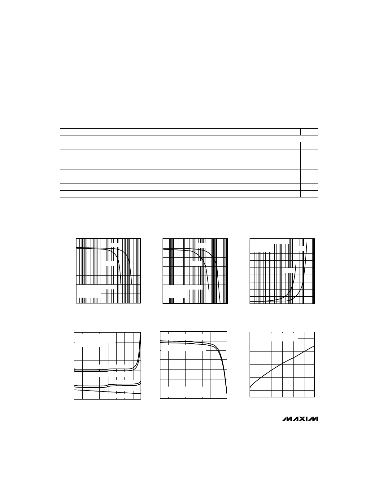
__________________________________________Typical Operating Characteristics
(T
A
= +25°C, unless otherwise noted.)
0.0001
0.1
100
0.01
10
0.001
1
OUTPUT VOLTAGE vs.
OUTPUT SOURCE CURRENT (V
DD
= 3V)
0.5
MAX512 TOC-01
OUTPUT SOURCE CURRENT (mA)
OUTPUT VOLTAGE (V)
1.5
2.5
3.5
0
1
2
3
V
DD
= 3V, V
SS
= GND = 0V
REFAB = V
DD
CODE = ALL 1s
DAC A
DAC B
-2
0
224
TOTAL UNADJUSTED ERROR
vs. DIGITAL CODE (Dual Supplies)
0
8
12
10
MAX512 TOC-04
DIGITAL CODE
TUE (LSB)
160
4
2
32
96
255
192
64
128
6
V
DD
= +3V, V
SS
= -3V
REFAB = V
SS
, REFC = V
DD
CODE = ALL 1s
DAC A LOADED WITH 5mA
DAC B LOADED WITH 0.5mA
DAC B NO LOAD
DAC A NO LOAD
DAC C NO LOAD
0.0001
0.1
100
0.01
10
0.001
1
OUTPUT VOLTAGE vs.
OUTPUT SOURCE CURRENT (V
DD
= 5V)
3.8
MAX512 TOC-02
OUTPUT SOURCE CURRENT (mA)
OUTPUT VOLTAGE (V) 4.2
4.6
5.0
5.2
4.0
4.4
4.8
V
DD
= 5V, V
SS
= GND = 0V
REFAB = V
DD
CODE = ALL 1s
DAC A
DAC B
0.0001
0.1
100
0.01
10
0.001
1
OUTPUT VOLTAGE vs.
OUTPUT SINK CURRENT
100
MAX512 TOC-03
OUTPUT SINK CURRENT (mA)
OUTPUT VOLTAGE (mV)
300
500
700
800
900
0
200
400
600
V
DD
= 3V, V
SS
= GND = 0V
REFAB = V
DD
CODE = ALL 1s
DAC A
DAC B
0
-35
0
192 224 255
TOTAL UNADJUSTED ERROR
vs. DIGITAL CODE (Single Supply)
-30
-10
-5
MAX512 TOC-05
DIGITAL CODE
TUE (LSB)
96
128
160
-20
-25
32
64
-15
V
DD
= 3V, V
SS
= GND = 0V
REFAB = 3V
DAC A LOADED WITH 5mA
DAC B LOADED WITH 0.5mA
1.2
0.5
2.5
4.5
5.0
5.5
POSITIVE SUPPLY CURRENT
vs. SUPPLY VOLTAGE
0.6
1.0
1.1
1.5
1.3
1.4
MAX512 TOC-06
V
DD
(V)
I
DD
(mA)
4.0
0.8
0.7
3.0
3.5
0.9
REFAB = REFC = V
DD
ALL LOGIC INPUTS GROUNDED
CONDITIONS
C
L
= 100pF
ns
200
t
CSPWH
–
C
—
S
–
Pulse Width High
ns
150
t
OD
Output Delay LOUT
ns
100
t
CL
SCLK Pulse Width Low
ns
100
t
CH
SCLK Pulse Width High
ns
50
t
DH
DIN to SCLK Rise Hold Time
ns
50
t
DS
DIN to SCLK Rise Setup Time
UNITS
MIN
TYP
MAX
SYMBOL
PARAMETER
ns
150
t
CSS
–
C
—
S
–
Fall to SCLK Rise Setup Time
ns
150
t
CSH
SCLK Rise to
–
C
—
S
–
Rise Setup Time
TIMING CHARACTERISTICS (Note 4)
(V
DD
= +4.5V to +5.5V for MAX512, V
DD
= +2.7V to +3.6V for MAX513, V
SS
= GND = 0V, T
A
= T
MIN
to T
MAX
, unless otherwise noted.)
SERIAL INTERFACE TIMING
Note 4:
Guaranteed by design. Not production tested.
MAX512/MAX513
Low-Cost, Triple, 8-Bit Voltage Output DACs
with Serial Interface
_______________________________________________________________________________________
5
-1.5
-5
2
4
SUPPLY CURRENT
vs. REFERENCE VOLTAGE
-1.0
1.0
1.5
MAX512 TOC-07
REFAB = REFC (V)
I
SUPPLY
(mA)
0
0
-0.5
-4
-2
3
1
-3
-1
0.5
I
DD
, V
DD
= 3V, V
SS
= -3V
I
SS
, V
DD
= 3V, V
SS
= -3V
I
SS
, V
DD
= 5V, V
SS
= -5V
I
DD
, V
DD
= 5V, V
SS
= -5V
REFC GROUNDED FOR REF_ < 0
CODE = ALL 1s
1.340
-60
80
120 140
POSITIVE SUPPLY CURRENT
vs. TEMPERATURE
1.345
1.365
1.370
MAX512 TOC-08
TEMPERATURE (°C)
I
DD
(mA)
40
1.355
1.350
-40
0
100
60
-20
20
1.360
V
DD
= +5V, V
SS
= GND = 0V
REFAB = REFC = V
DD
ALL LOGIC INPUTS = +5V
ALL DACs SET TO ALL 1s
0
0.5
-60
80
120 140
SHUTDOWN SUPPLY CURRENT
vs. TEMPERATURE
1.0
1.5
4.0
4.5
MAX512 TOC-09
TEMPERATURE (°C)
SHUTDOWN SUPPLY CURRENT (
µ
A)
40
3.0
2.5
2.0
-40
0
100
60
-20
20
3.5
V
DD
= +5V, V
SS
= GND = 0V
REFAB = REFC = V
DD
ALL LOGIC INPUTS = +5V
0.01
10
1
1000
0.1
100
REFERENCE FEEDTHROUGH
vs. FREQUENCY
-100
MAX512 TOC-10
FREQUENCY (kHz)
FEEDTHROUGH (dB)
-60
-20
-120
-80
-40
0
V
DD
= 3V, V
SS
= GND = 0V
REF_ FROM 0V TO 2.9V
NO LOAD
CODE = ALL 0s
DAC A, B
DAC C
0.001
1
1000
0.1
100
0.01
10
REFERENCE LARGE-SIGNAL
FREQUENCY RESPONSE
-20
MAX512 TOC-11
FREQUENCY (kHz)
RELATIVE OUTPUT (dB)
-10
0
-25
-15
-5
5
V
DD
= 3V, V
SS
= GND = 0V
REFAB, REFC
SINE WAVE 0V TO V
DD
100k
10k
1k
0.1k
1M
10M
REFERENCE SMALL-SIGNAL
FREQUENCY RESPONSE
-80
MAX512 TOC-12
FREQUENCY (Hz)
RELATIVE OUTPUT (dB)
-40
0
-60
-20
DAC C
DAC A
DAC B
V
DD
= 3V, V
SS
= GND = 0V
REFAB, REFC
SINE WAVE ±40mV
____________________________Typical Operating Characteristics (continued)
(T
A
= +25°C, unless otherwise noted.)
CLOCK FEEDTHROUGH (OUTA)
B
1
µ
s/div
A
A: SCLK, 333kHz, 0V TO 2.9V, 2V/div
B: OUTA, 2mV/div
V
SS
= 0V, CS = HIGH
CLOCK FEEDTHROUGH (OUTC)
B
1
µ
s/div
A
A: SCLK, 333kHz, 0V TO 2.9V, 2V/div
B: OUTC, 2mV/div
V
SS
= 0V, CS = HIGH
MAX512/MAX513
Low-Cost, Triple, 8-Bit Voltage Output DACs
with Serial Interface
6
_______________________________________________________________________________________
____________________________Typical Operating Characteristics (continued)
(T
A
= +25°C, unless otherwise noted.)
3.14V
LINE-TRANSIENT RESPONSE (OUTA)
2.86V
20
µ
s/div
A : V
DD,
100mV/div
B : OUTA, 500
µ
V/div
REFAB = 2.56V, NO LOAD, CODE = ALL 1s
A
B
LINE-TRANSIENT RESPONSE (OUTC)
3.14V
2.86V
20
µ
s/div
A : V
DD
, 100mV/div
REFC = 2.56V, NO LOAD, CODE = ALL 1s
B : OUTC, 2mV/div
A
B
MAX512/MAX513
Low-Cost, Triple, 8-Bit Voltage Output DACs
with Serial Interface
_______________________________________________________________________________________
7
____________________________Typical Operating Characteristics (continued)
(T
A
= +25°C, unless otherwise noted.)
A
POSITIVE SETTLING TIME (DAC A)
20
µ
s/div
V
DD
= 3V, V
SS
= 0V, REFAB = V
DD,
R
L
= 1k
Ω
, C
L
= 0.1
µ
F
ALL BITS OFF TO ALL BITS ON
B
A: CS, 2V/div
B: OUTA, 20mV/div
A
POSITIVE SETTLING TIME (DAC C)
10
µ
s/div
V
DD
= 3V, V
SS
= 0V, REFC = V
DD,
R
L
=
∞
, C
L
= 122pF
ALL BITS OFF TO ALL BITS ON
B
A: CS, 2V/div
B: OUTC, 20mV/div
A
POSITIVE SETTLING TIME (DAC B)
20
µ
s/div
V
DD
= 3V, V
SS
= 0V, REFAB = V
DD,
R
L
= 10k
Ω
, C
L
= 0.01
µ
F
ALL BITS OFF TO ALL BITS ON
B
A: CS, 2V/div
B: OUTB, 20mV/div
A
POSITIVE SETTLING TIME WITH DUAL SUPPLIES
10
µ
s/div
V
DD
= 5V, V
SS
= -5V, REFAB = 2.56V, R
L
= 1k
Ω
, C
L
= 0.1
µ
F
ALL BITS OFF TO ALL BITS ON
B
A: CS, 5V/div
B: OUTA, 10mV/div
MAX512/MAX513
Low-Cost, Triple, 8-Bit Voltage-Output DACs
with Serial Interface
8
_______________________________________________________________________________________
A
TIME EXITING SHUTDOWN MODE
20
µ
s/div
V
DD
= 3V, V
SS
= 0V, REFAB = V
DD,
R
L
= 1k
Ω
, C
L
= 0.1
µ
F
DAC LOADED WITH ALL 1s
B
A: CS, 2V/div
B: OUTA, 1V/div
_____________________________Typical Operating Characteristics (continued)
(T
A
= +25°C, unless otherwise noted.)
OUTA,
200
µ
V/div
OUTPUT VOLTAGE NOISE DC TO 1MHz
2ms/div
DIGITAL CODE = 80, REFAB = V
DD,
NO LOAD
______________________________________________________________Pin Description
DAC B Output Voltage (Buffered). Resets to full scale.
Connect 0.01µF capacitor or greater to GND.
OUTB
9
DAC C Output Voltage (Unbuffered). Resets to zero.
OUTC
10
DAC C Reference Voltage
REFC
11
DAC A/B Reference Voltage
REFAB
12
Internally connected. Do not make connections to this pin.
I.C.
13
Positive Power Supply (2.7V to 5.5V). Bypass with 0.22µF to GND.
V
DD
5
Ground
GND
6
Negative Power Supply 0V or (-1.5V to -5.5V). Tie to GND for single supply operation. If a negative supply
is applied, bypass with 0.22µF to GND.
V
SS
7
DAC A Output Voltage (Buffered). Resets to full scale.
Connect 0.1µF capacitor or greater to GND.
OUTA
8
Asynchronous reset input (active low). Clears all registers to their default state (FFhex for DAC A and
DAC B registers); all other registers are reset to 0 (including the input shift register).
–
R
—
E
—
S
—
E
—
T
–
4
Serial Clock Input. Data is clocked in on the rising edge of SCLK.
SCLK
3
PIN
Chip Select (active low). Enables data to be shifted into the 16-bit shift register. Programming commands
are executed at the rising edge of
–
C
—
S
–
.
–
C
—
S
–
2
Serial Data Input of the 16-bit shift register. Data is clocked into the register on the rising edge of SCLK.
DIN
1
FUNCTION
NAME
14
LOUT
Logic Output (latched)
MAX512/MAX513
Low-Cost, Triple, 8-Bit Voltage-Output DACs
with Serial Interface
_______________________________________________________________________________________
9
_______________Detailed Description
Analog Section
The MAX512/MAX513 contain three 8-bit, voltage-out-
put, digital-to-analog converters (DACs). The DACs are
“inverted” R-2R ladder networks using complementary
switches that convert 8-bit digital inputs into equivalent
analog output voltages in proportion to the applied ref-
erence voltages.
The MAX512/MAX513 have two reference inputs: one is
shared by DAC A and DAC B and the other is used by
DAC C. These inputs allow different full-scale output
voltages and different output voltage polarities for the
DAC pair A/B and DAC C.
The MAX512/MAX513 include output buffer amplifiers
for DACs A and B and input logic for simple micro-
processor (µP) and CMOS interfaces.
The MAX512/MAX513 operate in either single-supply or
dual-supply mode, as determined by V
SS
. If V
SS
is with-
in approximately -0.5V of GND, single-supply mode is
assumed. If V
SS
is below -1.5V, the devices are in dual-
supply mode.
Reference Inputs and DAC Output Range
The voltage at REF_ sets the full-scale output of the
DACs. The input impedance of the REF_ inputs is code
dependent. The lowest value, approximately 12k
Ω
for
REFC (8k
Ω
for REFAB), occurs when the input code is
01010101 (55hex). The maximum value of infinity
occurs when the input code is zero.
In shutdown mode, the selected DAC output is set to
zero while the value stored in the DAC register remains
unchanged. This removes the load from the reference
input to save power. Bringing the MAX512/MAX513 out
of shutdown mode restores the DAC output voltage.
Because the input resistance at REF_ is code depen-
dent, the DAC’s reference sources should have an out-
put impedance of no more than 5
Ω
. The input capaci-
tance at the REF_ pins is also code dependent and
typically does not exceed 25pF.
The reference voltage on REFAB can range anywhere
between the supply rails. In dual-supply mode, a posi-
tive reference input voltage on REFAB should be less
than (V
DD
- 1.5V) to avoid saturating the buffer ampli-
fiers. The reference voltage includes the negative sup-
ply rail. See the
Output Buffer Amplifier section for more
information. The REFC input accepts positive voltages
up to V
DD
and should not be forced below ground.
The absolute difference between any reference voltage
and GND should not exceed 6V.
Output Buffer Amplifiers (DAC A / DAC B)
DAC A and DAC B voltage outputs are internally
buffered. The buffer amplifiers have a rail-to-rail
(V
SS
to V
DD
) output voltage range.
In single-supply mode, the DAC outputs A and B are
internally divided by two and the buffer is set to a gain
of two, eliminating the need for a buffer input voltage
range to the positive supply rail.
In dual-supply mode, the DAC outputs are not attenuat-
ed and the buffer is set to unity gain.
Although only necessary for negative output voltages,
the dual-supply mode may be used even if the desired
DAC output voltage is positive. Possible errors associ-
ated with the divide-by-two attenuator and gain-of-two
buffers in single-supply mode are eliminated in dual-
supply mode. In this case, do not use reference volt-
ages higher than (V
DD
- 1.5V).
DAC A’s output amplifier can source and sink up to 5mA
of current (0.5mA for DAC B buffer). See the Total
Unadjusted Error vs. Digital Code graph in the
Typical
Operating Characteristics for dual and single supplies.
The amplifier is unity-gain stable with a capacitive load of
0.05µF (0.01µF for DAC B buffer) or greater. The slew
rate is limited by the load capacitor and is typically
0.1V/µs with a 0.1µF load (0.01µF for DAC B buffer).
Unbuffered Output (DAC C)
The output of DAC C is unbuffered and has a typical out-
put impedance of 24k
Ω
. It can be used to drive a high-
impedance load, such as an op amp or comparator, and
has 35µs typical settling time to 1/2LSB with a single 3V
supply. Use DAC C if a quick dynamic response is
required.
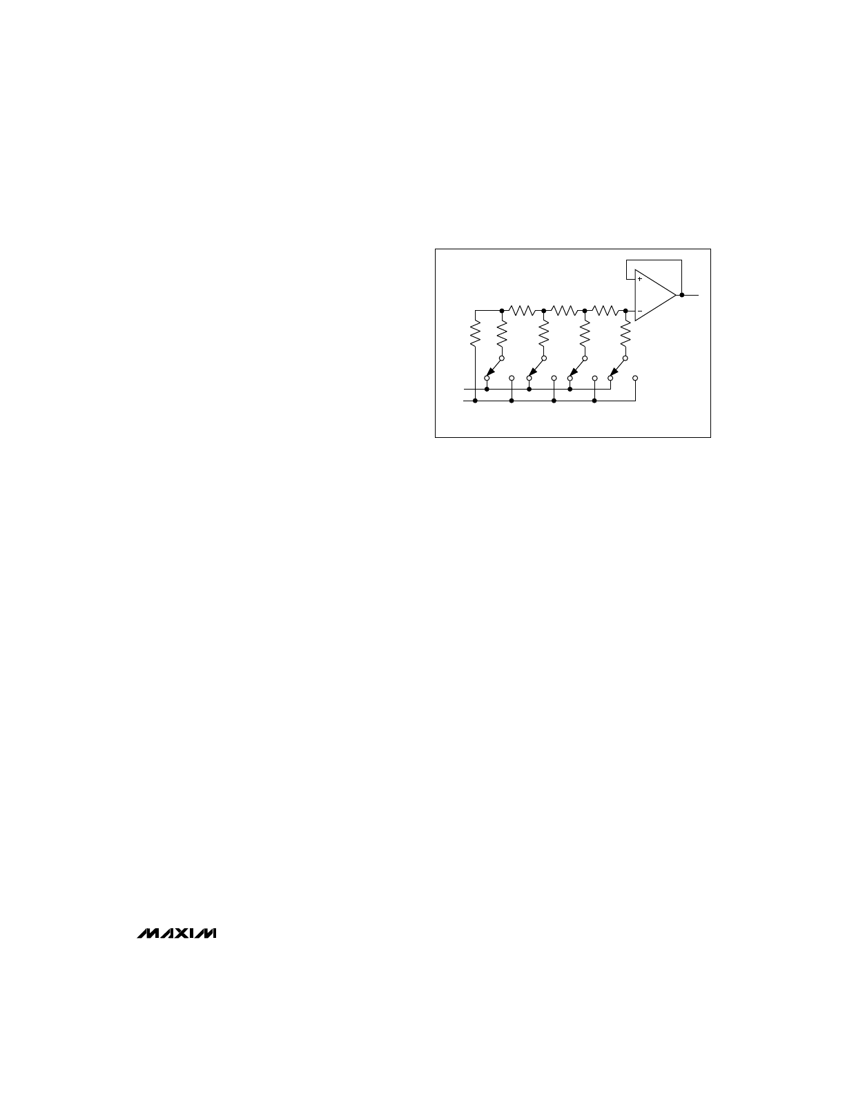
Figure 1. DAC Simplified Circuit Diagram
2R
2R
2R
2R
2R
R
R
R
REF
GND
OUT
SHOWN FOR ALL 1s ON DAC; DAC C IS NOT BUFFERED
SDIN
SCLK
CS
Q2
Q1
SC
SB
SA
LC
LB
LA
D7
D6
D5
D4
D3
D2
D1
D0
OPTIONAL
INSTRUCTION
EXECUTED
(CONTROL BYTE)
(DATA BYTE)
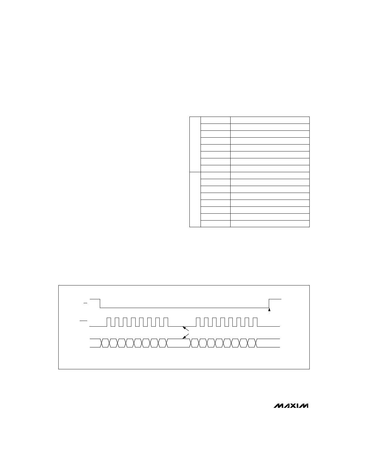
Figure 2. MAX512/MAX513 3-Wire Serial-Interface Timing Diagram
MAX512/MAX513
Low-Cost, Triple, 8-Bit Voltage-Output DACs
with Serial Interface
10
______________________________________________________________________________________
Shutdown Mode
When programmed to shutdown mode, the outputs of
DAC A and B go into a high-impedance state. Virtually
no current flows into or out of the buffer amplifiers in
that state. The output of DAC C goes to 0V when shut
down. In shutdown mode, the REF_ inputs are high
impedance (2M
Ω
typ) to conserve current drain from
the system reference; therefore, the system reference
does not have to be powered down. The logic output
LOUT remains active in shutdown.
Coming out of shutdown, the DAC outputs return to the
values kept in the registers. The recovery time is equiv-
alent to the DAC settling time.
Reset
The
–
R
—
E
—
S
—
E
—
T
–
input is active low. When asserted (
–
R
—
E
—
S
—
E
—
T
–
= 0), DACs A and B are set to full scale (FFhex) and
active, while DAC C is set to zero code (00hex) and
active. The 16-bit serial register is cleared to 0000hex.
LOUT is reset to zero.
Serial Interface
An active-low chip select (
–
C
—
S
–
) enables the shift register
to receive data from the serial data input. Data is
clocked into the shift register on every rising edge of
the serial clock signal (SCLK). The clock frequency can
be as high as 5MHz.
Data is sent MSB first and can be transmitted in one
16-bit word. The write cycle can be interrupted at any
time when
–
C
—
S
–
is kept active (low) to allow, for example,
two 8-bit-wide transfers. After clocking all 16 bits into
the input shift register, the rising edge of
–
C
—
S
–
updates
the DAC outputs, the shutdown status, and the status of
the logic output. Because of their single buffered struc-
ture, DACs cannot be simultaneously updated to differ-
ent digital values.
Table 1. Input Shift Register
*
*
Clocked in last.
**Clocked in first.
Uncommitted Bit
Q2**
Logic Output
Q1
Shut Down DAC C, Active High
SC
Shut Down DAC B, Active High
SB
Shut Down DAC A, Active High
SA
Load Reg DAC C, Active High
LC
Load Reg DAC B, Active High
LB
Load Reg DAC A, Active High
LA
DAC Data Bit 7 (MSB)
B7
DAC Data Bit 6
B6
DAC Data Bit 5
B5
DAC Data Bit 4
B4
DAC Data Bit 3
B3
DAC Data Bit 2
B2
DAC Data Bit 1
B1
DAC Data Bit 0 (LSB)
B0*
DATA BITS
CONTROL BITS
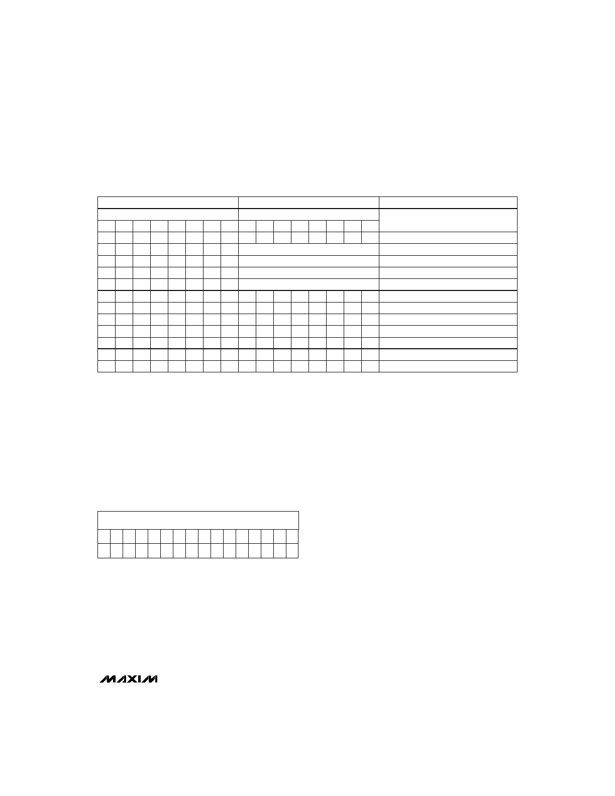
MAX512/MAX513
Low-Cost, Triple, 8-Bit Voltage-Output DACs
with Serial Interface
______________________________________________________________________________________
11
Serial-Input Data Format and Control Codes
Table 2 lists the serial-input data format. The 16-bit
input word consists of an 8-bit control byte and an 8-bit
data byte. The 8-bit control byte is not decoded inter-
nally. Every control bit performs one function. Data is
clocked in starting with Q2 (uncommitted bit), followed
by the remaining control bits and the data byte. The
LSB of the data byte (B0) is the last bit clocked into the
shift register (Figure 2).
Example of a 16-bit input word:
The example above performs the following functions:
• 80hex (128 decimal) loaded into DAC registers
A and B.
• Content of the DAC C register remains unchanged.
• DAC A and DAC B are active.
• DAC C is shut down.
• LOUT is reset to 0.
Digital Inputs
The digital inputs are compatible with CMOS logic.
Supply current increases slightly when toggling the
logic inputs through the transition zone between
(0.3)(V
DD
) and (0.7)(V
DD
).
Digital Output
The latched digital output (LOUT) has a 1.6mA source
capability while maintaining a (V
DD
- 0.4V) output level.
With a 1.6mA sink current, the output voltage is guaran-
teed to be no more than 0.4V. The output can be used
for digital auxiliary control. Please note that the digital
output remains fully active during shutdown mode.
Microprocessor Interfacing
The MAX512/MAX513 serial interface is compatible with
Microwire, SPI, and QSPI. For SPI and QSPI, clear the
CPOL and CPHA bits (CPOL = 0 and CPHA = 0).
CPOL = 0 sets the inactive state of clock to zero and
CPHA = 0 changes data at the falling edge of SCLK.
This setting allows both SPI and QSPI to run at full clock
speeds (0.5MHz and 4MHz, respectively). If a serial port
is not available on your µP, three bits of a parallel port
can be used to emulate a serial port by bit manipulation.
Minimize digital feedthrough at the voltage outputs by
operating the serial clock only when necessary.
CONTROL
DATA
Q2
Q1
SC
SB
SA
LC
LB
LA
B7
B4
B3
B2
B1
B0
FUNCTION
*
*
*
*
*
0
0
0
X
X
X
X
X
X
X
X
No Operation to DAC Registers
*
8-Bit DAC Data
Load Register to DAC C
*
8-Bit DAC Data
Load Register to DAC B
*
8-Bit DAC Data
Load Register to DAC A
*
8-Bit DAC Data
Load All DAC Registers
*
*
0
0
0
*
*
*
X
X
X
X
X
X
X
X
All DACs Active
*
*
1
0
0
*
*
*
X
X
X
X
X
X
X
X
Shut Down DAC C
*
*
0
1
0
*
*
*
X
X
X
X
X
X
X
X
Shut Down DAC B
*
*
0
0
1
*
*
*
X
X
X
X
X
X
X
X
Shut Down DAC A
*
*
1
1
1
*
*
*
X
X
X
X
X
X
X
X
Shut Down All DACs
X
0
*
*
*
*
*
*
X
X
X
X
X
X
X
X
Reset LOUT
X
1
*
*
*
*
*
*
X
X
X
X
X
X
X
X
Set LOUT
B5
B6
Table 2. Serial-Interface Programming Commands
X
Don’t care.
*
Not shown for clarity. The functions of loading and shutting down the DACs and programming the logic can be combined in a single command.
MSB
LSB
1
0
0
1
0
1
1
0
*
0
*
*
*
*
*
*
*
*
0
*
1
*
*
1
*
*
*
*
X
0
1
0
0
0
1
1
1
0
0
0
0
0
0
0
Q2 Q1 SC SB SA LC LB LA B7 B6 B5 B4 B3 B2 B1 B0
Loaded
Loaded
in First
in Last
MAX512/MAX513
Low-Cost, Triple, 8-Bit Voltage-Output DACs
with Serial Interface
12
______________________________________________________________________________________
_____________
Applications Information
Power-Supply and Reference
Operating Ranges
The MAX512 is fully specified to operate with
V
DD
= 5V ±10% and V
SS
= GND = 0V. The MAX513 is
specified for single-supply operation with V
DD
ranging from
2.7V to 3.6V, covering all commonly used supply voltages
in 3V systems. The MAX512/MAX513 can also be used
with a negative supply ranging from -1.5V to -5.5V. Using a
negative supply typically improves zero-code error and
settling time (as shown in the
Typical Operating
Characteristics graphs).
The two separate reference inputs for the DAC pair A/B
and the unbuffered output C allow different full-scale out-
put voltages and, if a negative supply is used, also allow
different polarity. In dual-supply mode, REFAB can vary
from V
SS
to (V
DD
- 1.5V). In single-supply mode, the
specified range for REFAB is 0V to V
DD
. REFC can range
from GND to V
DD
. Do not force REFC below ground.
Power-supply sequencing is not critical. If a negative sup-
ply is used, make sure V
SS
is never more than 0.3V above
ground. Do not apply signals to the digital inputs until the
device is powered-up. If this is not possible, add current-
limiting resistors to the digital inputs.
Power-Supply Bypassing and
Ground Management
In single-supply operation (V
SS
= GND), GND and V
SS
should be connected to the highest quality ground
available. Bypass V
DD
with a 0.1µF to 0.22µF capacitor
to GND. For dual-supply operation, bypass V
SS
with a
0.1µF to 0.22µF capacitor to GND. Reference inputs
can be used without bypassing. For optimum line/load-
transient response and noise performance, bypass the
reference inputs with 0.1µF to 4.7µF to GND. Careful
PC board layout minimizes crosstalk among DAC out-
puts, reference inputs, and digital inputs. Separate ana-
log lines with ground traces between them. Make sure
that high-frequency digital lines are not routed in paral-
lel to analog lines.
Unipolar Output
With unipolar output, the output voltage and the refer-
ence voltage are the same polarity. The MAX512/
MAX513 can be used with a single supply if the refer-
ence voltages are positive. With a negative supply,
t h e
REFAB voltage can vary from V
SS
to
approximately (V
DD
- 1.5V), allowing two-quadrant mul-
tiplication.
CS
SCLK
DIN
LOUT
t
DS
t
OD
t
DH
t
CL
t
CH
t
CSS
t
CSPWH
t
CSH
Figure 3. MAX512/MAX513 Detailed Serial-Interface Timing Diagram
Bipolar Output
Using Figure 4’s circuit, the MAX512/MAX13 can be con-
figured for bipolar outputs. Table 4 lists the bipolar codes
and corresponding output voltages. There are two ways to
achieve rail-to-rail outputs: 1) Operate the
MAX512/MAX513 with a single supply and positive refer-
ence voltages or 2) Use dual supplies with a positive or
negative voltage at REFAB and a positive voltage at REFC.
In either case, the op amps need dual supplies. When
using the dual-supply mode, possible errors associated
with the divide-by-two attenuator and gain-of-two buffer are
eliminated (see the
Output Buffer Amplifier section). For
maximum output swing of all outputs in dual-supply mode,
connect REFAB to V
SS
and REFC to V
DD
. In single-supply
mode, connect REFAB, REFC, and V
DD
together.
With dual supplies, DACs A and B can perform four-
quadrant multiplication. Please note that in dual-supply
mode, the REFAB input ranges from V
SS
to (V
DD
-
1.5V). Because REFC accepts only positive inputs,
DAC C performs two-quadrant multiplication.
Figure 4 shows Maxim’s ICL7612A with rail-to-rail input
common-mode range and rail-to-rail output voltage
swing—ideal for a high output voltage swing from low
supply voltages.
RF Applications
Both the MAX512 and MAX513 can bias GaAs FETs,
where the gate of the FETs must be negatively biased
to ensure that there is no drain current. In a typical
application, power to the RF amplifiers should not be
turned on until the bias voltages provided by DAC A
and DAC B are fully established; likewise, the supply
should be turned off before the bias voltage is switched
off. Figure 5 shows how DAC B supplies the negative
bias V
GG1
for the driver stage and DAC A provides the
negative bias V
GG2
for the output stage [1].
The DAC A and DAC B outputs are also ideal for con-
trolling VCOs in mobile radios or cellular phones. Other
applications include varactor and PIN diode circuits.
The unbuffered DAC C provides a span within GND
and V
DD
and is individually set at REF C. DAC C typi-
cally adjusts offset and gain in the system.
1 [John Wachsmann. “A High-Efficiency GaAs MMIC Power Amplifier for
1.9GHz PCS Applications,” Proceedings of the First Annual Wireless
Symposium, pp. 375, Penton Publishing, Jan. 1993.]
MAX512/MAX513
Low-Cost, Triple, 8-Bit Voltage-Output DACs
with Serial Interface
______________________________________________________________________________________
13
DAC CONTENTS
B7 B6 B5 B4 B3 B2 B1 B0
ANALOG
OUTPUT
1
1
1
1
1
1
1
1
+
×
REF_
255
256
1
0
0
0
0
0
0
1
+
×
REF_
129
256
1
0
0
0
0
0
0
0
+
×
= +
REF_
128
256
REF_
2
0
1
1
1
1
1
1
1
+
×
REF_
127
256
0
0
0
0
0
0
0
1
+
×
REF_
1
256
0
0
0
0
0
0
0
0
0V
Note :
1LSB
REF_
2
REF_
1
256
ANALOG OUTPUT
REF_
D
256
8
=
×
=
×
=
×
−
Table 3. Unipolar Code Table
DAC CONTENTS
B7 B6 B5 B4 B3 B2 B1 B0
ANALOG
OUTPUT
1
1
1
1
1
1
1
1
+
×
REF_
127
128
1
0
0
0
0
0
0
1
+
×
REF_
1
128
0
1
1
1
1
1
1
1
−
×
REF_
1
128
0
0
0
0
0
0
0
1
−
×
REF_
127
128
0
0
0
0
0
0
0
0
−
×
−
REF_
128
128
= REF_
1
0
0
0
0
0
0
0
0V
Note :
1LSB
REF_
2
REF_
1
128
ANALOG OUTPUT
REF_
D
128
1
8 - 1)
=
×
=
×
=
×
−
−
(
Table 4. Bipolar Code Table
MAX512/MAX513
Low-Cost, Triple, 8-Bit Voltage-Output DACs
with Serial Interface
14
______________________________________________________________________________________
DAC B
DAC A
OUTA
OUTB
MAX512
MAX513
0.05
µ
F
0.01
µ
F
V
GG1
V
DD1
V
DD2
V
GG2
RF
OUT
RF
IN
REFAB = -4.2V
Figure 5. RF Bias Circuit
DAC
LATCH
A
DAC A
DAC
LATCH
B
DAC B
DAC
LATCH
C
LATCH
DAC C
SCLK
OUTA
OUTB
OUTC
LOUT
DIN
CS
REFAB
REFC
RESET
V
DD
V
DD
V
DD
V
OUT
V
OUT
V
SS
V
DD
V
SS
V
SS
V
SS
GND
16-BIT SHIFT REGISTER
CONTROL (8)
DATA (8)
MAX512
MAX513
1
2
4
5
6
7
8
9
10
11
12
3
14
0.22
µ
F
0.22
µ
F
0.1
µ
F
0.1
µ
F
0.1
µ
F
0.1
µ
F
0.05
µ
F
0.1
µ
F
R*
R*
** CONNECT PIN 8 TO GND
ICL7612A**
ICL7612A**
* R IN 10k
Ω
RANGE
R*
R*
Figure 4. Bipolar Output Circuit
MAX512/MAX513
Low-Cost, Triple, 8-Bit Voltage-Output DACs
with Serial Interface
______________________________________________________________________________________
15
_Ordering Information (continued)
___________________Chip Topography
SCLK
RESET
REFC
REFAB
OUTC
OUTA
GND
OUTB
V
SS
CS
LOUT
DIN
0.122"
(3.099mm)
0.081"
(2.057mm)
V
DD
TRANSISTOR COUNT: 1910
SUBSTRATE CONNECTED TO V
DD
* Contact factory for dice specifications.
Dice*
0°C to +70°C
MAX513C/D
14 SO
0°C to +70°C
MAX513CSD
14 Plastic DIP
0°C to +70°C
MAX513
CPD
14 CERDIP
-55°C to +125°C
MAX513MJD
14 SO
-40°C to +85°C
MAX513ESD
14 Plastic DIP
-40°C to +85°C
MAX513EPD
14 CERDIP
-55°C to +125°C
MAX512MJD
14 SO
-40°C to +85°C
MAX512ESD
14 Plastic DIP
-40°C to +85°C
MAX512EPD
PIN-PACKAGE
TEMP. RANGE
PART
Maxim cannot assume responsibility for use of any circuitry other than circuitry entirely embodied in a Maxim product. No circuit patent licenses are
implied. Maxim reserves the right to change the circuitry and specifications without notice at any time.
16
__________________Maxim Integrated Products, 120 San Gabriel Drive, Sunnyvale, CA 94086 (408) 737-7600
© 1996 Maxim Integrated Products
Printed USA
is a registered trademark of Maxim Integrated Products.
MAX512/MAX513
Low-Cost, Triple, 8-Bit Voltage-Output DACs
with Serial Interface
________________________________________________________Package Information
C
A
A2
E1
D
E
e
A
e
B
A3
B1
B
DIM
A
A1
A2
A3
B
B1
C
D
D1
E
E1
e
e
A
e
B
L
α
MIN
–
0.015
0.125
0.055
0.016
0.050
0.008
0.735
0.050
0.300
0.240
–
0.115
0˚
MAX
0.200
–
0.150
0.080
0.022
0.065
0.012
0.765
0.080
0.325
0.280
0.400
0.150
15˚
MIN
–
0.38
3.18
1.40
0.41
1.27
0.20
18.67
1.27
7.62
6.10
–
2.92
0˚
MAX
5.08
–
3.81
2.03
0.56
1.65
0.30
19.43
2.03
8.26
7.11
10.16
3.81
15˚
INCHES
MILLIMETERS
2.54 BSC
7.62 BSC
0.100 BSC
0.300 BSC
A1
L
D1
e
21-330A
α
14-PIN PLASTIC
DUAL-IN-LINE
PACKAGE
L
DIM
A
A1
B
C
D
E
e
H
h
L
α
MIN
0.053
0.004
0.014
0.007
0.337
0.150
0.228
0.010
0.016
0˚
MAX
0.069
0.010
0.019
0.010
0.344
0.157
0.244
0.020
0.050
8˚
MIN
1.35
0.10
0.35
0.19
8.55
3.80
5.80
0.25
0.40
0˚
MAX
1.75
0.25
0.49
0.25
8.75
4.00
6.20
0.50
1.27
8˚
INCHES
MILLIMETERS
α
14-PIN PLASTIC
SMALL-OUTLINE
PACKAGE
H
E
D
e
A
A1
C
h x 45˚
0.127mm
0.004in.
B
1.27 BSC
0.050 BSC
21-331A