
_______________General Description
The MAX509/MAX510 are quad, serial-input, 8-bit volt-
age-output digital-to-analog converters (DACs). They
operate with a single +5V supply or dual ±5V supplies.
Internal, precision buffers swing rail-to-rail. The refer-
ence input range includes both supply rails.
The MAX509 has four separate reference inputs, allow-
ing each DAC's full-scale range to be set independently.
20-pin DIP, SSOP, and SO packages are available. The
MAX510 is identical to the MAX509 except it has two ref-
erence inputs, each shared by two DACs. The MAX510
is housed in space-saving 16-pin DIP and SO packages.
The serial interface is double-buffered: A 12-bit input
shift register is followed by four 8-bit buffer registers and
four 8-bit DAC registers. A 12-bit serial word is used to
load data into each register. Both input and DAC regis-
ters can be updated independently or simultaneously
with single software commands. Two additional asyn-
chronous control pins provide simultaneous updating
(
LDAC) or clearing (CLR) of input and DAC registers.
The interface is compatible with Microwire
TM
and SPI/
QSPI
TM
. All digital inputs and outputs are TTL/CMOS
compatible. A buffered data output provides for read-
back or daisy-chaining of serial devices.
____________________________Features
♦
Single +5V or Dual ±5V Supply Operation
♦
Output Buffer Amplifiers Swing Rail-to-Rail
♦
Reference Input Range Includes Both Supply Rails
♦
Calibrated Offset, Gain, and Linearity (1LSB TUE)
♦
10MHz Serial Interface, Compatible with SPI, QSPI
(CPOL = CPHA = 0) and Microwire
♦
Double-Buffered Registers for Synchronous
Updating
♦
Serial Data Output for Daisy-Chaining
♦
Power-On Reset Clears Serial Interface and Sets
All Registers to Zero
______________Ordering Information
Ordering Information continued on last page.
* Dice are specified at +25°C, DC parameters only.
**Contact factory for availability and processing to MIL-STD-883.
MAX509/MAX510
Quad, Serial 8-Bit DACs
with Rail-to-Rail Outputs
________________________________________________________________
Maxim Integrated Products
1
20
19
18
17
16
15
14
13
12
11
1
2
3
4
5
6
7
8
9
10
OUTC
OUTD
V
DD
REFC
REFB
V
SS
OUTA
OUTB
TOP VIEW
MAX509
REFD
CS
N.C.
SCLK
DGND
N.C.
AGND
REFA
DIN
CLR
DOUT
LDAC
DIP/SO/SSOP
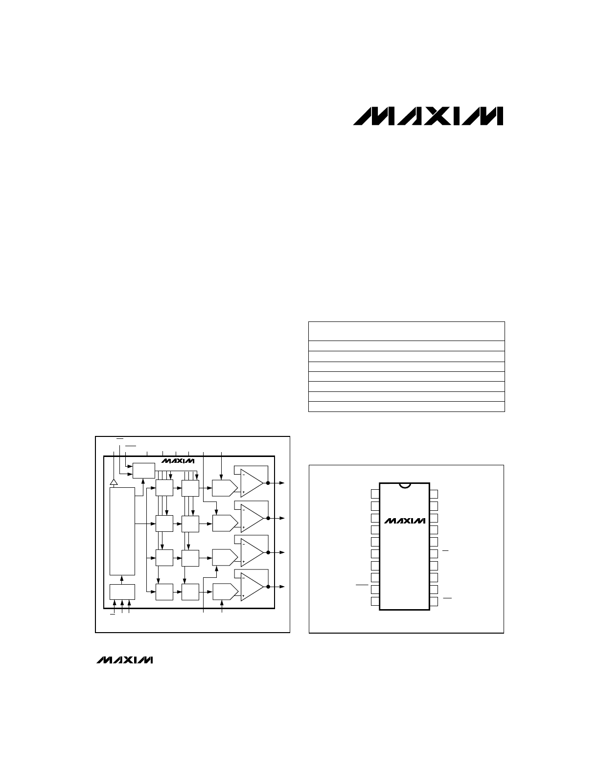
_________________Pin Configurations
MAX509
OUTA
DAC A
DAC B
DAC C
DAC D
REFA
REFB
DAC
REG A
DECODE
CONTROL
INPUT
REG A
DAC
REG B
INPUT
REG B
DAC
REG C
INPUT
REG C
DAC
REG D
INPUT
REG D
12-BIT
SHIFT
REGISTER
SR
CONTROL
CS DIN SCLK
REFC
REFD
OUTB
OUTC
OUTD
DOUT
LDAC
CLR
V
DD
DGND V
SS
AGND
_______________Functional Diagrams
19-0155; Rev 2; 1/96
PART
TEMP. RANGE
PIN-PACKAGE
MAX509
ACPP
0°C to +70°C
20 Plastic DIP
MAX509BCPP
0°C to +70°C
20 Plastic DIP
MAX509ACWP
0°C to +70°C
20 Wide SO
±1
±1 1/2
±1
MAX509BCWP
20 Wide SO
±1 1/2
MAX509ACAP
0°C to +70°C
20 SSOP
±1
0°C to +70°C
MAX509BCAP
0°C to +70°C
20 SSOP
±1 1/2
MAX509BC/D
0°C to +70°C
Dice*
±1 1/2
Pin Configurations continued at end of data sheet.
Functional Diagrams continued at end of data sheet.
TUE
(LSB)
Microwire is a trademark of National Semiconductor. SPI and QSPI are trademarks of Motorola.
For free samples & the latest literature: http://www.maxim-ic.com, or phone 1-800-998-8800
MAX509/MAX510
Quad, Serial 8-Bit DACs
with Rail-to-Rail Outputs
2
_______________________________________________________________________________________
V
DD
to DGND ..............................................................-0.3V, +6V
V
DD
to AGND...............................................................-0.3V, +6V
V
SS
to DGND ...............................................................-6V, +0.3V
V
SS
to AGND ...............................................................-6V, +0.3V
V
DD
to V
SS
.................................................................-0.3V, +12V
Digital Input Voltage to DGND ......................-0.3V, (V
DD
+ 0.3V)
REF_....................................................(V
SS
- 0.3V), (V
DD
+ 0.3V)
OUT_..............................................................................V
DD
, V
SS
Maximum Current into Any Pin............................................50mA
Continuous Power Dissipation (T
A
= +70°C)
16-Pin Plastic DIP (derate 10.53mW/°C above +70°C) ....842mW
16-Pin Wide SO (derate 9.52mW/°C above +70°C) .........762mW
16-Pin CERDIP (derate 10.00mW/°C above +70°C) ........800mW
20-Pin Plastic DIP (derate 11.11mW/°C above +70°C)....889mW
20-Pin Wide SO (derate 10.00mW/°C above +70°C) .......800mW
20-Pin SSOP (derate 10.00mW/°C above +70°C) ............800mW
20-Pin CERDIP (derate 11.11mW/°C above +70°C) ........889mW
Operating Temperature Ranges:
MAX5_ _ _C_ _ .....................................................0°C to +70°C
MAX5_ _ _E_ _ ..................................................-40°C to +85°C
MAX5_ _ _MJ_ ................................................-55°C to +125°C
Storage Temperature Range .............................-65°C to +150°C
Lead Temperature (soldering, 10sec) .............................+300°C
ELECTRICAL CHARACTERISTICS
(VDD = +5V ±10%, VSS = 0V to -5.5V, VREF = 4V, AGND = DGND = 0V, RL = 10k
Ω
, CL = 100pF, TA = TMIN to TMAX,
unless otherwise noted.)
Stresses beyond those listed under “Absolute Maximum Ratings” may cause permanent damage to the device. These are stress ratings only, and functional
operation of the device at these or any other conditions beyond those indicated in the operational sections of the specifications is not implied. Exposure to
absolute maximum rating conditions for extended periods may affect device reliability.
PARAMETER
CONDITIONS
MIN
TYP
MAX
UNITS
Note:
The outputs may be shorted to VDD, VSS, or AGND if the package power dissipation is not exceeded. Typical short-circuitcurrent
to AGND is 50mA. Do not bias AGND more than +1V above DGND, or more than 2.5V below DGND.
ABSOLUTE MAXIMUM RATINGS
Resolution
8
Bits
±1
MAX5_ _A
VREF = +4V,
VSS = 0V or -5V ±10%
MAX5_ _B
±1
MAX5_ _A
Total Unadjusted Error
VREF = -4V,
VSS = -5V ±10%
±1.5
LSB
Differential Nonlinearity
±1
LSB
Guaranteed monotonic
14
MAX5_ _C
16
MAX5_ _E
MAX5_ _B
±10
µV/°C
Code = FF hex
1
4
MAX5_ _C
Full-Scale Error
±14
mV
Code = FF hex
±10
µV/°C
Code = 00 hex
Zero-Code-Error Supply Rejection
1
2
mV
Code = 00 hex,
VSS = 0V
20
MAX5_ _M
SYMBOL
TUE
DNL
±14
MAX5_ _C
±16
MAX5_ _E
Zero-Code Error
Code = 00 hex,
VSS = -5V ±10%
±20
mV
MAX5_ _M
ZCE
±1.5
Code = 00 hex, V
DD
= 5V ±10%,
V
SS
= 0V or -5V ±10%
Zero-Code
Temperature Coefficient
1
8
MAX5_ _E
Full-Scale-Error Supply Rejection
Code = FF hex,
V
DD
= +5V ±10%,
V
SS
= 0V or -5V ±10%
1
12
mV
MAX5_ _M
Full-Scale-Error
Temperature Coefficient
STATIC ACCURACY
MAX509/MAX510
Quad, Serial 8-Bit DACs
with Rail-to-Rail Outputs
_______________________________________________________________________________________
3
ELECTRICAL CHARACTERISTICS (continued)
(VDD = +5V ±10%, VSS = 0V to -5.5V, VREF = 4V, AGND = DGND = 0V, RL = 10k
Ω
, CL = 100pF, TA = TMIN to TMAX,
unless otherwise noted.)
PARAMETER
CONDITIONS
MIN
TYP
MAX
UNITS
Input Voltage Range
SYMBOL
V
SS
V
DD
V
MAX509
16
24
MAX510
Input Resistance (Note 1)
8
12
k
Ω
Code = 55 hex
MAX509
15
(Note 4)
AC Feedthrough
-70
dB
(Note 3)
Channel-to-Channel Isolation
-60
dB
MAX510
Input Capacitance (Note 2)
30
pF
Code = 00 hex
10
2
VREF = 4V, load regulation
≤
1/4LSB
2
Full-Scale Output Voltage
V
SS
V
DD
V
Resistive Load
10
k
Ω
Input High Voltage
2.4
V
V
IH
VREF = -4V, V
SS
= -5V ±10%,
load regulation
≤
1/4LSB
VREF = V
DD
MAX5_ _C/E,
load regulation
≤
1LSB
VREF = V
DD
MAX5_ _M,
load regulation
≤
2LSB
Input Low Voltage
0.8
V
V
IL
V
IN
= 0V or V
DD
Input Current
1.0
µA
I
IN
(Note 5)
Input Capacitance
10
pF
C
IN
I
SOURCE
= 0.2mA
Output High Voltage
V
DD
- 0.5
V
V
OH
I
SINK
= 1.6mA
Output Low Voltage
0.4
V
V
OL
MAX5_ _E
0.7
MAX5_ _C
1.0
MAX5_ _M
Voltage-Output Slew Rate
0.5
V/µs
Positive and negative
To 1/2LSB, 10k
Ω
II 100pF load
Output Settling Time (Note 6)
6
µs
Digital Feedthrough
5
nV-s
Wideband Amplifier Noise
60
MHz
VREF = 0.5V
p-p
, 3dB bandwidth
Multiplying Bandwidth
1
VREF = 4V
p-p
at 1kHz, V
DD
= 5V,
code = FF hex
Digital-to-Analog Glitch Impulse
87
Code 128➝127
12
nV-s
Code = 00 hex, all digital inputs
from 0V to V
DD
Signal-to-Noise + Distortion Ratio
VREF = 4V
p-p
at 20kHz, V
SS
= -5V ±10%
74
dB
SINAD
µV
RMS
REFERENCE INPUTS
DAC OUTPUTS
DIGITAL INPUTS
DIGITAL OUTPUTS
DYNAMIC PERFORMANCE
MAX509/MAX510
Quad, Serial 8-Bit DACs
with Rail-to-Rail Outputs
4
_______________________________________________________________________________________
ELECTRICAL CHARACTERISTICS (continued)
(VDD = +5V ±10%, VSS = 0V to -5.5V, VREF = 4V, AGND = DGND = 0V, RL = 10k
Ω
, CL = 100pF, TA = TMIN to TMAX,
unless otherwise noted.)
PARAMETER
CONDITIONS
MIN
TYP
MAX
UNITS
Positive Supply Voltage
SYMBOL
4.5
5.5
V
For specified performance
V
DD
Negative Supply Voltage
-5.5
0
V
For specified performance
V
SS
5
10
Positive Supply Current
5
12
mA
I
DD
Negative Supply Current
mA
I
SS
5
10
MAX5_ _C/E
MAX5_ _M
MAX5_ _C/E
5
12
MAX5_ _M
V
SS
= -5V ±10%, outputs
unloaded, all digital
inputs = 0V or V
DD
Note 1:
Input resistance is code dependent. The lowest input resistance occurs at code = 55 hex.
Note 2:
Input capacitance is code dependent. The highest input capacitance occurs at code = 00 hex.
Note 3:
VREF = 4V
p-p
, 10kHz. Channel-to-channel isolation is measured by setting the code of one DAC to FF hex and setting the
code of all other DACs to 00 hex.
Note 4:
VREF = 4V
p-p
, 10kHz. DAC code = 00 hex.
Note 5:
Guaranteed by design.
Note 6:
Output settling time is measured by taking the code from 00 hex to FF hex, and from FF hex to 00 hex.
TIMING CHARACTERISTICS
(VDD = +5V ±10%, VSS = 0V to -5V, VREF = 4V, AGND = DGND = 0V, CL = 50pF, TA = TMIN to TMAX, unless otherwise noted.)
PARAMETER
CONDITIONS
MIN
TYP
MAX
UNITS
CLR Pulse Width Low
SYMBOL
50
25
ns
MAX5_ _M
MAX5_ _C/E
40
20
t
CLW
MAX5_ _M
50
25
ns
MAX5_ _C/E
40
20
SCLK Fall to
CS Rise Hold Time
0
ns
t
CSH2
SCLK Fall to
CS Fall Hold Time
0
ns
(Note 7)
t
CSH0
40
MAX5_ _C/E
10
100
MAX5_ _C/E
MAX5_ _C/E
40
40
MAX5_ _C/E
20
12.5
MAX5_ _C/E
DIN to SCLK Rise Hold Time
0
ns
t
DH
SCLK Rise to
CS Rise Hold Time
(Note 9)
40
ns
t
CSH1
LDAC Pulse Width Low
(Notes 7, 8)
0
ns
t
LDW
t
CLL
CS Rise to LDAC Fall Setup Time
40
MAX5_ _C/E
CS Fall to SCLK Setup Time
50
ns
MAX5_ _M
t
CSS
DIN to SCLK Rise Setup Time
50
ns
MAX5_ _M
t
DS
SCLK Clock Frequency
20
10
MHz
MAX5_ _M
f
CLK
SCLK Pulse Width High
50
ns
MAX5_ _M
t
CH
SCLK Pulse Width Low
MAX5_ _M
50
ns
t
CL
SCLK to DOUT Valid
10
100
ns
MAX5_ _M
t
DO
Note 7:
Guaranteed by design.
Note 8:
If
LDAC is activated prior to CS's rising edge, it must stay low for t
LDW
or longer after
CS goes high.
Note 9:
Minimum delay from 12th clock cycle to
CS rise.
Outputs unloaded, all
digital inputs = 0V or V
DD
POWER SUPPLIES
SERIAL INTERFACE TIMING
MAX509/MAX510
Quad, Serial 8-Bit DACs
with Rail-to-Rail Outputs
_______________________________________________________________________________________
5
12
0
0
1.2
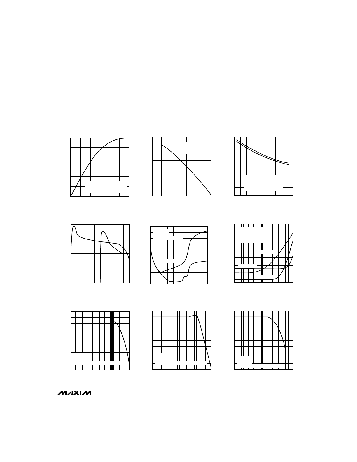
OUTPUT SINK CURRENT
vs. (V
OUT
- V
SS
)
2
10
MAX509-FG01
V
OUT
- V
SS
(V)
I
OUT
(mA)
0.8
6
4
0.2
0.6
1.0
8
0.4
V
DD
= VREF = +5V
V
SS
= GND = 0V
ALL DIGITAL INPUTS = 00 HEX
-25
0
3.6
4.6
-20
MAX509-FG10
V
OUT
(V)
I
OUT
(mA)
4.4
-10
-5
3.8
4.0
-15
OUTPUT SOURCE CURRENT
vs. OUTPUT VOLTAGE
4.8
5.0
4.2
V
DD
= VREF = +5V
V
SS
= GND
DIGITAL INPUT = FF HEX
7
0
-60
-20
40
100
SUPPLY CURRENT
vs. TEMPERATURE
2
6
MAX509-FG02
TEMPERATURE (
°
C)
SUPPLY CURRENT (mA)
20
80
4
5
3
1
-40
0
60
120 140
I
DD
I
SS
V
DD
= +5.5V
V
SS
= -5.5V
VREF = -4.75
ALL DIGITAL INPUTS = +5V
6
0
-5
5
SUPPLY CURRENT
vs. REFERENCE VOLTAGE
1
5
MAX509-FG03
VREF VOLTAGE (V)
I
DD
(mA)
0
3
2
-4
-2
2
4
4
3
1
-1
-3
V
DD
= +5V
ALL LOGIC
INPUTS = +5V
V
SS
= -5V
V
SS
= 0V
0
1k
10k
100k
REFERENCE VOLTAGE INPUT
FREQUENCY RESPONSE
-40
MAX509-FG06
FREQUENCY (Hz)
RELATIVE OUTPUT (dB)
-30
-20
-10
1M
10M
V
DD
= +5V
V
SS
= AGND
VREF = 2.5VDC + 0.5Vp-p SINE WAVE
-40
-90
0
2
6
10
THD + NOISE AT DAC OUTPUT
vs. REFERENCE AMPLITUDE
-80
-50
MAX509-FG04
REFERENCE AMPLITUDE (Vp-p)
THD + NOISE (dB)
4
8
-60
-70
-85
-75
-65
-55
-45
1%
0.01%
0.1%
FREQ = 20kHz
FREQ = 1kHz
V
DD
= +5V
V
SS
= -5V
INPUT CODE = FF HEX
THD + NOISE (%)
-20
-80
10
1k
100k
THD + NOISE AT DAC OUTPUT
vs. REFERENCE FREQUENCY
-70
MAX509-FG05
REFERENCE FREQUENCY (Hz)
THD + NOISE (dB)
-60
-50
-40
-90
-30
100
10k
VREF = 8Vp-p
VREF = 1Vp-p
VREF = 4Vp-p
V
DD
= +5V
V
SS
= -5V
INPUT CODE = FF HEX
FREQ = SWEPT
10%
1%
0.1%
0.01%
THD + NOISE (%)
0
1k
10k
100k
REFERENCE VOLTAGE INPUT
FREQUENCY RESPONSE
-40
MAX509-FG07
FREQUENCY (Hz)
RELATIVE OUTPUT (dB)
-30
-20
-10
1M
10M
V
DD
= +5V
V
SS
= AGND
VREF = 2.5VDC + 0.05Vp-p SINE WAVE
0
1k
10k
100k
REFERENCE VOLTAGE INPUT
FREQUENCY RESPONSE
-40
MAX509-FG08
FREQUENCY (Hz)
RELATIVE OUTPUT (dB)
-30
-20
-10
1M
10M
V
DD
= +5V
V
SS
= -5V
VREF = 2.5VDC + 4Vp-p SINE WAVE
__________________________________________Typical Operating Characteristics
(T
A
= +25°C, unless otherwise noted.)
MAX509/MAX510
Quad, Serial 8-DACs
with Rail-to-Rail Outputs
6
_______________________________________________________________________________________
____________________________Typical Operating Characteristics (continued)
(T
A
= +25°C, unless otherwise noted.)
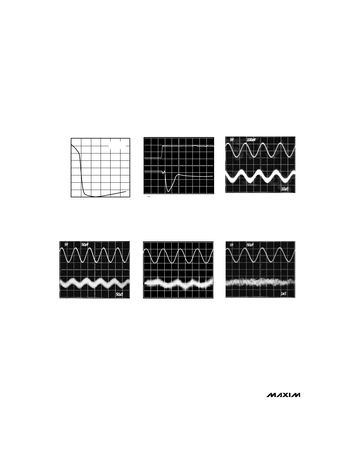
A = REFA, 10V
p-p
B = OUTA, 100
µ
V/div, UNLOADED
TIMEBASE = 10
µ
s/div
V
DD
= +5V, V
SS
= -5V
CODE = ALL 0s
REFERENCE FEEDTHROUGH AT 40kHz
A
B
A = REFA, 10V
p-p
B = OUTA, 50
µ
V/div, UNLOADED
TIMEBASE = 1ms/div
REFERENCE FEEDTHROUGH AT 400Hz
A
B
A = REFA, 10V
p-p
B = OUTA, 50
µ
V/div, UNLOADED
TIMEBASE = 50
µ
s/div
REFERENCE FEEDTHROUGH AT 10kHz
A
B
5V
50µV
100µS
A = REFA, 10V
p-p
B = OUTA, 50
µ
V/div, UNLOADED
TIMEBASE = 100
µ
s/div
REFERENCE FEEDTHROUGH AT 4kHz
A
B
10
5.0
3.6
0
-4
ZERO-CODE ERROR
vs. NEGATIVE SUPPLY VOLTAGE
3.8
4.8
MAX509-FG09
V
SS
(V)
ZERO-CODE ERROR (mV)
-3
4.4
4.0
-1
-2
4.6
3.4
4.2
-5
-6
V
DD
= +5V
VREF = +4V
A = CS, 2V/div
B = OUTA, 20mV ˜
TIMEBASE = 200ns/div
WORST-CASE 1LSB DIGITAL STEP CHANGE
A
B
200nS
2V
20mV
MAX509/MAX510
Quad, Serial 8-Bit DACs
with Rail-to-Rail Outputs
_______________________________________________________________________________________
7
5V
100mV
1µS
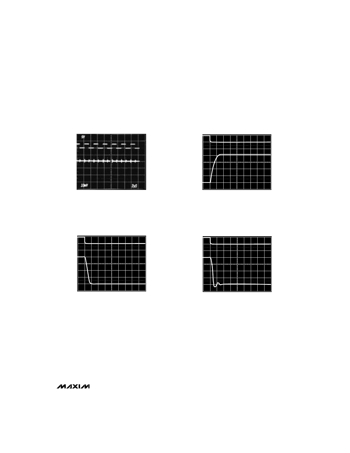
A = DIGITAL INPUT, 5V/div
B = OUT_ , 2V/div
TIMEBASE = 1
µ
s/div
V
DD
= +5V
REF_ = +4V
ALL BITS OFF TO ALL BITS ON
R
L
= 10k
Ω
, C
L
= 100pF
POSITIVE SETTLING TIME
(V
SS
= AGND OR -5V)
A
B
5V
100mV
1µS
A = DIGITAL INPUT, 5V/div
B = OUT_ , 2V/div
TIMEBASE = 1
µ
s/div
V
DD
= +5V
REF_ = +4V
ALL BITS ON TO ALL BITS OFF
R
L
= 10k
Ω
, C
L
= 100pF
NEGATIVE SETTLING TIME
(V
SS
= AGND)
A
B
____________________________Typical Operating Characteristics (continued)
(T
A
= +25°C, unless otherwise noted.)
A = SCLK, 333kHz
B = OUT_, 10mV/div
TIMEBASE = 2
µ
s/div
CLOCK FEEDTHROUGH
A
B
5V
100mV
1µS
A = DIGITAL INPUT, 5V/div
B = OUT_ , 2V/div
TIMEBASE = 1
µ
s/div
V
DD
= +5V
REF_ = +4V
ALL BITS ON TO ALL BITS OFF
R
L
= 10k
Ω
, C
L
= 100pF
NEGATIVE SETTLING TIME
(V
SS
= -5V)
A
B
MAX509/MAX510
Quad, Serial 8-Bit DACs
with Rail-to-Rail Outputs
8
_______________________________________________________________________________________
NAME
FUNCTION
1
OUTB
DAC B Voltage Output
2
OUTA
DAC A Voltage Output
3
V
SS
Negative Power Supply, 0V to -5V ±10%. Connect to AGND for single-supply operation.
PIN
MAX509
MAX510
1
2
4
REFB
Reference Voltage Input for DAC B
–
REFAB
Reference Voltage Input for DACs A and B
5
REFA
Reference Voltage Input for DAC A
6
AGND
Analog Ground
3
–
4
7, 14
N.C.
Not Internally Connected
8
DGND
Digital Ground
–
5
–
6
______________________________________________________________Pin Description
10
DOUT
8
9
LDAC
7
11
CLR
9
12
DIN
10
13
SCLK
11
15
CS
12
16
REFD
Reference Voltage Input for DAC D
–
–
REFCD
Reference Voltage Input for DACs C and D
13
Load DAC Input (active low). Driving this asynchronous input low (level sensitive)
transfers the contents of each input latch to its respective DAC latch.
Serial Data Output. Can sink and source current. Data at DOUT is adjustable to be
clocked out on rising or falling edge of SCLK.
17
REFC
Reference Voltage Input for DAC C
–
18
V
DD
Positive Power Supply, +5V ±10%
14
19
OUTD
DAC D Output Voltage
15
20
OUTC
DAC C Output Voltage
16
Clear DAC input (active low). Driving
CLR low causes an asynchronous clear of input
and DAC registers and sets all DAC outputs to zero.
Serial Data Input. TTL/CMOS-compatible input. Data is clocked into DIN on the
rising edge of SCLK.
CS must be low for data to be clocked in.
Serial Clock Input. Data is clocked in on the rising edge and clocked out on either the
rising (default) or the falling edge.
Chip-Select Input (active low). Data is shifted in and out when
CS is low. Programming
commands are executed when
CS rises.
MAX509/MAX510
Quad, Serial 8-Bit DACs
with Rail-to-Rail Outputs
_______________________________________________________________________________________
9
• • •
• • •
• • •
• • •
A1 A0
C1 C0
D7 D6
D5 D4 D3 D2 D1 D0
MSB
LSB
DACA
DATA FROM PREVIOUS DATA INPUT
DATA FROM PREVIOUS DATA INPUT
A1 A0
C1 C0
D7
D6 D5 D4 D3 D2
D1 D0
MSB
LSB
DACD
A1
A1
A1
A1
A0
C1
C0
D7
D6 D5 D4 D3 D2 D1 D0
A1
A0
C1 C0
D7
A0
C1 C0
D7
D6 D5 D4 D3 D2 D1
D0
A1
A1
A0 C1
C0
D7
D6 D5
D4 D3 D2
D1 D0
A1
D6
D5 D4 D3 D2 D1 D0
A1
A1
DOUT
MODE 0
DOUT
MODE 1
(DEFAULT)
DIN
SCLK
• • •
CS
INSTRUCTION
EXECUTED
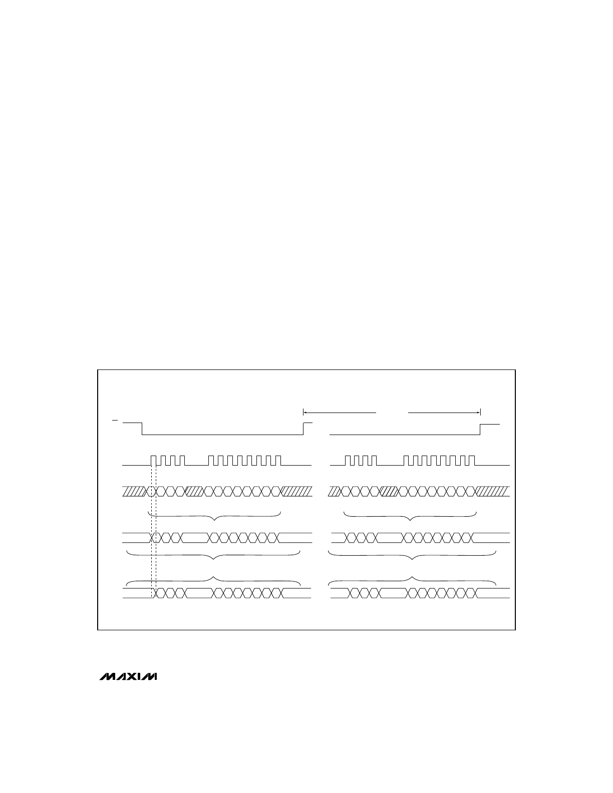
Figure 1. MAX509/MAX510 3-Wire Interface Timing
_______________Detailed Description
Serial Interface
At power-on, the serial interface and all DACs are
cleared and set to code zero. The serial data output
(DOUT) is set to transition on SCLK's rising edge.
The MAX509/MAX510 communicate with microproces-
sors through a synchronous, full-duplex, 3-wire inter-
face (Figure 1). Data is sent MSB first and can be
transmitted in one 4-bit and one 8-bit (byte) packet or
in one 12-bit word. If a 16-bit control word is used, the
first four bits are ignored. A 4-wire interface adds a line
for
LDAC and allows asynchronous updating. The serial
clock (SCLK) synchronizes the data transfer. Data is
transmitted and received simultaneously.
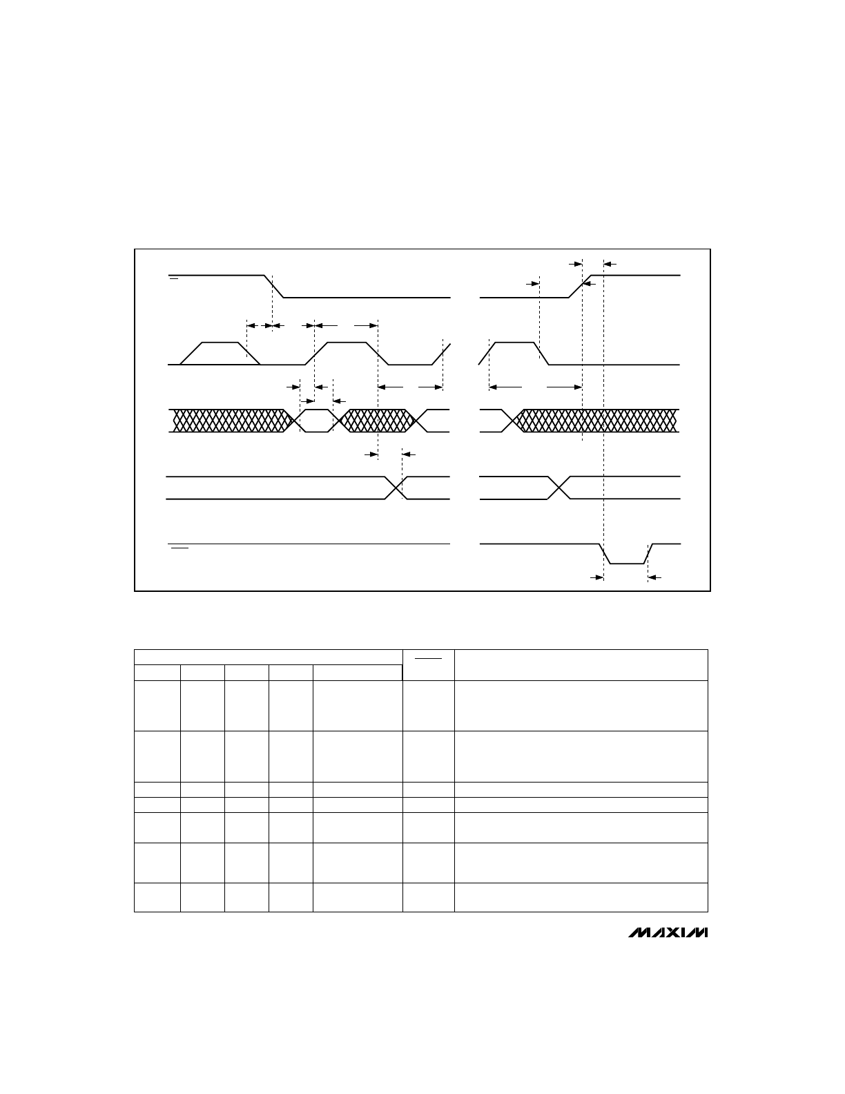
Figure 2 shows a detailed serial interface timing.
Please note that the clock should be low if it is stopped
between updates. DOUT does not go into a high-
impedance state if the clock or
CS is high.
Serial data is clocked into the data registers in MSB-
first format, with the address and configuration infor-
mation preceding the actual DAC data. Data is
clocked in on SCLK's rising edge while
CS is low. Data
at DOUT is clocked out 12 clock cycles later, either at
SCLK's rising edge (default or mode 1) or falling edge
(mode 0).
Chip select (
CS) must be low to enable the DAC. If CS
is high, the interface is disabled and DOUT remains
unchanged.
CS must go low at least 40ns before the
first rising edge of the clock pulse to properly clock in
the first bit. With
CS low, data is clocked into the
MAX509/MAX510's internal shift register on the rising
edge of the external serial clock. SCLK can be driven
at rates up to 12.5MHz.
MAX509/MAX510
Quad, Serial 8-Bit DACs
with Rail-to-Rail Outputs
10
______________________________________________________________________________________
• • •
• • •
• • •
• • •
• • •
t
LDW
SCLK
DIN
DOUT
LDAC
CS
t
DO
t
DH
t
DS
t
CSH0
t
CSS
t
CH
t
CL
t
CSH1
t
CSH2
t
CLL
NOTE: TIMING SPECIFICATION t
CLL
IS RECOMMENDED TO MINIMIZE OUTPUT GLITCH, BUT IS NOT MANDATORY.
Figure 2. Detailed Serial Interface Timing (Mode 0 Shown)
Table 1. Serial-Interface Programming Commands
Mode 0, DOUT clocked out on falling edge of SCLK.
All DACs updated from input registers.
Mode 1, DOUT clocked out on rising edge of SCLK
(default). All DACs updated from respective input
registers.
“
LDAC” Command, all DACs updated from respective
input registers.
12-Bit Serial Word
0
0
1
1
0
0
1
1
C0
0
0
0
0
0
1
1
1
1
1
1
1
1
C1
1
1
1
0
0
1
1
1
1
0
0
0
0
A0
0
1
X
1
0
0
1
0
1
0
1
0
1
Function
LDAC
D7 . . . . . . . . D0
A1
X
X X X X X X X X
1
X
X X X X X X X X
1
X
X X X X X X X X
0
No Operation (NOP), shifts data in shift register.
X
X X X X X X X X
X
Update all DACs from shift register.
X
8-Bit DAC Data
X
Load input and DAC register A.
Load input and DAC register B.
Load input and DAC register C.
Load input and DAC register D.
1
1
1
1
8-Bit DAC Data
8-Bit DAC Data
8-Bit DAC Data
8-Bit DAC Data
Load DAC A input register, DAC output unchanged.
Load DAC B input register, DAC output unchanged.
Load DAC C input register, DAC output unchanged.
Load DAC D input register, DAC output unchanged.
1
1
1
1
8-Bit DAC Data
8-Bit DAC Data
8-Bit DAC Data
8-Bit DAC Data
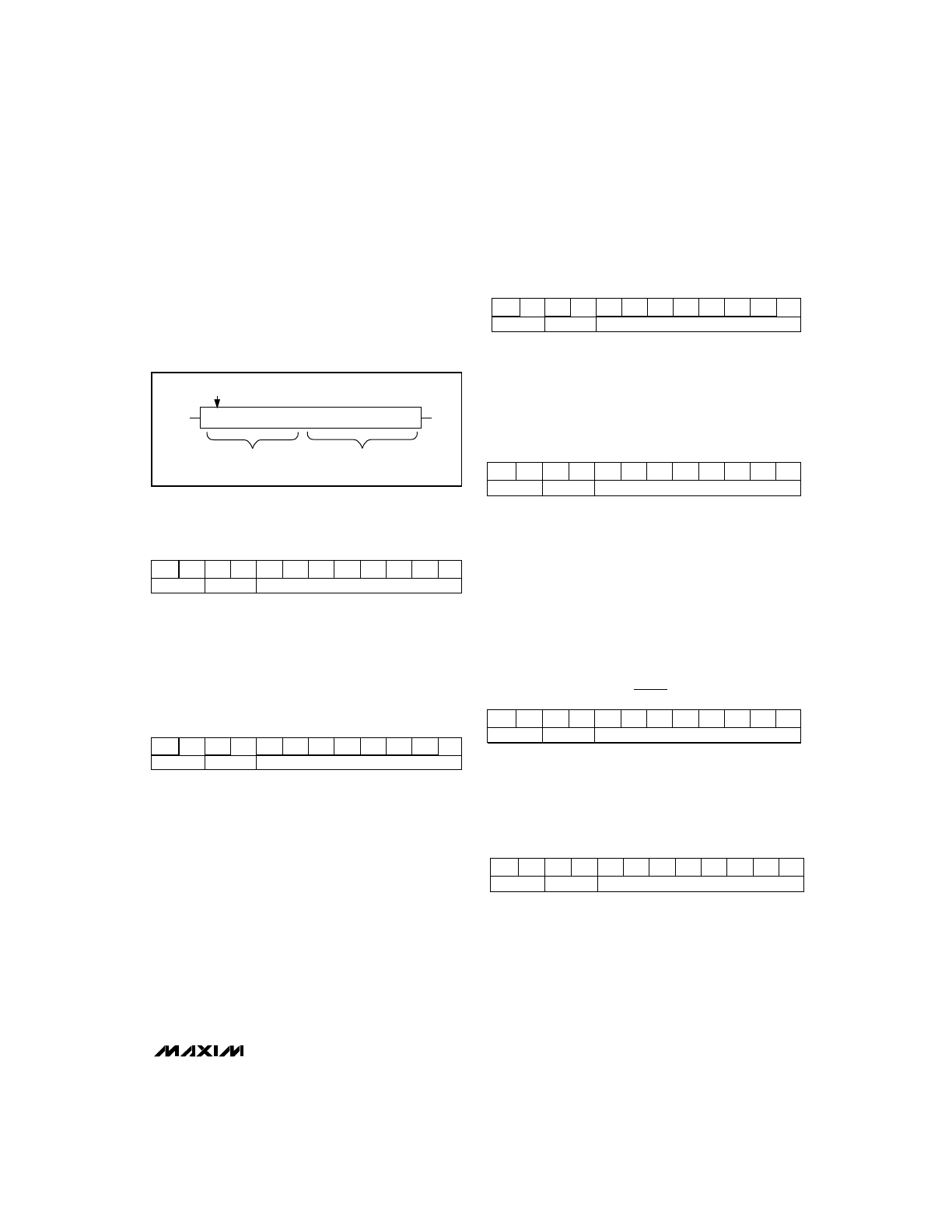
Serial Input Data Format and Control Codes
The 12-bit serial input format shown in Figure 3 com-
prises two DAC address bits (A1, A0), two control bits
(C1, C0) and eight bits of data (D0...D7).
The 4-bit address/control code configures the DAC as
shown in Table 1.
Load Input Register, DAC Registers Unchanged
(Single Update Operation)
When performing a single update operation, A1 and A0
select the respective input register. At the rising edge
of
CS, the selected input register is loaded with the cur-
rent shift-register data. All DAC outputs remain
unchanged. This preloads individual data in the input
register without changing the DAC outputs.
Load Input and DAC Registers
This command directly loads the selected DAC register
at
CS's rising edge. A1 and A0 set the DAC address.
Current shift-register data is placed in the selected
input and DAC registers.
For example, to load all four DAC registers simultaneously
with individual settings (DAC A = 1V, DAC B = 2V, DAC
C = 3V and DAC D = 4V), five commands are required.
First, perform four single input register update opera-
tions. Next, perform an “
LDAC” command as a fifth
command. All DACs will be updated from their respec-
tive input registers at the rising edge of
CS.
Update All DACs from Shift Registers
All four DAC registers are updated with shift-register
data. This command allows all DACs to be set to any
analog value within the reference range. This command
can be used to substitute
CLR if code 00 hex is pro-
grammed, which clears all DACs.
No Operation (NOP)
The NOP command (no operation) allows data to be shift-
ed through the MAX509/MAX510 shift register without
affecting the input or DAC registers. This is useful in daisy
chaining (also see the
Daisy-Chaining Devices section).
For this command, the data bits are "Don't Cares." As an
example, three MAX509/MAX510s are daisy-chained (A, B
and C), and DAC A and DAC C need to be updated. The
36-bit-wide command would consist of one 12-bit word for
device C, followed by an NOP instruction for device B and
a third 12-bit word with data for device A. At
CS's rising
edge, only device B is not updated.
“LDAC” Command (Software)
All DAC registers are updated with the contents of their
respective input registers at
CS's rising edge. With the
exception of using
CS to execute, this performs the
same function as the asynchronous
LDAC.
Set DOUT Phase – SCLK Rising (Mode 1, Default)
Mode 1 resets the serial output DOUT to transition at
SCLK's rising edge. This is the MAX509/MAX510’s
default setting after the supply voltage has been
applied.
The command also loads all DAC registers with the con-
tents of their respective input registers, and is identical to
the “
LDAC” command.
MAX509/MAX510
Quad, Serial 8-Bit DACs
with Rail-to-Rail Outputs
______________________________________________________________________________________
11
This is the first bit shifted in
A1 A0C1 C0 D7D6
● ● ●
D1 D0
DIN
DOUT
Control and
Address bits
8-bit DAC data
MSB
LSB
Figure 3. Serial Input Format
(
LDAC = H)
(
LDAC = x)
(
LDAC = x)
(
LDAC = x)
(
LDAC = x)
(
LDAC = H)
1 0
1 1
x
x
x
x
x
x
x
x
D0
D1
D2
D3
D4
D5
D6
D7
C0
C1
A0
A1
8-Bit DAC Data
0 0
x 0
D0
D1
D2
D3
D4
D5
D6
D7
C0
C1
A0
A1
x
x
x
x
x
x
x
x
0 0
x 1
D0
D1
D2
D3
D4
D5
D6
D7
C0
C1
A0
A1
1 0
0 x
x
x
x
x
x
x
x
x
D0
D1
D2
D3
D4
D5
D6
D7
C0
C1
A0
A1
8-Bit Data
0 1
Address
D0
D1
D2
D3
D4
D5
D6
D7
C0
C1
A0
A1
8-Bit Data
1 1
Address
D0
D1
D2
D3
D4
D5
D6
D7
C0
C1
A0
A1
Set DOUT Phase – SCLK Falling (Mode 0)
This command resets DOUT to transition at SCLK's falling
edge. Once this command is issued, the phase of DOUT is
latched and will not change except on power-up or if the
specific command is issued that sets the phase to rising
edge.
The same command also updates all DAC registers with
the contents of their respective input registers, identical to
the “
LDAC” command.
LDAC Operation (Hardware)
LDAC is typically used in 4-wire interfaces (Figure 7).
LDAC allows asynchronous hardware control of the DAC
outputs and is level-sensitive. With
LDAC low, the DAC reg-
isters are transparent and any time an input register is
updated, the DAC output immediately follows.
Clear DACs with CLR
Strobing the
CLR pin low causes an asynchronous clear of
input and DAC registers and sets all DAC outputs to zero.
Similar to the
LDAC pin, CLR can be invoked at any time,
typically when the device is not selected (
CS = H). When
the DAC data is all zeros, this function is equivalent to the
"Update all DACs from Shift Registers" command.
Digital Inputs and Outputs
Digital inputs and outputs are compatible with both TTL and
5V CMOS logic. The power-supply current (I
DD
) depends
on the input logic levels. Using CMOS logic to drive
CS,
SCLK, DIN,
CLR and LDAC turns off the internal level trans-
lators and minimizes supply currents.
Serial Data Output
DOUT is the output of the internal shift register. DOUT can be
programmed to clock out data on SCLK's falling edge (mode
0) or rising edge (mode 1). In mode 0, output data lags the
input data by 12.5 clock cycles, maintaining compatibility with
Microwire, SPI, and QSPI. In mode 1, output data lags the input
by 12 clock cycles. On power-up, DOUT defaults to mode 1
timing. DOUT never three-states; it always actively drives either
high or low and remains unchanged when
CS is high.
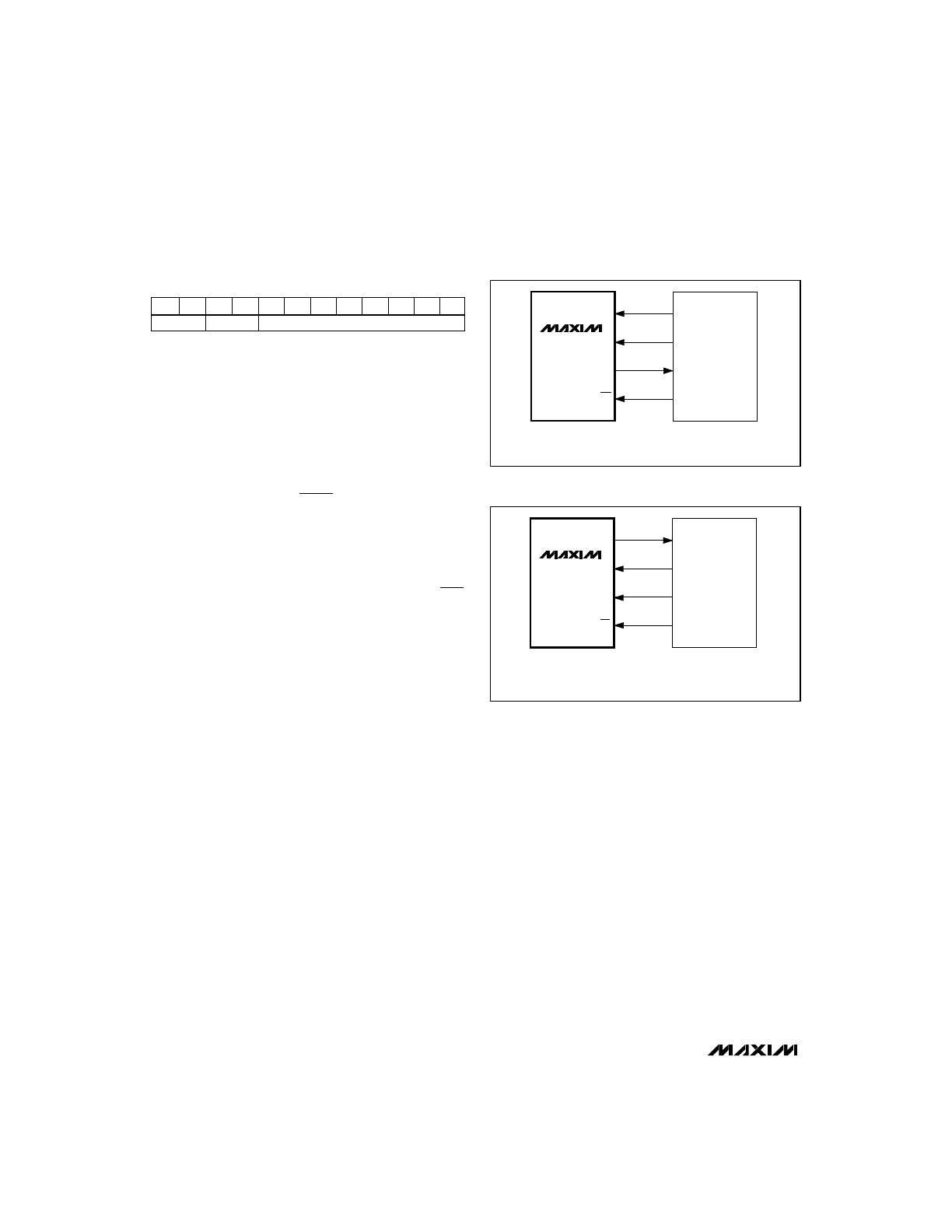
Interfacing to the Microprocessor
The MAX509/MAX510 are Microwire, SPI, and QSPI compati-
ble. For SPI and QSPI, clear the CPOL and CPHA configura-
tion bits (CPOL = CPHA = 0). The SPI/QSPI CPOL = CPHA
= 1 configuration can also be used if the DOUT output is
ignored.
The MAX509/MAX510 can interface with Intel's
80C5X/80C3X family in mode 0 if the SCLK clock polarity is
inverted. More universally, if a serial port is not available,
three lines from one of the parallel ports can be used for bit
manipulation.
Digital feedthrough at the voltage outputs is greatly mini-
mized by operating the serial clock only to update the regis-
ters. Also see the Clock Feedthrough photo in the
Typical
Operating Characteristics section. The clock idle state is low.
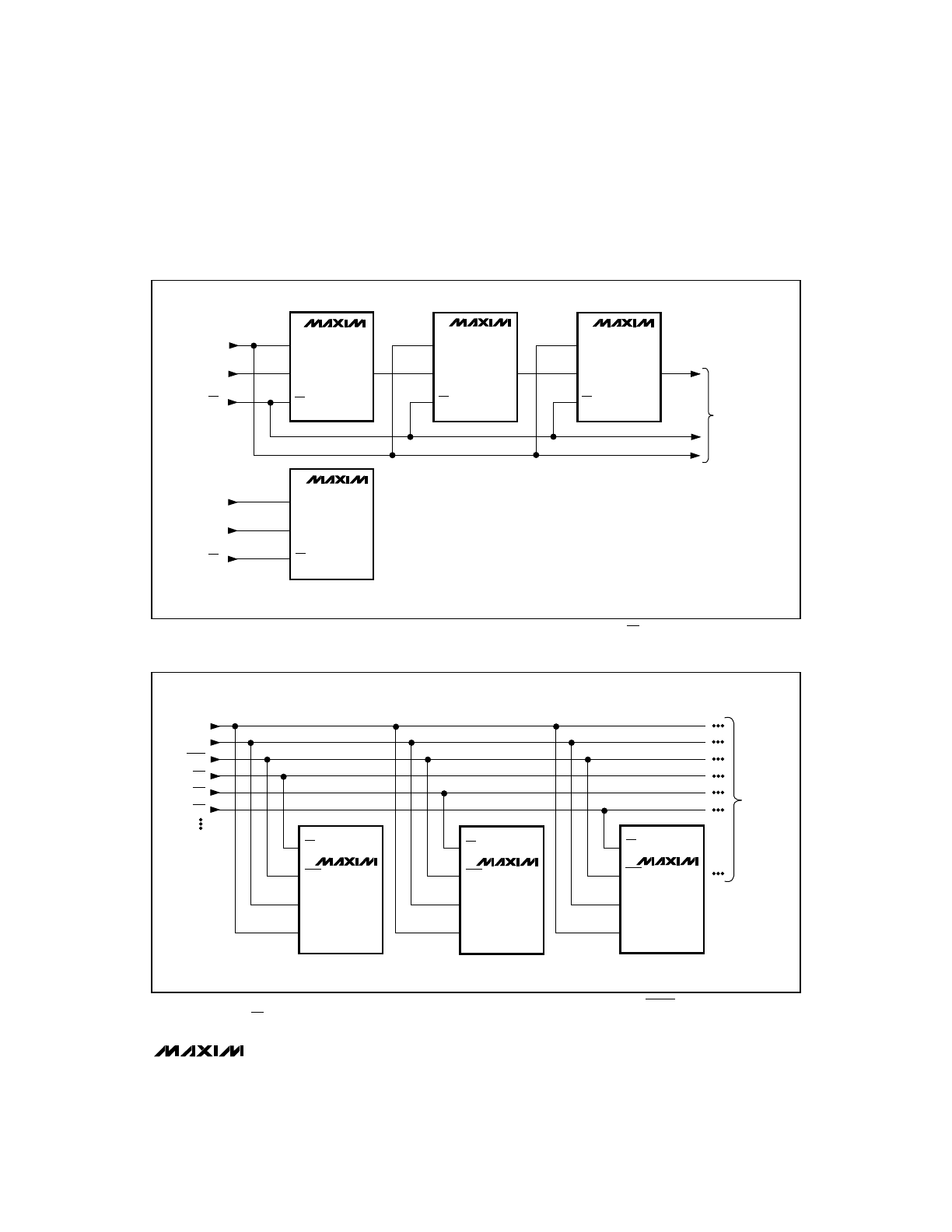
Daisy-Chaining Devices
Any number of MAX509/MAX510s can be daisy-chained by
connecting the DOUT pin of one device to the DIN pin of the
following device in the chain. The NOP instruction (Table 1)
allows data to be passed from DIN to DOUT without chang-
ing the input or DAC registers of the passing device. A three-
wire interface updates daisy-chained or individual
MAX509/MAX510s simultaneously by bringing
CS high.
Quad, Serial 8-Bit DACs
with Rail-to-Rail Outputs
12
______________________________________________________________________________________
SCLK
DIN
DOUT
CS
SK
SO
SI
I/0
MICROWIRE
PORT
MAX509
MAX510
THE DOUT-SI CONNECTION IS NOT REQUIRED FOR WRITING TO THE
MAX509/MAX510, BUT MAY BE USED FOR READ-BACK PURPOSES.
Figure 4. Connections for Microwire
DOUT
DIN
SCLK
CS
MISO
MOSI
SCK
I/0
SPI
PORT
MAX509
MAX510
THE DOUT-MISO CONNECTION IS NOT REQUIRED FOR WRITING TO THE
MAX509/MAX510, BUT MAY BE USED FOR READ-BACK PURPOSES.
CPOL = 0, CPHA = 0
Figure 5. Connections for SPI
(
LDAC = x)
A1
A0
C1
C0
D7
D6
D5
D4
D3
D2
D1
D0
x
x
x
x
x
x
x
x
1 0
1 0
MAX509/MAX510
MAX509/MAX510
Quad, Serial 8-Bit DACs
with Rail-to-Rail Outputs
______________________________________________________________________________________
13
SCLK
DIN
CS
MAX509
MAX510
SCLK
DIN
CS
MAX509
MAX510
SCLK
DIN
CS
MAX509
MAX510
SCLK
DIN
CS
MAX509
MAX510
DOUT
DOUT
DOUT
SCLK
DIN
CS
SCLK
DIN
CS
TO OTHER
SERIAL DEVICES
Figure 6. Daisy-chained or individual MAX509/MAX510s are simultaneously updated by bringing CS high. Only three wires are
required.
CS
LDAC
SCLK
DIN
MAX509
MAX510
CS
LDAC
SCLK
DIN
MAX509
MAX510
CS
LDAC
SCLK
DIN
MAX509
MAX510
TO OTHER
SERIAL
DEVICES
DIN
SCLK
LDAC
CS1
CS2
CS3
Figure 7. Multiple MAX509/MAX510 DACs sharing one DIN line. Simultaneously update by strobing LDAC, or specifically update by
enabling individual CS.
MAX509/MAX510
Quad, Serial 8-Bit DACs
with Rail-to-Rail Outputs
14
______________________________________________________________________________________
If multiple devices share a common DIN line, Figure 7's
configuration provides simultaneous update by strob-
ing
LDAC low. CS1, CS2, CS3... are driven separately,
thus controlling which data are written to devices 1, 2, 3....
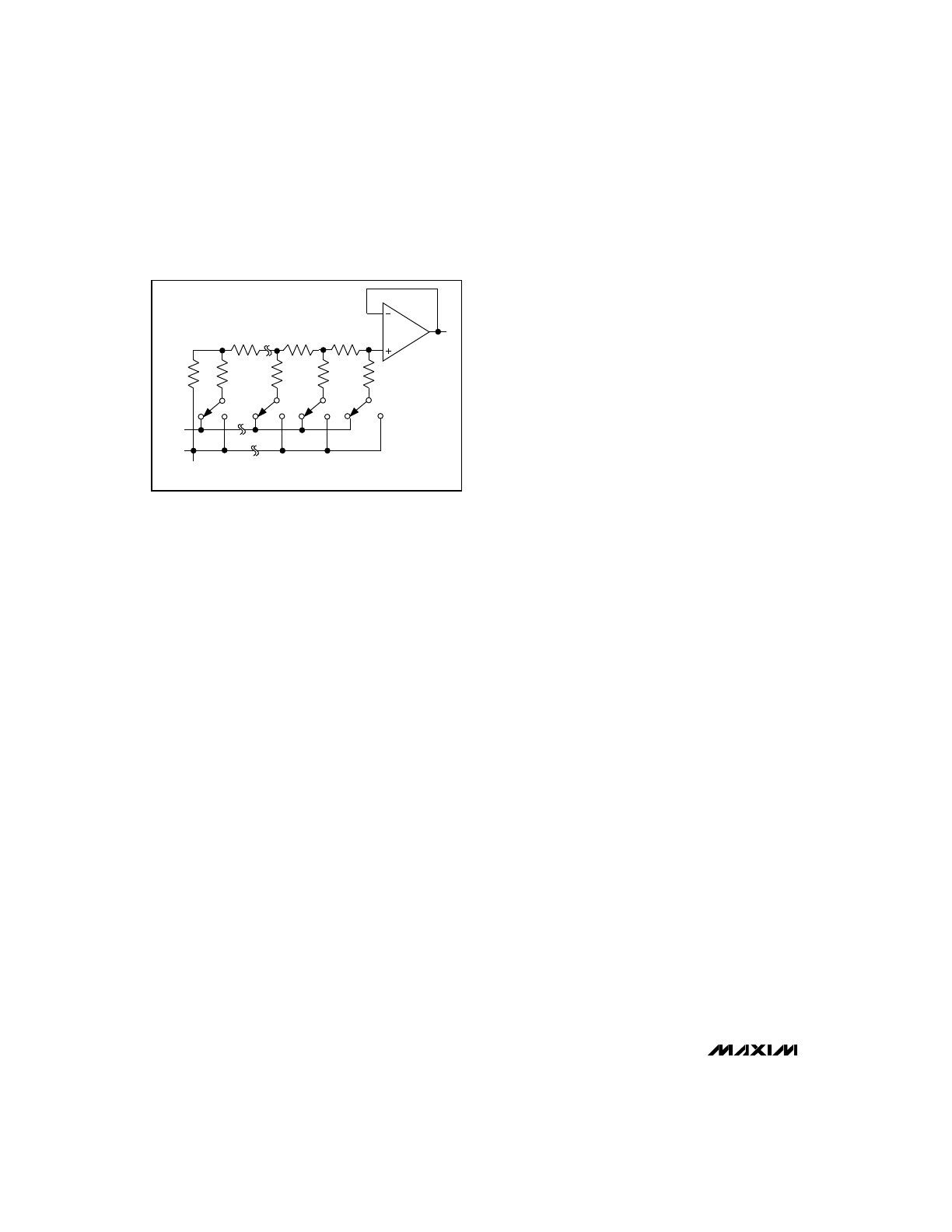
Analog Section
DAC Operation
The MAX509/MAX510 contain four matched voltage-
output DACs. The DACs are inverted R-2R ladder net-
works that convert 8-bit digital words into equivalent
analog output voltages in proportion to the applied ref-
erence voltages. Each DAC in the MAX509 has a sepa-
rate reference input, while the two reference inputs in
the MAX510 each share a pair of DACs. The two refer-
ence inputs permit different full-scale output voltage
ranges for each pair of DACs. A simplified diagram of
one of the four DACs is shown in Figure 8.
Reference Input
The MAX509/MAX510 can be used for multiplying
applications. The reference accepts both DC and AC
signals. The voltage at each REF input sets the full-
scale output voltage for its respective DAC(s). If the ref-
erence voltage is positive, both the MAX509 and
MAX510 can be operated from a single supply. If dual
supplies are used, the reference input can vary from
V
SS
to V
DD
, but is always referred to AGND. The input
impedance at REF is code dependent, with the lowest
value (16k
Ω
for the MAX509 and 8k
Ω
for the MAX510)
occurring when the input code is 55 hex or 0101 0101.
The maximum value, practically infinity, occurs when
the input code is 00 hex. Since the REF input imped-
ance is code dependent, the DAC's reference sources
must have a low output impedance (no more than 32
Ω
for the MAX509 and 16
Ω
for the MAX510) to maintain
output linearity. The REF input capacitance is also code
dependent: 15pF typical for the MAX509 and 30pF
typical for the MAX510.
The output voltage for any DAC can be represented by
a digitally programmable voltage source as:
VOUT = (NB x VREF) / 256
where NB is the numerical value of the DAC's binary
input code.
Output Buffer Amplifiers
All MAX509/MAX510 voltage outputs are internally
buffered by precision unity-gain followers that slew at
up to 1V/µs. The outputs can swing from V
SS
to V
DD
.
With a 0V to +4V (or +4V to 0V) output transition, the
amplifier outputs will settle to 1/2LSB in typically 6µs
when loaded with 10k
Ω
in parallel with 100pF.
The buffer amplifiers are stable with any combination of
resistive loads
≥
2k
Ω
and capacitive loads
≤
300pF.
__________Applications Information
Power Supply and
Reference Operating Ranges
The MAX509/MAX510 are fully specified to operate with
V
DD
= 5V ±10% and V
SS
= 0V to -5.5V. 8-bit perfor-
mance is guaranteed for both single- and dual-supply
operation. The zero-code output error is less than 14mV
when operating from a single +5V supply.
The DACs work well with reference voltages from V
SS
to V
DD
. The reference voltage is referred to AGND.
The preferred power-up sequence is to apply V
SS
and
then V
DD
, but bringing up both supplies at the same
time is also acceptable. In either case, the voltage
applied to REF should not exceed V
DD
during power-
up or at any other time. If proper power sequencing is
not possible, connect an external Schottky diode
between V
SS
and AGND to ensure compliance with the
Absolute Maximum Ratings. Do not apply signals to
the digital inputs before the device is fully powered up.
Power-Supply Bypassing
and Ground Management
In single-supply operation (AGND = DGND = V
SS
=
0V), AGND, DGND and V
SS
should be connected
together in a "star" ground at the chip. This ground
should then return to the highest quality ground avail-
able. Bypass V
DD
with a 0.1µF capacitor, located as
close to V
DD
and DGND as possible. In dual-supply
operation, bypass V
SS
to AGND with 0.1µF.
Careful PC board layout minimizes crosstalk among
DAC outputs, reference inputs, and digital inputs.
Figures 9 and 10 show suggested circuit board layouts
to minimize crosstalk.
2R
R
R
R
2R
2R
2R
2R
2R
D0
D5
D6
D7
REF_
AGND
SHOWN FOR ALL 1 ON DAC
OUT_
Figure 8. DAC Simplified Circuit Diagram
MAX509/MAX510
Quad, Serial 8-Bit DACs
with Rail-to-Rail Outputs
______________________________________________________________________________________
15
Unipolar-Output, 2-Quadrant Multiplication
In unipolar operation, the output voltages and the refer-
ence input(s) are the same polarity. Figures 11 and 12
show the MAX509/MAX510 unipolar configurations.
Both devices can be operated from a single supply if
the reference inputs are positive. If dual supplies are
used, the reference input can vary from V
SS
to V
DD
.
Table 2 shows the unipolar code.
Bipolar-Output, 2-Quadrant Multiplication
Bipolar-output, 2-quadrant multiplication is achieved by
offsetting AGND positively or negatively. Table 3 shows
the bipolar code.
AGND can be biased above DGND to provide an arbi-
trary nonzero output voltage for a 0 input code, as
shown in Figure 13. The output voltage at OUTA is:
V
OUTA
= V
BIAS
+ (NB/256)(V
IN
),
Figure 9. Suggested MAX509 PC Board Layout for Minimizing
Crosstalk (Bottom View)
OUTC
OUTD
V
DD
REFC
REFD
OUTB
OUTA
V
SS
REFB
REFA
SYSTEM GND
AGND
Figure 10. Suggested MAX510 PC Board Layout for Minimizing
Crosstalk (Bottom View)
OUTC
OUTD
V
DD
REFCD
OUTB
OUTA
V
SS
REFAB
SYSTEM GND
AGND
DAC CONTENTS
MSB
LSB
ANALOG
OUTPUT
1 1 1 1
1 1 1 1
255
+V
REF
(
––––
)
256
1 0 0 0
0 0 0 1
129
+V
REF
(
––––
)
256
1 0 0 0
0 0 0 0
128 V
REF
+V
REF
(
––––
)
= + –
–––
256 2
0 1 1 1
1 1 1 1
127
+V
REF
(
––––
)
256
0 0 0 0
0 0 0 0
0V
0 0 0 0
0 0 0 1
1
+V
REF
(
––––
)
256
Table 2. Unipolar Code Table
1
Note:
1LSB = (V
REF
) (2-8) = +V
REF
(
––––
)
256
Table 3. Bipolar Code Table
1 0 0 0
DAC CONTENTS
0 0 0 1
MSB
LSB
ANALOG
OUTPUT
1 1 1 1
1 1 1 1
127
+V
REF
(
––––
)
128
1
+V
REF
(
––––
)
128
1 0 0 0
0 0 0 0
0V
0 1 1 1
1 1 1 1
1
-V
REF
(
––––
)
128
0 0 0 0
0 0 0 0
128
-V
REF
(
––––
)
= -V
REF
128
0 0 0 0
0 0 0 1
127
-V
REF
(
––––
)
128
MAX509/MAX510
where NB represents the digital input word. Since
AGND is common to all four DACs, all outputs will be
offset by V
BIAS
in the same manner. Do not bias AGND
more than +1V above DGND, or more than 2.5V below
DGND.
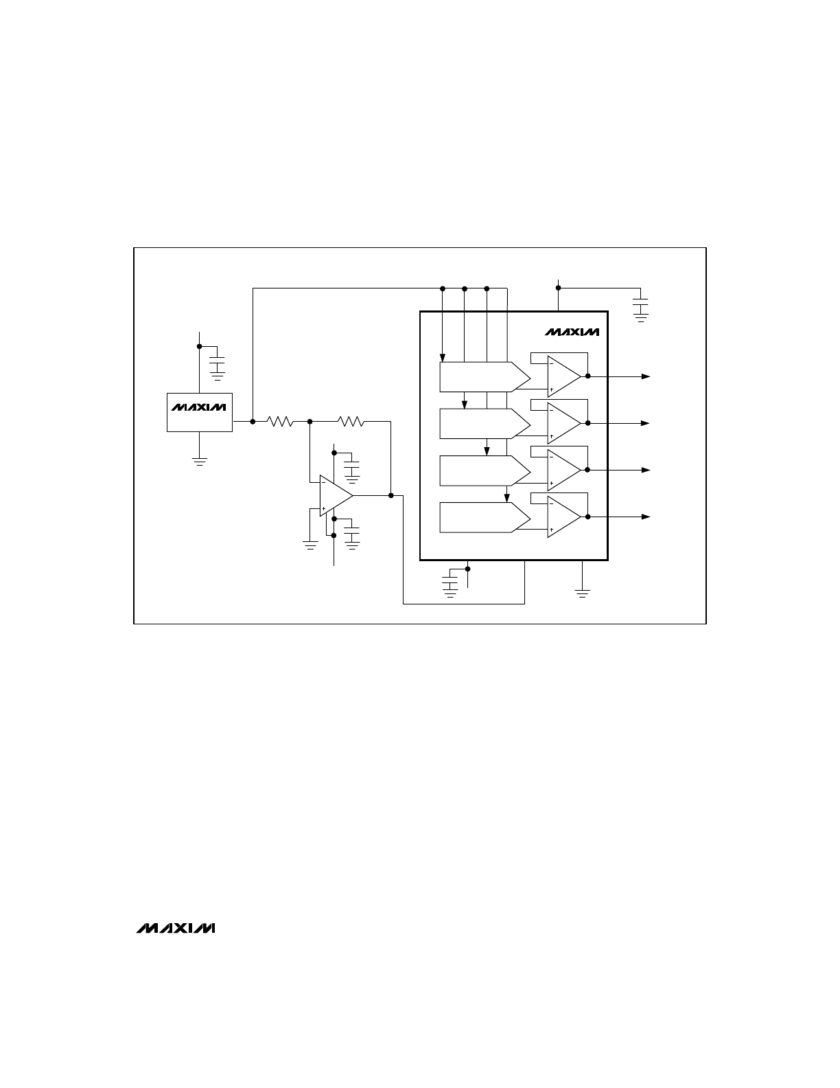
Figures 14 and 15 illustrate the generation of negative
offsets with bipolar outputs. In these circuits, AGND is
biased negatively (up to -2.5V with respect to DGND) to
provide an arbitrary negative output voltage for a 0
input code. The output voltage at OUTA is:
OUTA = -(R2/R1)(2.5V) + (NB/256)(2.5V)(R2/R1+1)
where NB represents the digital input word. Since
AGND is common to all four DACs, all outputs will be
offset by V
BIAS
in the same manner. Table 3, with
V
REF
= 2.5V, shows the digital code vs. output voltage
for Figure 14 and 15's circuits with R1 = R2. The
ICL7612 op amp is chosen because its common-mode
range extends to both supply rails.
Quad, Serial 8-Bit DACs
with Rail-to-Rail Outputs
16
______________________________________________________________________________________
Figure 11. MAX509 Unipolar Output Circuit
REFD
DAC A
DAC B
DAC C
DAC D
REFC
REFB
REFA
MAX509
OUTA
OUTB
OUTC
OUTD
SERIAL
INTERFACE
NOT SHOWN
REFERENCE INPUTS (V
SS
TO V
DD
)
2
1
20
19
V
DD
+5V
16
5
17
4
18
3
-5V (OR GND)
6
8
V
SS
AGND
DGND
Figure 12. MAX510 Unipolar Output Circuit
DAC A
DAC B
DAC C
DAC D
REFAB
MAX510
OUTA
OUTB
OUTC
OUTD
SERIAL
INTERFACE
NOT SHOWN
REFERENCE INPUTS (V
SS
TO V
DD
)
2
1
16
15
V
DD
+5V
4
14
3
-5V (OR GND)
5
6
V
SS
AGND
DGND
REFCD
13
Figure 13. MAX509/MAX510 AGND Bias Circuits (Positive
Offset)
DAC A
MAX509
5
18
AGND
2
OUTA
DGND
V
SS
REFA
V
DD
3
8
V
IN
V
BIAS
6
+5V
-5V (OR GND)
DAC A
MAX510
4
14
AGND
2
OUTA
DGND
V
SS
REFAB
V
DD
3
6
V
IN
V
BIAS
5
+5V
-5V (OR GND)
SERIAL INTERFACE NOT SHOWN
MAX509/MAX510
Quad, Serial 8-Bit DACs
with Rail-to-Rail Outputs
______________________________________________________________________________________
17
Figure 14. MAX509 AGND Bias Circuit (Negative Offset)
DAC A
DAC B
DAC C
DAC D
MAX509
OUTA
OUTB
OUTC
OUTD
SERIAL
INTERFACE
NOT SHOWN
REFERENCE INPUTS
2
1
20
19
V
DD
+5V
16
5
17
4
18
3
-5V
8
V
SS
AGND
DGND
6
0.1
µ
F
0.1
µ
F
MAX873
+5V
0.1
µ
F
R1
330k
0.1%
+5V
+2.5V
0.1
µ
F
0.1
µ
F
-5V
6
8
7
2
3
1
R2
330k
0.1%
ICL7611A
4-Quadrant Multiplication
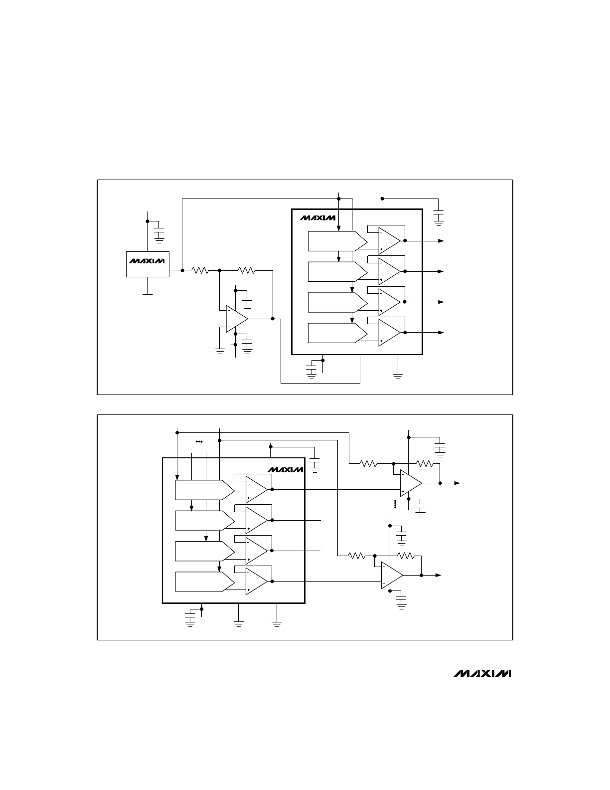
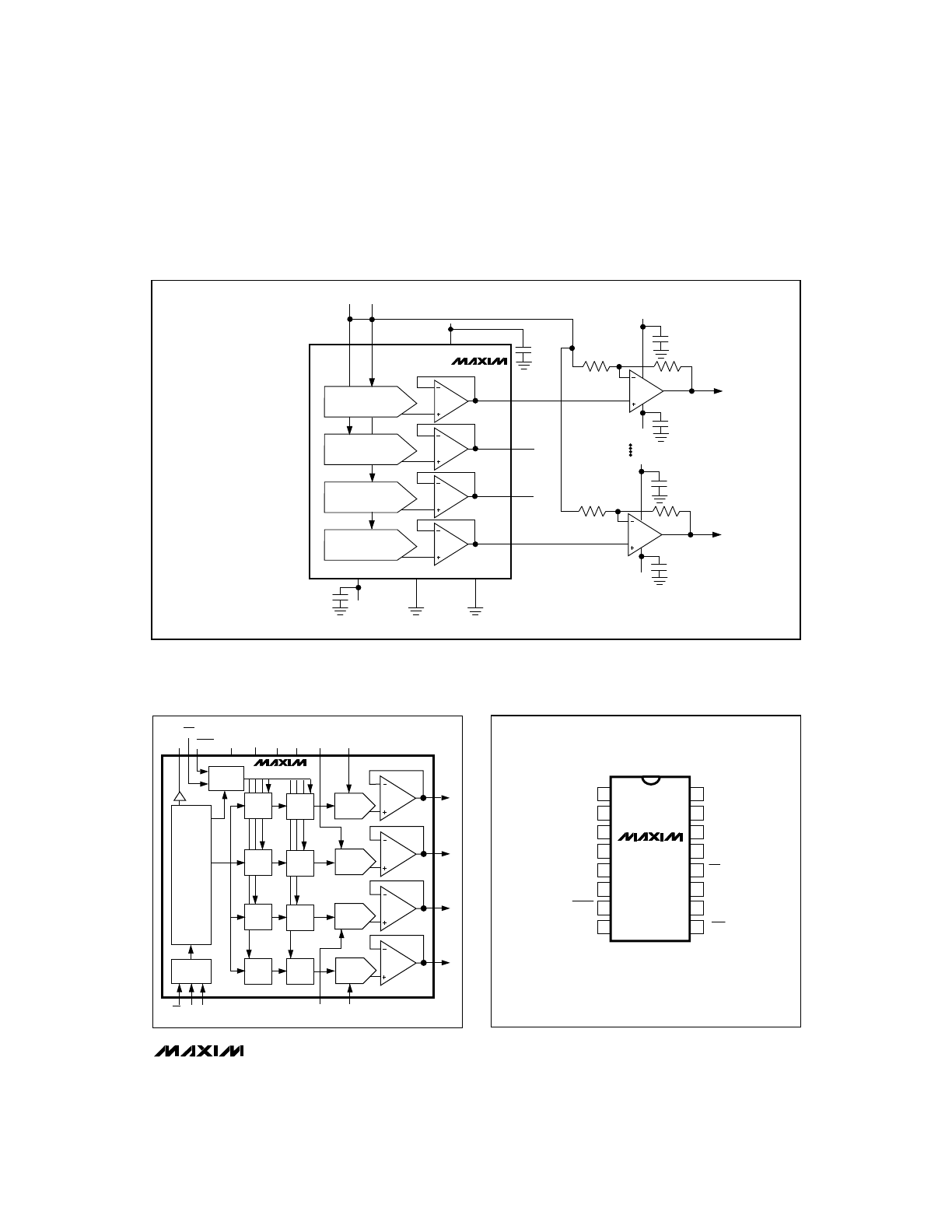
Each DAC output may be configured for 4-quadrant
multiplication using Figure 16 and 17's circuit. One op
amp and two resistors are required per channel. With
R1 = R2:
V
OUT
= V
REF
[2(NB/256)-1]
where NB represents the digital word in DAC register A.
The recommended value for resistors R1 and R2 is
330k
Ω
(±0.1%). Table 3 shows the digital code vs. out-
put voltage for Figure 16 and 17's circuit.
MAX509/MAX510
Quad, Serial 8-Bit DACs
with Rail-to-Rail Outputs
18
______________________________________________________________________________________
Figure 15. MAX510 AGND Bias Circuit (Negative Offset)
DAC A
DAC B
DAC C
DAC D
MAX510
OUTA
OUTB
OUTC
OUTD
SERIAL
INTERFACE
NOT SHOWN
REFERENCE INPUTS
2
1
16
15
V
DD
+5V
13
4
14
3
-5V
6
V
SS
AGND
DGND
5
0.1
µ
F
0.1
µ
F
MAX873
+5V
0.1
µ
F
R1
330k
0.1%
+5V
+2.5V
0.1
µ
F
0.1
µ
F
-5V
6
8
7
2
3
1
R2
330k
0.1%
ICL7611A
6
4
2
DAC A
DAC B
DAC C
DAC D
MAX509
OUTA
OUTB
OUTC
OUTD
SERIAL
INTERFACE
NOT SHOWN
REFERENCE INPUTS (V
SS
TO V
DD
)
2
1
20
19
V
DD
+5V
16
5
17
4
18
3
AGND OR -5V
8
V
SS
AGND
DGND
6
*CONNECT ICL7612A PIN 8 TO AGND
+5V
0.1
µ
F
0.1
µ
F
R1
0.1
µ
F
R2
-5V
V
OUT
+5V
R1
R2
0.1
µ
F
V
OUT
0.1
µ
F
-5V
0.1
µ
F
ICL7612A*
ICL7612A*
Figure 16. MAX509 Bipolar Output Circuit
MAX509/MAX510
Quad, Serial 8-Bit DACs
with Rail-to-Rail Outputs
______________________________________________________________________________________
19
DAC A
DAC B
DAC C
DAC D
MAX510
OUTA
OUTB
OUTC
OUTD
SERIAL
INTERFACE
NOT SHOWN
REFERENCE INPUTS
2
1
16
15
V
DD
+5V
13
4
14
3
AGND OR -5V
6
V
SS
AGND
DGND
5
*CONNECT ICL7612A PIN 8 TO AGND
+5V
0.1
µ
F
0.1
µ
F
R1
0.1
µ
F
R2
-5V
V
OUT
+5V
R1
R2
0.1
µ
F
V
OUT
0.1
µ
F
-5V
0.1
µ
F
ICL7612A*
ICL7612A*
Figure 17. MAX510 Bipolar Output Circuit
TOP VIEW
16
15
14
13
12
11
10
9
1
2
3
4
5
6
7
8
OUTC
OUTD
V
DD
REFCD
REFAB
V
SS
OUTA
OUTB
MAX510
CS
SCLK
DIN
CLR
DOUT
LDAC
DGND
AGND
DIP/Wide SO
____Pin Configurations (continued)
MAX509
OUTA
DAC A
DAC B
DAC C
DAC D
REFA
REFB
DAC
REG A
DECODE
CONTROL
INPUT
REG A
DAC
REG B
INPUT
REG B
DAC
REG C
INPUT
REG C
DAC
REG D
INPUT
REG D
12-BIT
SHIFT
REGISTER
SR
CONTROL
CS DIN SCLK
REFC
REFD
OUTB
OUTC
OUTD
DOUT
LDAC
CLR
V
DD
DGND V
SS
AGND
__Functional Diagrams (continued)
Maxim cannot assume responsibility for use of any circuitry other than circuitry entirely embodied in a Maxim product. No circuit patent licenses are
implied. Maxim reserves the right to change the circuitry and specifications without notice at any time.
20
__________________Maxim Integrated Products, 120 San Gabriel Drive, Sunnyvale, CA 94086 (408) 737-7600
© 1996 Maxim Integrated Products
Printed USA
is a registered trademark of Maxim Integrated Products.
MAX509/MAX510
Quad, Serial 8-Bit DACs
with Rail-to-Rail Outputs
___________________Chip Topography
_Ordering Information (continued)
PART
TEMP. RANGE
PIN-PACKAGE
MAX509AEPP
-40°C to +85°C
20 Plastic DIP
MAX509BEPP
-40°C to +85°C
20 Plastic DIP
MAX509AEWP
-40°C to +85°C
20 Wide SO
±1
±1 1/2
±1
MAX509BEWP
-40°C to +85°C
20 Wide SO
±1 1/2
MAX509AEAP
-40°C to +85°C
20 SSOP
±1
MAX509BEAP
-40°C to +85°C
20 SSOP
±1 1/2
MAX509AMJP
-55°C to +125°C
20 CERDIP**
±1
MAX509BMJP
-55°C to +125°C
20 CERDIP**
±1 1/2
MAX510
ACPE
16 Plastic DIP
±1
MAX510BCPE
0°C to +70°C
16 Plastic DIP
±1 1/2
MAX510ACWE
0°C to +70°C
16 Wide SO
±1
MAX510BCWE
0°C to +70°C
16 Wide SO
±1 1/2
MAX510AEPE
-40°C to +85°C
16 Plastic DIP
±1
MAX510BEPE
-40°C to +85°C
16 Plastic DIP
±1 1/2
MAX510AEWE
-40°C to +85°C
16 Wide SO
±1
MAX510BEWE
-40°C to +85°C
16 Wide SO
±1 1/2
0°C to +70°C
MAX510AMJE
-55°C to +125°C
16 CERDIP**
±1
MAX510BMJE
-55°C to +125°C
16 CERDIP**
±1 1/2
**Contact factory for availability and processing to MIL-STD-883.
________________________________________________________Package Information
L
DIM
A
A1
B
C
D
E
e
H
L
α
MIN
0.068
0.002
0.010
0.005
0.278
0.205
0.301
0.022
0˚
MAX
0.078
0.008
0.015
0.009
0.289
0.212
0.311
0.037
8˚
MIN
1.73
0.05
0.25
0.13
7.07
5.20
7.65
0.55
0˚
MAX
1.99
0.21
0.38
0.22
7.33
5.38
7.90
0.95
8˚
INCHES
MILLIMETERS
α
20-PIN PLASTIC
SHRINK
SMALL-OUTLINE
PACKAGE
H
E
D
A
A1
C
0.127mm
0.004in.
B
0.65 BSC
0.0256 BSC
21-0003A
e
REFC
(REFCD)
SCLK
CS
REFB
(REFAB)
AGND
V
SS
OUTC
OUTD
V
DD
CLR
DOUT
LDAC
0.121"
(3.07mm)
0.128"
(3.25mm)
DGND
REFA
(REFAB)
DIN
REFD
(REFCD)
OUTA
OUTB
MAX509/MAX510
NOTE:
LABELS IN ( ) ARE FOR MAX510 ONLY.
TRANSISTOR COUNT: 2235;
SUBSTRATE CONNECTED TO VDD.
TUE
(LSB)