
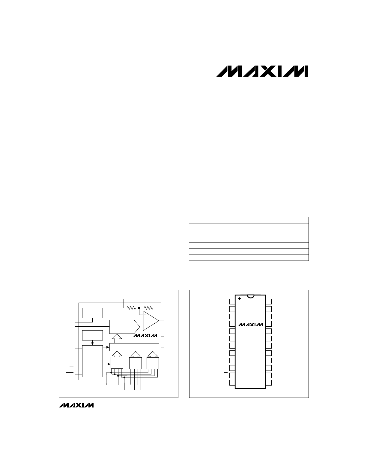
_______________General Description
The MAX503 is a low-power, 10-bit, voltage-output digital-
to-analog converter (DAC) that uses single 5V or dual ±5V
supplies. This device has an internal voltage reference plus
an output buffer amplifier. Operating current is only 250µA
from a single 5V supply, making it ideal for portable and
battery-powered applications. In addition, the shrink small-
outline package (SSOP) measures only 0.1 square inches,
using less board area than an 8-pin DIP. 10-bit resolution is
achieved through laser trimming of the DAC, op amp, and
reference. No further adjustments are necessary.
Internal gain-setting resistors can be used to define a DAC
output voltage range of 0V to +2.048V, 0V to +4.096V, or
±2.048V. Four-quadrant multiplication is possible without
the use of external resistors or op amps. The parallel logic
inputs are double buffered and are compatible with 4-bit, 8-
bit, and 16-bit microprocessors. For a hardware and soft-
ware compatible 12-bit upgrade, refer to the MAX530 data
sheet. For DACs with similar features but with a serial data
interface, refer to the MAX504/MAX515 data sheet.
________________________Applications
Battery-Powered Data-Conversion Products
Minimum Component-Count Analog Systems
Digital Offset/Gain Adjustment
Industrial Process Control
Arbitrary Function Generators
Automatic Test Equipment
Microprocessor-Controlled Calibration
____________________________Features
♦
Buffered Voltage Output
♦
Internal 2.048V Voltage Reference
♦
Operates from Single 5V or Dual ±5V Supplies
♦
Low Power Consumption:
250µA Operating Current
40µA Shutdown-Mode Current
♦
SSOP Package Saves Space
♦
Relative Accuracy: ±
1
/
2
LSB Max Over
Temperature
♦
Guaranteed Monotonic Over Temperature
♦
4-Quadrant Multiplication with No External
Components
♦
Power-On Reset
♦
Double-Buffered Parallel Logic Inputs
______________Ordering Information
MAX503
5V, Low-Power, Parallel-Input,
Voltage-Output, 10-Bit DAC
________________________________________________________________
Maxim Integrated Products
1
24
23
22
21
20
19
18
17
1
2
3
4
5
6
7
8
D6/S0
V
DD
ROFS
RFB
D2
D9/D1
D8/D0
D7/S1
TOP VIEW
VOUT
V
SS
REFOUT
REFGND
A0
D5
D4
D3
16
15
14
13
9
10
11
12
LDAC
CLR
AGND
REFIN
DGND
CS
WR
A1
DIP/SO/SSOP
MAX503
__________________Pin Configuration
MAX503
REFOUT
REFIN ROFS
2.048V
REFERENCE
POWER-ON
RESET
DAC
CONTROL
LOGIC
REFGND
AGND
CLR
A0
A1
CS
WR
LDAC
V
DD
DGND
V
SS
VOUT
RFB
17
14
DAC LATCH
NBL
INPUT
LATCH
D6/S0
D7/S1
D8/D0
D2
D9/D1
D4
D3
D5
NBM
INPUT
LATCH
NBH
INPUT
LATCH
24
1
2
3
4 5 6 7
21
20
23
12
19
18
13
22
15
8
9
11
10
16
10-BIT DAC LATCH
________________Functional Diagram
Call toll free 1-800-998-8800 for free samples or literature.
PART
TEMP. RANGE
PIN-PACKAGE
MAX503CNG
0°C to +70°C
24 Narrow Plastic DIP
MAX503CWG
0°C to +70°C
24 Wide SO
MAX503CAG
0°C to +70°C
24 SSOP
19-0279; Rev 0; 8/94
Refer to the MAX530 for military temperature or die equivalents.
MAX503ENG
-40°C to +85°C
24 Narrow Plastic DIP
MAX503EWG
-40°C to +85°C
24 Wide SO
MAX503EAG
-40°C to +85°C
24 SSOP
MAX503
5V, Low-Power, Parallel-Input,
Voltage-Output, 10-Bit DAC
2
_______________________________________________________________________________________
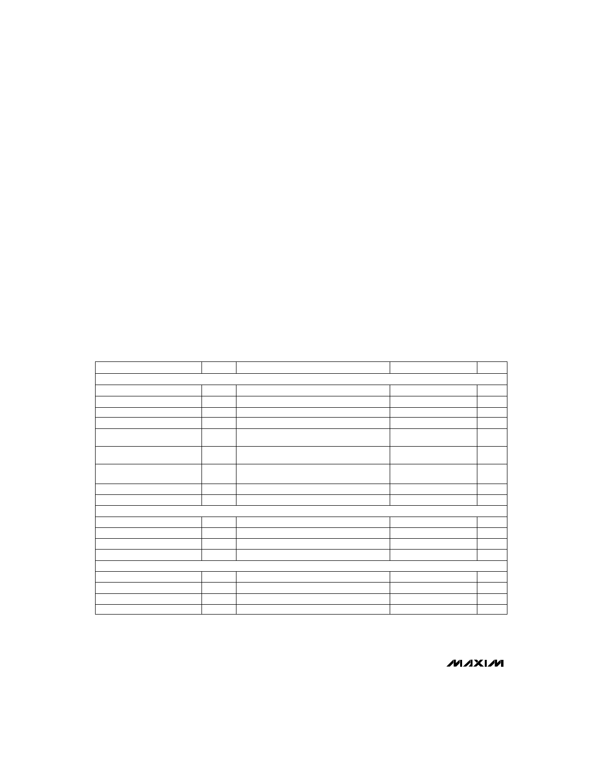
ABSOLUTE MAXIMUM RATINGS
V
DD
to DGND and V
DD
to AGND ................................-0.3V, +6V
V
SS
to DGND and V
SS
to AGND .................................-6V, +0.3V
V
DD
to V
SS
............................................................... -0.3V, +12V
AGND to DGND........................................................-0.3V, +0.3V
REFGND to AGND.........................................-0.3V, (V
DD
+ 0.3V)
Digital Input Voltage to DGND .................... -0.3V, (V
DD
+ 0.3V)
REFIN ..................................................(V
SS
- 0.3V), (V
DD
+ 0.3V)
REFOUT ..............................................(V
SS
- 0.3V), (V
DD
+ 0.3V)
REFOUT to REFGND .................................... -0.3V, (V
DD
+ 0.3V)
RFB ....................................................(V
SS
- 0.3V), (V
DD
+ 0.3V)
ROFS ..................................................(V
SS
- 0.3V), (V
DD
+ 0.3V)
VOUT to AGND (Note 1) .............................................. V
SS,
V
DD
Continuous Current, Any Input ........................................±20mA
Continuous Power Dissipation (T
A
= +70°C)
Narrow Plastic DIP (derate 13.33mW/°C above +70°C) ...1067mW
Wide SO (derate 11.76mW/°C above +70°C)............... 941mW
SSOP (derate 8.00mW/°C above +70°C) ......................640mW
Operating Temperature Ranges
MAX503C_G .........................................................0°C to +70°C
MAX503E_G ......................................................-40°C to +85°C
Storage Temperature Range .............................-65°C to +165°C
Lead Temperature (soldering, 10sec) ........................... +300°C
Stresses beyond those listed under “Absolute Maximum Ratings” may cause permanent damage to the device. These are stress ratings only, and functional
operation of the device at these or any other conditions beyond those indicated in the operational sections of the specifications is not implied. Exposure to
absolute maximum rating conditions for extended periods may affect device reliability.
PARAMETER
SYMBOL
MIN
TYP
MAX
UNITS
Differential Nonlinearity
DNL
±1
LSB
Unipolar Offset Error
V
OS
0
0.25
3
LSB
Unipolar Offset
Temperature Coefficient
TCV
OS
3
ppm/°C
Unipolar Offset-Error
Supply Rejection
PSRR
0.1
LSB/V
Resolution
STATIC PERFORMANCE
N
10
Bits
Gain-Error Temperature Coefficient
1
ppm/°C
Gain-Error Power-Supply Rejection
PSRR
0.1
LSB/V
DAC VOLTAGE OUTPUT (VOUT)
Output Voltage Range
0
V
DD
- 0.4
V
Resistive Load
2
k
Ω
DC Output Impedance
0.2
Ω
Short-Circuit Current
I
SC
12
mA
REFERENCE INPUT (REFIN)
Reference Input Range
0
V
DD
- 2
V
Reference Input Resistance
40
k
Ω
Reference Input Capacitance
10
50
pF
AC Feedthrough
-80
dB
CONDITIONS
Guaranteed monotonic
4.5V
≤
V
DD
≤
5.5V
4.5V
≤
V
DD
≤
5.5V
VOUT = 2V, load regulation
≤
±0.5LSB
Code dependent, minimum at code 0101...
Code dependent (Note 3)
(Note 4)
Gain Error (Note 2)
GE
LSB
±1
Note 1:
The output may be shorted to V
DD
, V
SS
, DGND, or AGND if the continuous package power dissipation and current ratings
are not exceeded. Typical short-circuit currents are 20mA.
ELECTRICAL CHARACTERISTICS—Single +5V Supply
(V
DD
= 5V, V
SS
= 0V, AGND = DGND = REFGND = 0V, REFIN = 2.048V (external), RFB = ROFS = VOUT, C
REFOUT
= 33µF,
R
L
= 10k
Ω
, C
L
= 100pF, TA = TMIN to TMAX, unless otherwise noted.)
DAC latch = all 1s,
VOUT < V
DD
- 0.4V (Note 2)
Relative Accuracy
INL
±0.5
LSB
(Note 2)
MAX503
5V, Low-Power, Parallel-Input,
Voltage-Output, 10-Bit DAC
_______________________________________________________________________________________
3
ELECTRICAL CHARACTERISTICS—Single +5V Supply (continued)
(V
DD
= 5V, V
SS
= 0V, AGND = DGND = REFGND = 0V, REFIN = 2.048V (external), RFB = ROFS = VOUT, C
REFOUT
= 33µF,
R
L
= 10k
Ω
, C
L
= 100pF, TA = TMIN to TMAX, unless otherwise noted.)
PARAMETER
Temperature Coefficient
SYMBOL
MIN
TYP
MAX
UNITS
Reference Tolerance
V
REFOUT
ppm/°C
2.011
2.085
DYNAMIC PERFORMANCE
V
2.015
2.081
REFERENCE OUTPUT (REFOUT)
Voltage Output Slew Rate
Reference Output Resistance
R
REFOUT
2
Ω
Power-Supply Rejection Ratio
PSRR
200
µV/V
0.15
0.25
V/µs
Voltage Output Settling Time
Noise Voltage
e
n
400
25
µVp-p
µs
30
Digital Feedthrough
5
nV-s
68
Signal-to-Noise Plus
Distortion Ratio
SINAD
68
dB
DIGITAL INPUTS (S0, S1, D0–D9, LDAC, CLR, CS, WR, A0, A1)
Logic High Input
V
IH
2.4
V
Logic Low Input
V
IL
0.8
V
Digital Leakage Current
±1
µA
Digital Input Capacitance
8
pF
POWER SUPPLIES
CONDITIONS
(Note 5)
4.5V
≤
V
DD
≤
5.5V
T
A
= +25°C
To ±0.5LSB, VOUT = 2V
WR = V
DD
, digital inputs all 1s to all 0s
Unity gain (Note 4)
Gain = 2 (Note 4)
V
IN
= 0V or V
DD
2.024
2.048
2.072
T
A
= +25°C
0.1Hz to 10kHz
Positive Supply-Voltage Range
V
DD
4.5
5.5
V
Positive Supply Current
I
DD
Outputs unloaded, all digital inputs = 0V or V
DD
250
400
µA
SWITCHING CHARACTERISTICS
Address to WR Setup
t
AWS
5
ns
Address to WR Hold
t
AWH
5
ns
CS to WR Setup
t
CWS
0
ns
CS to WR Hold
t
CWH
0
ns
Data to WR Setup
t
DS
45
ns
Data to WR Hold
t
DH
0
ns
WR Pulse Width
t
WR
45
ns
LDAC Pulse Width
t
LDAC
45
ns
CLR Pulse Width
t
CLR
45
ns
Internal Power-On Reset
Pulse Width
t
POR
(Note 3)
1.3
10
µs
Required External Capacitor
C
REFOUT
3.3
µF
MAX503E
MAX503C
ELECTRICAL CHARACTERISTICS—Dual ±5V Supplies
(V
DD
= 5V, V
SS
= -5V, AGND = DGND = REFGND = 0V, REFIN = 2.048V (external), RFB = ROFS = VOUT, C
REFOUT
= 33µF,
R
L
= 10k
Ω
, C
L
= 100pF, T
A
= T
MIN
to T
MAX
, unless otherwise noted.)
Note 2:
In single supply, INL and GE are calculated from code 3 to code 1023 (code excludes S0 and S1).
Note 3:
Guaranteed by design.
Note 4:
REFIN = 1kHz, 2.0Vp-p.
Note 5:
Tested at I
OUT
= 100µA. The reference can typically source up to 5mA (see
Typical Operating Characteristics).
MAX503
5V, Low-Power, Parallel-Input,
Voltage-Output, 10-Bit DAC
4
_______________________________________________________________________________________
SWITCHING CHARACTERISTICS
—Specifications are identical to those under Single +5V Supply
POWER SUPPLIES
Positive Supply Voltage
V
DD
4.5
5.5
V
Negative Supply Voltage
V
SS
-5.5
0
V
Positive Supply Current
I
DD
Outputs unloaded, all digital inputs = 0V or V
DD
250
400
µA
Negative Supply Current
I
SS
Outputs unloaded, all digital inputs = 0V or V
DD
150
200
µA
PARAMETER
DAC VOLTAGE OUTPUT (VOUT)
SYMBOL
MIN
TYP
MAX
DYNAMIC PERFORMANCE
—Specifications are identical to those under Single +5V Supply
DIGITAL INPUTS (S0, S1, D0–D9, LDAC, CLR, CS, WR, A0, A1)
—Specifications are identical to those under Single +5V Supply
UNITS
Bipolar Offset Error
V
OS
±3
Output Voltage Range
LSB
Differential Nonlinearity
V
SS
+ 0.4
V
DD
- 0.4
DNL
±1
LSB
V
Resolution
N
Bipolar Offset-Error
Power-Supply Rejection
Resistive Load
Bipolar Offset
Temperature Coefficient
TCV
OS
3
ppm/°C
2
k
Ω
DC Output Impedance
Gain-Error Temperature
Coefficient
TC
1
0.2
ppm/°C
Gain-Error Power-Supply Rejection
Ω
PSRR
0.1
LSB/V
Short-Circuit Current
I
SC
20
mA
REFERENCE INPUT (REFIN)
10
REFERENCE OUTPUT (REFOUT)
—Specifications are identical to those under Single +5V Supply
Reference Input Range
STATIC PERFORMANCE
V
SS
+ 2
V
DD
- 2
V
Reference Input Resistance
40
k
Ω
Reference Input Capacitance
Bits
PSRR
10
50
pF
AC Feedthrough
-80
dB
0.1
LSB/V
CONDITIONS
Guaranteed monotonic
4.5V
≤
V
DD
≤
5.5V, -5.5V
≤
V
SS
≤
-4.5V
VOUT = 2V, load regulation
≤
±0.5LSB
4.5V
≤
V
DD
≤
5.5V, -5.5V
≤
V
SS
≤
-4.5V
Code dependent, minimum at code 0101...
Code dependent (Note 3)
(Note 4)
Gain Error
±1
LSB
Relative Accuracy
INL
+0.5
LSB
MAX503
5V, Low-Power, Parallel-Input,
Voltage-Output, 10-Bit DAC
_______________________________________________________________________________________
5
12
0
0
0.8
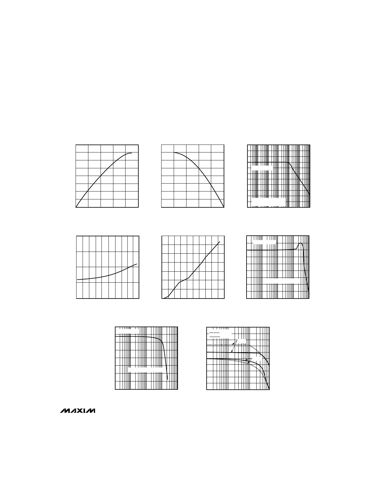
OUTPUT SINK CAPABILITY vs.
OUTPUT PULL-DOWN VOLTAGE
2
10
MAX503-1
OUTPUT PULL-DOWN VOLTAGE (V)
OUTPUT SINK CAPABILITY (mA)
0.6
6
4
0.2
0.4
8
1.0
14
16
6
0
0
4
OUTPUT SOURCE CAPABILITY vs.
OUTPUT PULL-UP VOLTAGE
1
5
MAX503-2
OUTPUT PULL-UP VOLTAGE (V)
OUTPUT SOURCE CAPABILITY (mA)
3
3
2
1
2
4
5
7
8
300
230
-60
-20
60
140
SUPPLY CURRENT vs. TEMPERATURE
250
280
TEMPERATURE (°C)
SUPPLY CURRENT (
µ
A)
20
100
260
290
270
240
-40
0
40
80
120
MAX503-5
4
-14
1
100
100k
GAIN vs. FREQUENCY
-12
MAX503-6
FREQUENCY (Hz)
GAIN (dB)
-8
-4
0
2
-2
-6
-10
1k
10k
REFIN = 4Vp-p
DUAL SUPPLIES (±5V)
__________________________________________Typical Operating Characteristics
(Single +5V supply, unity gain, code = all 1s, T
A
= +25°C, unless otherwise noted.)
-110
0
1
10
1k
100k
ANALOG FEEDTHROUGH vs.
FREQUENCY
-30
-70
MAX503-3
FREQUENCY (Hz)
ANALOG FEEDTHROUGH (dB)
100
10k
1M
-100
-90
-80
-60
-50
-40
-20
-10
REFIN = 2Vp-p
CODE = ALL 0s,
DUAL SUPPLIES (±5V)
2.055
2.045
-60
120
REFERENCE VOLTAGE vs.
TEMPERATURE
MAX503-4
TEMPERATURE (
°
C)
REFERENCE VOLTAGE (V)
60
2.050
-20
20
80 100
40
0
-40
140
80
0
10
1k
100k
AMPLIFIER SIGNAL-TO- NOISE RATIO
10
MAX503-7
FREQUENCY (Hz)
SIGNAL-TO-NOISE RATIO (dB)
20
40
60
30
50
70
10k
100
REFIN = 4Vp-p
DUAL SUPPLIES (±5V)
200
-300
1
GAIN AND PHASE vs.
FREQUENCY
-100
100
FREQUENCY (kHz)
GAIN (dB)
10
100
0
-200
800
-180
0
180
GAIN
PHASE
(G = 2)
(G = 1)
PHASE SHIFT (Degrees)
MAX503-8
MAX503
5V, Low-Power, Parallel-Input,
Voltage-Output, 10-Bit DAC
6
_______________________________________________________________________________________
____________________________Typical Operating Characteristics (continued)
(Single +5V supply, unity gain, code = all 1s, T
A
= +25°C, unless otherwise noted.)
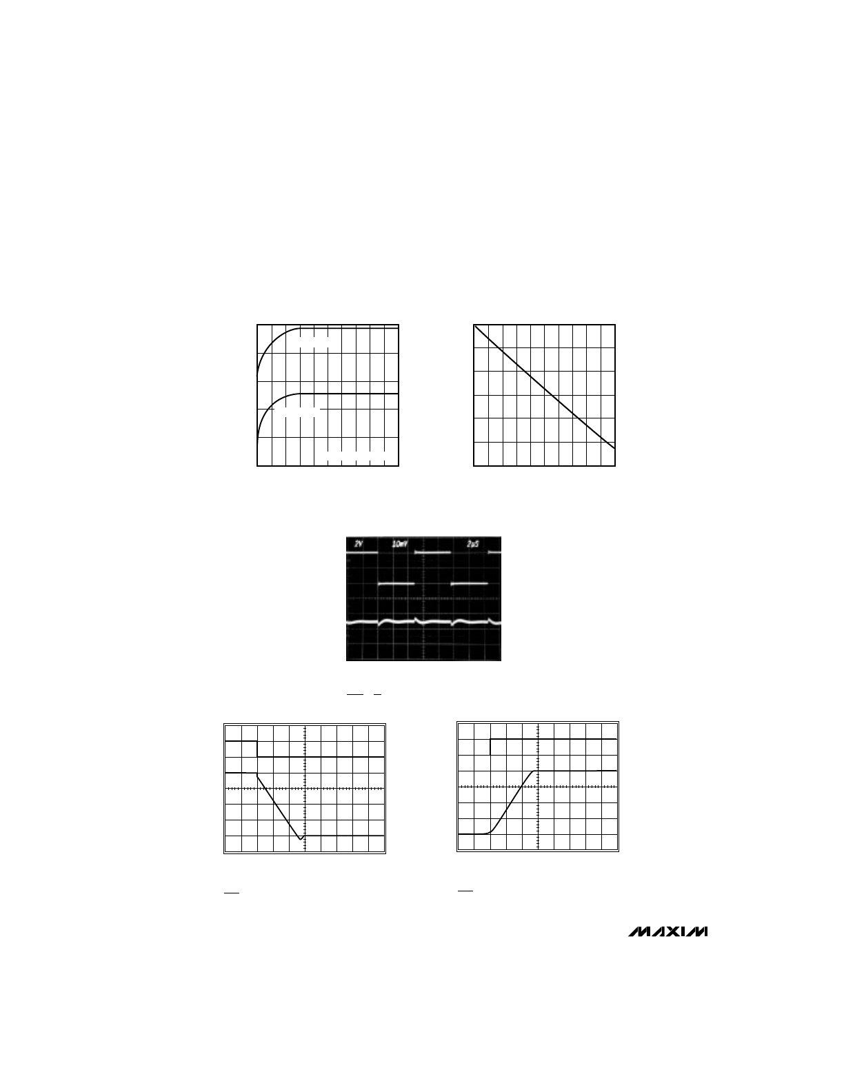
DIGITAL FEEDTHROUGH
A
B
A: S0, S1, D0–D9 = 100kHz, 4Vp-p
B: VOUT, 10mV/div
LDAC = CS = HIGH
2
µ
s/div
A: DIGITAL INPUTS RISING EDGE,
B: VOUT
,
NO LOAD, 1V/div
DUAL SUPPLY (±5V)
LDAC = LOW
BIPOLAR CONFIGURATION
V
REFIN
= 2V
A
B
SETTLING TIME (RISING)
5
µ
s/div
2.0480
2.0450
0
5.0
REFERENCE OUTPUT VOLTAGE
vs. REFERENCE LOAD CURRENT
2.0455
2.0475
MAX503-10
REFERENCE LOAD CURRENT (mA)
REFERENCE OUTPUT (V)
3.0
2.0465
2.0460
1.0
2.0
4.0
2.0470
0.5
1.5
2.5
3.5
4.5
A: DIGITAL INPUTS FALLING EDGE, 5V/div
B: VOUT, NO LOAD, 1V/div
DUAL SUPPLY (±5V)
LDAC = LOW
BIPOLAR CONFIGURATION
V
REFIN
= 2V
A
SETTLING TIME (FALLING)
B
5µs/div
0
0
500
SUPPLY CURRENT vs. REFIN
50
250
REFIN (mV)
SUPPLY CURRENT (
µ
A)
300
150
100
100
200
400
200
50
150
250
350
450
EXTERNAL REFERENCE
REFGND = AGND
REFGND = V
DD
MAX503-9
MAX503
5V, Low-Power, Parallel-Input,
Voltage-Output, 10-Bit DAC
_______________________________________________________________________________________
7
PIN
FUNCTION
1
D7 input when A0 = A1 = 1, or S1 input when A0 = 0 and A1 = 1. Always set S1 to 0.*
2
D8 input when A0 = A1 = 1, or D0 input when A0 = 0 and A1 = 1.*
3
D9 input when A0 = A1 = 1, or D1 input when A0 = 0 and A1 = 1.*
4
D2 Input Data, or tie to S0 and multiplex when A0 = 1 and A1 = 0.*
______________________________________________________________Pin Description
NAME
D7/ S1
D8/ D0
D9/ D1
D2
5
D3
D3 Input Data, or tie to S1 and multiplex when A0 = 1 and A1 = 0.*
6
D4
D4 Input Data, or tie to D0 and multiplex when A0 = 1 and A1 = 0.*
7
D5
D5 Input Data, or tie to D1 and multiplex when A0 = 1 and A1 = 0.*
8
A0
Address Line A0. With A1, used to multiplex 4 of 12 data lines to load low (NBL), middle (NBM),
and high (NBH) 4-bit nibbles. (12 bits can also be loaded as 8+4.)
9
A1
Address Line A1. Set A0 = A1 = 0 for NBL and NBM, A0 = 0 and A1 = 1 for NBL, A0 = 1 and A1 =
0 for NBM, or A0 = A1 = 1 for NBH. See Table 2 for complete input latch addressing.
10
WR
Write Input (active low). Used with CS to load data into the input latch selected by A0 and A1.
11
CS
Chip Select (active low). Enables addressing and writing to this chip from common bus lines.
12
DGND
Digital Ground
13
REFIN
Reference Input. Input for the R-2R DAC. Connect an external reference to this pin or a jumper to
REFOUT (pin 18) to use the internal 2.048V reference.
14
AGND
Analog Ground
15
CLR
Clear (active low). A low on CLR resets the DAC latches to all 0s.
16
LDAC
Load DAC Input (active low). Driving this asynchronous input low transfers the contents of the input
latch to the DAC latch and updates VOUT.
17
REFGND
Reference Ground must be connected to AGND when using the internal reference. Connect to V
DD
to disable the internal reference and save power.
18
REFOUT
Reference Output. Output of the internal 2.048V reference. Tie to REFIN to drive the R-2R DAC.
19
V
SS
Negative Power Supply. Usually ground for single-supply or -5V for dual-supply operation.
20
VOUT
Voltage Output. Op-amp buffered DAC output.
21
RFB
Feedback Pin. Op-amp feedback resistor. Always connect to VOUT.
22
ROFS
Offset Resistor Pin. Connect to VOUT for G = 1, to AGND for G = 2, or to REFIN for bipolar output.
23
V
DD
Positive Power Supply (+5V)
24
D6/S0
D6 input when A0 = A1 = 1, or S0 input when A0 = 0 and A1 = 1. Always set S0 to 0.*
* This applies to 4 + 4 + 4 input loading mode. See Table 2 for 8 + 4 input loading mode.
MAX503
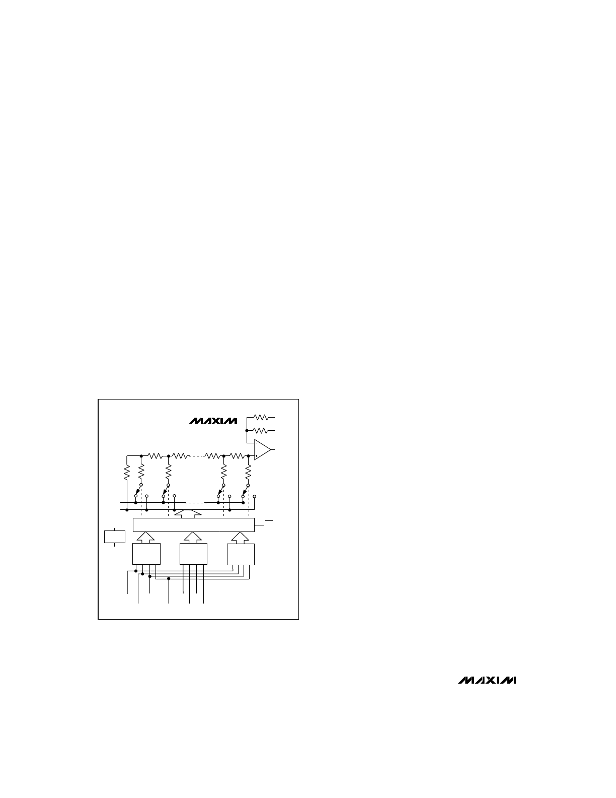
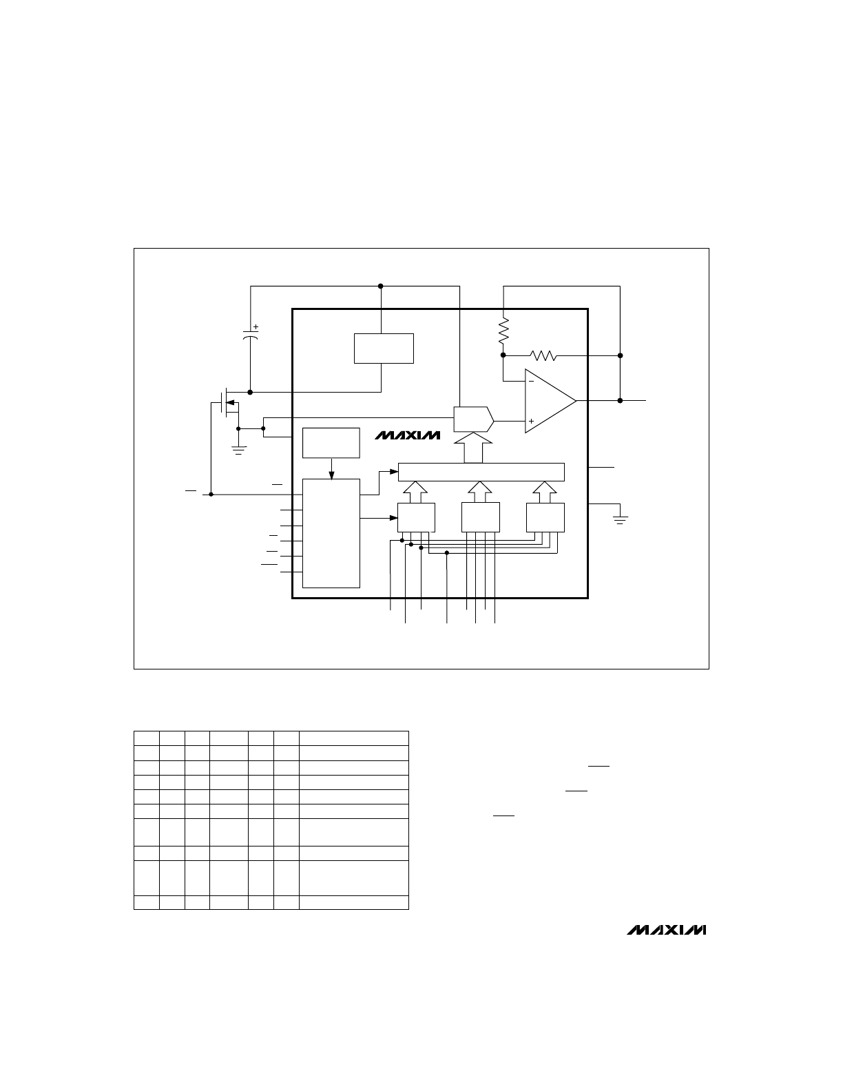
________________Detailed Description
The MAX503 consists of a parallel-input logic interface, a
10-bit R-2R ladder, a reference, and an op amp. The
Functional Diagram shows the control lines and signal
flow through the input data latch to the DAC latch, as well
as the 2.048V reference and output op amp. Total supply
current is typically 250µA with a single +5V supply. This
circuit is ideal for battery-powered, microprocessor-con-
trolled applications where high accuracy, no adjustments,
and minimum component count are key requirements.
R-2R Ladder
The MAX503 uses an “inverted” R-2R ladder network with
a BiCMOS op amp to convert 10-bit digital data to analog
voltage levels. Figure 1 shows a simplified diagram of the
R-2R DAC and op amp. Unlike a standard DAC, the
MAX503 uses an “inverted” ladder network. Normally, the
REFIN pin is the current output of a standard DAC and
would be connected to the summing junction, or virtual
ground, of an op amp. In this standard DAC configura-
tion, however, the output voltage would be the inverse of
5V, Low-Power, Parallel-Input,
Voltage-Output, 10-Bit DAC
8
_______________________________________________________________________________________
2R
2R
2R
2R
2R
R
R
R
MSB
OUTPUT
BUFFER
VOUT
RFB
ROFS
MAX503
2R
2R
REFIN
AGND
DAC LATCH
R
=
80k
Ω
LSB
NBL
INPUT
LATCH
NBH
INPUT
LATCH
NBM
INPUT
LATCH
D6/S0
D7/S1
D8/D0
D2
D9/D1
D4
D3
D5
2.048V
REFOUT
REFGND
*
SHOWN FOR ALL 1s
*
LSB
MSB
CLR
Figure 1. Simplified MAX503 DAC Circuit
the reference voltage. The MAX503’s topology makes the
ladder output voltage the same polarity as the reference
input, making the device suitable for single-supply oper-
ation. The BiCMOS op amp is then used to buffer, invert,
or amplify the ladder signal.
Ladder resistors are nominally 80k
Ω
to conserve power
and are laser trimmed for gain and linearity. The input
impedance at REFIN is code dependent. When the DAC
register is all 0s, all rungs of the ladder are grounded
and REFIN is open or no load. Maximum loading (mini-
mum REFIN impedance) occurs at code 010101....
Minimum reference input impedance at this code is guar-
anteed to be not less than 40k
Ω
.
The REFIN and REFOUT pins allow the user to choose
between driving the R-2R ladder with the on-chip refer-
ence or an external reference. REFIN may be below ana-
log ground when using dual supplies. See the
External
Reference and Four-Quadrant Multiplication sections for
more information.
Internal Reference
The on-chip reference is laser trimmed to generate
2.048V at REFOUT. The output stage can source and
sink current so REFOUT can settle to the correct volt-
age quickly in response to code-dependent loading
changes. Typically, source current is 5mA and sink
current is 100µA.
REFOUT connects the internal reference to the R-2R
DAC ladder at REFIN. The R-2R ladder draws 50µA
maximum load current. If any other connection is made
to REFOUT, ensure that the total load current is less
than 100µA to avoid gain errors.
A separate REFGND pin is provided to isolate refer-
ence currents from other analog and digital ground
currents. To achieve specified noise performance, con-
nect a 33µF capacitor from REFOUT to REFGND (see
Figure 2). Using smaller capacitance values increases
noise, and values less than 3.3µF may compromise the
reference’s stability. For applications requiring the low-
est noise, insert a buffered RC filter between REFOUT
and REFIN. When using the internal reference,
REFGND must be connected to AGND. In applications
not requiring the internal reference, connect REFGND
to V
DD
, which shuts down the reference. This saves
typically 100µA of V
DD
supply current and eliminates
the need for C
REFOUT
.
Output Buffer
The output amplifier uses a folded cascode input stage
and a type AB output stage. Large output devices with
low series resistance allow the output to swing to
ground in single-supply operation. The output buffer is
unity-gain stable. Input offset voltage and supply cur-
rent are laser trimmed. Settling time is 25µs to 0.01% of
final value. The output is short-circuit protected and
can drive a 2k
Ω
load with more than 100pF of load
capacitance. The op amp may be placed in unity-gain
(G = 1), in a gain of two (G = 2), or in a bipolar-output
mode by using the ROFS and RFB pins. These pins are
used to define a DAC output voltage range of 0V to
+2.048V, 0V to +4.096V or ±2.048V, by connecting
ROFS to VOUT, GND, or REFIN. RFB is always con-
nected to VOUT. Table 1 summarizes ROFS usage.
External Reference
An external reference in the range (V
SS
+ 2V) to
(V
DD
- 2V) may be used with the MAX503 in dual-sup-
ply, unity-gain operation. In single-supply, unity-gain
operation, the reference must be positive and may not
exceed (V
DD
- 2V). The reference voltage determines
the DAC’s full-scale output.
If an upgrade to the internal reference is required, the
2.5V MAX873A is ideal: ±15mV initial accuracy,
7ppm/°C (max) temperature coefficient.
Power-On Reset
An internal power-on reset (POR) circuit forces the
DAC register to reset to all 0s when V
DD
is first applied.
The POR pulse is typically 1.3µs; however, it may take
2ms for the internal reference to charge its large filter
capacitor and settle to its trimmed value.
In addition to POR, a clear (CLR) pin, when held low,
sets the DAC register to all 0s. CLR operates asynchro-
nously and independently from chip select (CS). With
the DAC input at all 0s, the op-amp output is at zero for
unity-gain and G = 2 configurations, but it is at -V
REF
for the bipolar configuration.
Shutdown Mode
The MAX503 is designed for low power consumption.
Understanding the circuit allows power consumption
management for maximum efficiency. In single-supply
mode (V
DD
= +5V, V
SS
= GND) the initial supply cur-
rent is typically only 160µA, including the reference, op
amp, and DAC. This low current occurs when the
power-on reset circuit clears the DAC to all 0s and
forces the op-amp output to zero (unipolar mode only).
See the Supply Current vs. REFIN graph in the
Typical
Operating Characteristics. Under this condition, there
is no internal load on the reference (DAC = all 0s,
REFIN is open circuit) and the op amp operates at its
minimum quiescent current. The CLR signal resets the
MAX503 to these same conditions and can be used to
control a power-saving mode when the DAC is not
being used by the system.
MAX503
5V, Low-Power, Parallel-Input,
Voltage-Output, 10-Bit DAC
_______________________________________________________________________________________
9
ROFS
CONNECTED TO:
DAC OUTPUT
RANGE
OP-AMP
GAIN
VOUT
0V to 2.048V
G = 1
AGND
0V to 4.096V
G = 2
REFIN
-2.048V to +2.048V
Bipolar
Note:
Assumes RFB = VOUT and REFIN = REFOUT = 2.048V
Table 1. ROFS Usage
Figure 2. Reference Noise vs. Frequency
300
50
1
10
100
100
MAX503-FIG02
FREQUENCY (kHz)
REFERENCE NOISE (µV
RMS
)
150
200
250
0
0.1
1000
TOTAL
REFERENCE
NOISE
R
S
REFOUT
C
REFOUT
C
S
TEK 7A22
C
REFOUT
= 3.3
µ
F
C
REFOUT
= 47
µ
F
SINGLE POLE ROLLOFF
1.8
1.6
1.4
1.2
1.0
0.8
0.6
0.4
0.2
0.0
REFERENCE NOISE (mVp-p)
An additional 110µA of supply current can be saved
when the internal reference is not used by connecting
REFGND to V
DD
. A low on-resistance N-channel FET,
such as the 2N7002, can be used to turn off the internal
reference to create a shutdown mode with minimum
current drain (Figure 3). When CLR is high, the transis-
tor pulls REFGND to AGND and the reference and DAC
operate normally. When CLR goes low, REFGND is
pulled up to V
DD
and the reference is shut down. At the
same time, CLR resets the DAC register to all 0s, and
the op-amp output goes to 0V for unity-gain and
G = 2 modes. This reduces the total single-supply
operating current from 250µA (400µA max) to typically
40µA in shutdown mode.
MAX503
5V, Low-Power, Parallel-Input,
Voltage-Output, 10-Bit DAC
10
______________________________________________________________________________________
MAX503
MAX503
10-BIT DAC LATCH
NBL
INPUT
LATCH
NBH
INPUT
LATCH
NBM
INPUT
LATCH
D6/S0
D7/S1
D8/D0
D2
D9/D1
D4
D3
D5
POWER-ON
RESET
CONTROL
LOGIC
DAC
A0
A1
CS
WR
LDAC
CLR
33
µ
F
2.048V
REFERENCE
REFOUT
REFIN
ROFS
RFB
V
OUT
+5V
V
SS
DGND
2N7002
REFGND
AGND
V
DD
CLR
Figure 3. Low-Current Shutdown Mode
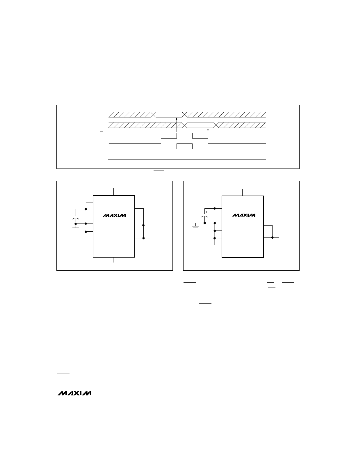
CLR CS WR LDAC
A0
A1
DATA UPDATED
L
X
X
X
X
X
Reset DAC latches
H
H
X
H
X
X
No operation
H
X
H
H
X
X
No operation
H
L
L
H
H
H
NBH (D6–D9)
H
L
L
H
H
L
NBM (D2–D5)
H
L
L
H
L
H
NBL (S0 = 0, S1 = 0,
D0, D1)
H
H
H
L
X
X
Update DAC only
H
L
L
X
L
L
NBL and NBM (S0, S1,
D0–D5), DAC not
updated
H
L
L
L
H
H
NBH and update DAC
Table 2. Input Latch Addressing
MAX503
5V, Low-Power, Parallel-Input,
Voltage-Output, 10-Bit DAC
______________________________________________________________________________________
11
V
IH
V
IL
DATA BITS
(8-BIT BYTE
OR 4-BIT NIBBLE)
A0–A1
V
IL
V
IH
ADDRESS BUS VALID
t
AWH
t
CWS
t
WR
t
CWH
t
AWS
t
DS
t
DH
DATA BUS
VALID
NOTE: TIMING MEASUREMENT REFERENCE LEVEL IS
V
IH +
V
IL
2
t
CLR
CS
WR
CLR
LDAC
t
LDAC
Figure 4. MAX503 Write-Cycle Timing Diagram
A small error voltage is added to the reference output
by the reference current flowing through the N-channel
pull-down transistor. The switch’s on resistance should
be less than 5
Ω
. A typical reference current of 100µA
would add 0.5mV to REFOUT. Since the reference cur-
rent and on resistance increase with temperature, the
overall temperature coefficient will degrade slightly.
As data is loaded into the DAC and the output moves
above GND, the op-amp quiescent current increases to
its nominal value and the total operating current aver-
ages 250µA. Using dual supplies (±5V), the op amp is
fully biased continuously, and the V
DD
supply current is
more constant at 250µA. The V
SS
current is typically
150µA.
The MAX503 logic inputs are compatible with TTL and
CMOS logic levels. However, to achieve the lowest
power dissipation, drive the digital inputs with rail-to-rail
CMOS logic. With TTL logic levels, the power require-
ment increases by a factor of approximately 2.
Parallel Logic Interface
In order to provide hardware and software compatibility
with the 12-bit MAX530, the MAX503 employs a 12-bit
digital interface. As shown in Figure 3, there is actually
a 12-bit input latch, and therefore 12 bits of data should
be written. The two least significant bits (S1 and S0) are
sub-LSB, and must always be 0s. Designed to interface
with 4-bit, 8-bit, and 16-bit microprocessors (µPs), the
MAX503 uses 8 data pins and double-buffered logic
inputs to load data as 4 + 4 + 4 or 8 + 4. The 12-bit
DAC latch is updated simultaneously through the con-
trol signal LDAC. Signals A0, A1, WR, and CS select
which input latches to update. The 12-bit data is bro-
ken down into nibbles (NB); NBL is the enable signal
for the lowest 4 bits (S0, S1, D0, D1), NBM is the
enable for the middle 4 bits, and NBH is the enable for
the highest and most significant 4 bits. Table 2 lists the
address decoding scheme.
Refer to Figure 4 for the MAX503 write-cycle timing
diagram.
MAX503
5V, Low-Power, Parallel-Input,
Voltage-Output, 10-Bit DAC
12
______________________________________________________________________________________
A0 = 1, A1 = 1
NBH
NBM
NBL
CS
WR
LDAC
A0 = 1, A1 = 0
A0 = 0, A1 = 1
DAC UPDATE
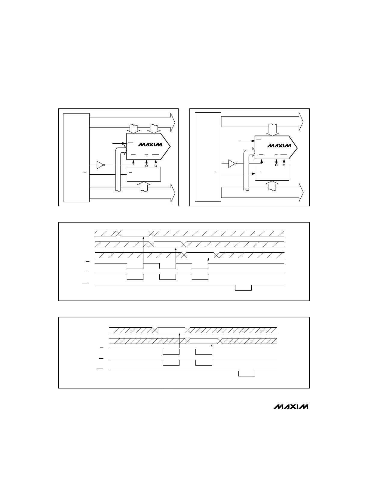
Figure 6. 4-Bit µP Timing Sequence
A0 = A1 = 1
A0 = A1 = 0
DAC UPDATE
NBH
NBL & NBM
CS
WR
LDAC
Figure 8a. 8-Bit and 16-Bit µP Timing Sequence Using LDAC
Figure 5. 4-Bit µP Interface
DATA BUS
D0–D3
D0–D3
S0, S1, D0, D1
D2–D5
MC6800
FROM
SYSTEM
RESET
∅
2
R/W
CLR
WR
CS
LDAC
EN
DECODER
A0–A15
A13–A15
ADDRESS BUS
A0, A1
A0, A1
D0–D3
MAX503
Figure 7. 8-Bit and 16-Bit µP Interface
D0–D7
DATA BUS
D0–D7
S0, S1, D0–D5
MC6809
FROM
SYSTEM
RESET
CLR
A0–A1
WR
CS LDAC
E
R/W
A0–A15
A13–A15
A0
ADDRESS BUS
EN
DECODER
MAX503
MAX503
5V, Low-Power, Parallel-Input,
Voltage-Output, 10-Bit DAC
______________________________________________________________________________________
13
A0 = A1 = 0
A0 = A1 = 1
DAC UPDATE
NBH
NBL & NBM
CS
WR
LDAC = 0 (DAC LATCH IS TRANSPARENT)
Figure 8b. 8-Bit and 16-Bit µP Timing Sequence with LDAC = 0
Figure 5 shows the circuit configuration for a 4-bit µP
application. Figure 6 shows the corresponding timing
sequence. The 4 low bits (S0, S1, D0, D1) are connect-
ed in parallel to the other 4 bits (D2–D5) and then to the
µP bus. Address lines A0 and A1 enable the input data
latches for the high, middle, or low data nibbles. The µP
sends chip select (CS) and write (WR) signals to latch
in each of three nibbles in three cycles when the data is
valid.
Figure 7 shows a typical interface to an 8-bit or a 16-bit
µP. Connect 8 data bits from the data bus to pins S0,
S1, and D0–D5 on the MAX503. With LDAC held high,
the user can load NBH or NBL + NBM in any order.
Figure 8a shows the corresponding timing sequence.
For fastest throughput, use Figure 8b’s sequence.
Address lines A0 and A1 are tied together and the DAC
is loaded in 2 cycles as 8 + 4. In this scheme, with
LDAC held low, the DAC latch is transparent. Always
load NBL and NBM first, followed by NBH.
LDAC is asynchronous with respect to WR. If LDAC is
brought low before or at the same time WR goes high,
LDAC must remain low for at least 50ns to ensure the
correct data is latched. Data is latched into DAC regis-
ters on LDAC’s rising edge.
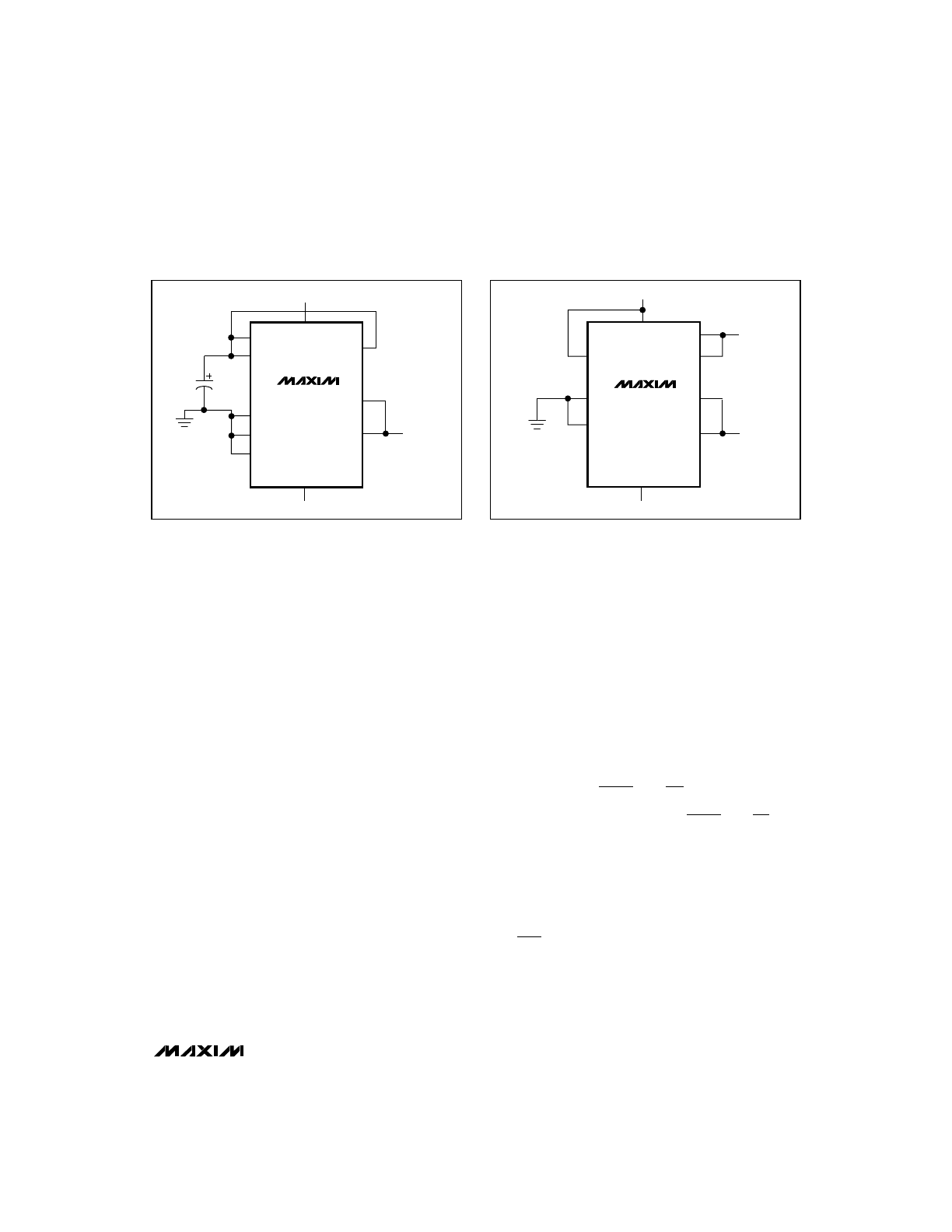
Unipolar Configuration
The MAX503 is configured for a 0V to V
REFIN
unipolar
output range by connecting ROFS and RFB to VOUT
(Figure 9). The converter operates from either single or
dual supplies in this configuration. See Table 3 for the
DAC-latch contents (input) vs. the analog VOUT (output).
In this range, 1LSB = V
REFIN
(2
-10
).
A 0V to 2V
REFIN
unipolar output range is set up by con-
necting ROFS to AGND and RFB to VOUT (Figure 10).
Table 4 shows the DAC-latch contents vs. VOUT. The
MAX503 operates from either single or dual supplies in
this mode. In this range, 1LSB = (2)(V
REFIN
)(2
-10
) =
(V
REFIN
)(2
-9
).
33µF
REFIN
REFOUT
AGND
DGND
REFGND
V
DD
V
SS
ROFS
RFB
VOUT
V
OUT
0V TO -5V
+5V
G = 1
MAX503
33µF
REFIN
REFOUT
AGND
DGND
REFGND
V
DD
V
SS
ROFS
RFB
VOUT
V
OUT
0V TO -5V
+5V
G = 2
MAX503
Figure 9. Unipolar Configuration (0V to +2.048V Output)
Figure 10. Unipolar Configuration (0V to +4.096V Output)
MAX503
5V, Low-Power, Parallel-Input,
Voltage-Output, 10-Bit DAC
14
______________________________________________________________________________________
INPUT*
OUTPUT
1111
1111
11(00)
1000
0000
01(00)
1000
0000
00(00)
0111
1111
11(00)
0000
0000
01(00)
0000
0000
00(00)
(V
REFIN
)
1023
1024
(V
REFIN
)
513
1024
(V
REFIN
)
512
1024
(V
REFIN
)
511
1024
(V
REFIN
)
1
1024
OV
= +V
REFIN
/2
Table 3. Unipolar Binary Code Table
(0V to V
REFIN
Output), Gain = 1
INPUT*
OUTPUT
1111
1111
11(00)
1000
0000
01(00)
1000
0000
00(00)
0111
1111
11(00)
0000
0000
01(00)
0000
0000
00(00)
+2 (V
REFIN
)
1023
1024
+2 (V
REFIN
)
513
1024
+2 (V
REFIN
)
512
1024
+2 (V
REFIN
)
511
1024
+2 (V
REFIN
)
1
1024
OV
= +V
REFIN
Table 4. Unipolar Binary Code Table
(0V to 2V
REFIN
Output), Gain = 2
INPUT*
OUTPUT
1111
1111
11(00)
1000
0000
01(00)
1000
0000
00(00)
0111
1111
11(00)
0000
0000
01(00)
0000
0000
00(00)
(+V
REFIN
)
511
512
(+V
REFIN
)
1
512
(-V
REFIN
)
1
512
(-V
REFIN
)
511
512
0V
(-V
REFIN
)
512
512
= -V
REFIN
Table 5. Bipolar (Offset Binary) Code
Table (-V
REFIN
to +V
REFIN
Output)
Bipolar Configuration
A -V
REFIN
to +V
REFIN
bipolar range is set up by con-
necting ROFS to REFIN and RFB to VOUT, and operat-
ing from dual (±5V) supplies (Figure 11). Table 5
shows the DAC-latch contents (input) vs. VOUT (out-
put). In this range, 1LSB = V
REFIN
(2
-9
).
Four-Quadrant Multiplication
The MAX503 can be used as a four-quadrant multiplier
by connecting ROFS to REFIN and RFB to VOUT, and
using (1) an offset binary digital code, (2) bipolar
power supplies, and (3) a bipolar analog input at
REFIN within the range V
SS
+ 2V to V
DD
- 2V, as shown
in Figure 12.
In general, a 10-bit DAC’s output is D(V
REFIN
)(G),
where “G” is the gain (1 or 2) and “D” is the binary rep-
resentation of the digital input divided by 2
10
or 1,024.
This formula is precise for unipolar operation. However,
for bipolar, offset binary operation, the MSB is really a
polarity bit. No resolution is lost because the number of
steps is the same. The output voltage, however, has
been shifted from a range of, for example, 0V to
4.096V (G = 2) to a range of -2.048V to +2.048V.
Keep in mind that when using the DAC as a four-quad-
rant multiplier, the scale is skewed. The negative full
scale is -V
REFIN
, while the positive full scale is
+V
REFIN
- 1LSB.
* Write 10-bit data words with two sub-LSB 0s because the
DAC input latch is 12 bits wide.
* Write 10-bit data words with two sub-LSB 0s because the
DAC input latch is 12 bits wide.
* Write 10-bit data words with two sub-LSB 0s because the
DAC input latch is 12 bits wide.
MAX503
5V, Low-Power, Parallel-Input,
Voltage-Output, 10-Bit DAC
______________________________________________________________________________________
15
33µF
REFIN
REFOUT
AGND
DGND
REFGND
ROFS
RFB
VOUT
V
OUT
-5V
+5V
MAX503
Figure 11. Bipolar Configuration (-2.048V to +2.048V Output)
Figure 12. Four-Quadrant Multiplying Circuit
REFGND
AGND
DGND
REFIN
V
DD
V
SS
ROFS
RFB
VOUT
V
OUT
-5V
+5V
REFIN
MAX503
__________Applications Information
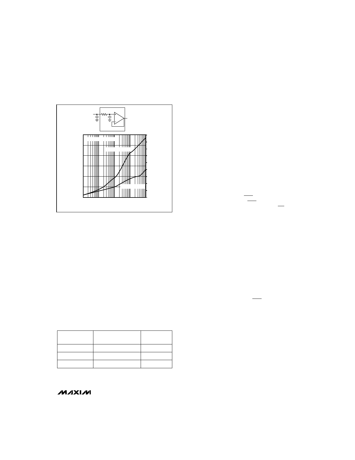
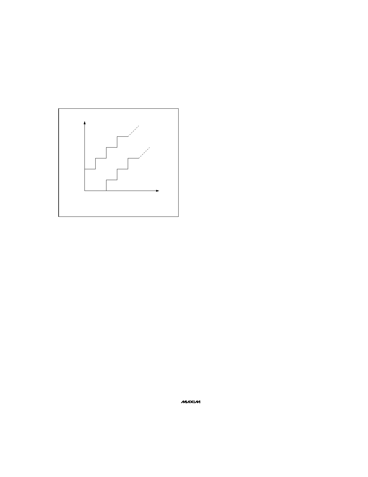
Single-Supply Linearity
As with any amplifier, the MAX503’s output op amp off-
set can be positive or negative. When the offset is posi-
tive, it is easily accounted for. However, when the offset
is negative, the output cannot follow linearly when there
is no negative supply. In that case, the amplifier output
(VOUT) remains at ground until the DAC voltage is suffi-
cient to overcome the offset and the output becomes
positive. The resulting transfer function is shown in
Figure 13.
Normally, linearity is measured after allowing for zero
error and gain error. Since, in single-supply operation,
the actual value of a negative offset is unknown, it can-
not be accounted for during test. In the MAX503, linear-
ity and gain error are measured from code 3 to code
1023 (see Note 2 under
Electrical Characteristics). The
output amplifier offset does not affect monotonicity, and
these DACs are guaranteed monotonic starting with
code zero. In dual-supply operation, linearity and gain
error are measured from code 0 to 1023.
Power-Supply Bypassing
and Ground Management
Best system performance is obtained with printed cir-
cuit boards that use separate analog and digital ground
planes. Wire-wrap boards are not recommended. The
two ground planes should be connected together at the
low-impedance power-supply source.
AGND and REFGND should be connected together,
and then to DGND at the chip. For single-supply appli-
cations, connect V
SS
to AGND at the chip. The best
ground connection may be achieved by connecting
the AGND, REFGND, and DGND pins together and
connecting that point to the system analog ground
plane. If DGND is connected to the system digital
ground, digital noise may get through to the DAC’s ana-
log portion.
Bypass V
DD
(and V
SS
in dual-supply mode) with a
0.1µF ceramic capacitor connected between V
DD
and
AGND (and between V
SS
and AGND). Mount the
capacitors with short leads close to the device.
AC Considerations
Digital Feedthrough
High-speed data at any of the digital input pins may
couple through the DAC package and cause internal
stray capacitance to appear as noise at the DAC out-
put, even though LDAC and CS are held high (see
Typical Operating Characteristics). This digital
feedthrough is tested by holding LDAC and CS high
and toggling the data inputs from all 1s to all 0s.
Analog Feedthrough
Because of internal stray capacitance, higher-frequen-
cy analog input signals at REFIN may couple to the
output, even when the input digital code is all 0s, as
shown in the
Typical Operating Characteristics graph
Analog Feedthrough vs. Frequency. It is tested by set-
ting CLR to low (which sets the DAC latches to all 0s)
and sweeping REFIN.
MAX503
5V, Low-Power, Parallel-Input,
Voltage-Output, 10-Bit DAC
1
2
3
4
5
1
2
3
4
5
0
POSITIVE OFFSET
NEGATIVE OFFSET
DAC CODE (LSBs)
OUTPUT (LSBs)
Figure 13. Single-Supply DAC Transfer Function
Maxim cannot assume responsibility for use of any circuitry other than circuitry entirely embodied in a Maxim product. No circuit patent licenses are
implied. Maxim reserves the right to change the circuitry and specifications without notice at any time.
16
__________________Maxim Integrated Products, 120 San Gabriel Drive, Sunnyvale, CA 94086 (408) 737-7600
© 1994 Maxim Integrated Products
Printed USA
is a registered trademark of Maxim Integrated Products.