
For free samples & the latest literature: http://www.maxim-ic.com, or phone 1-800-998-8800
_______________General Description
The MAX500 is a quad, 8-bit, voltage-output digital-to-
analog converter (DAC) with a cascadable serial inter-
face. The IC includes four output buffer amplifiers and
input logic for an easy-to-use, two- or three-wire serial
interface. In a system with several MAX500s, only one
serial data line is required to load all the DACs by cas-
cading them. The MAX500 contains double-buffered
logic and a 10-bit shift register that allows all four DACs
to be updated simultaneously using one control signal.
There are three reference inputs so the range of two of
the DACs can be independently set while the other two
DACs track each other.
The MAX500 achieves 8-bit performance over the full
operating temperature range without external trimming.
________________________Applications
Minimum Component Count Analog Systems
Digital Offset/Gain Adjustment
Industrial Process Control
Arbitrary Function Generators
Automatic Test Equipment
____________________________Features
♦
Buffered Voltage Outputs
♦
Double-Buffered Digital Inputs
♦
Microprocessor and TTL/CMOS Compatible
♦
Requires No External Adjustments
♦
Two- or Three-Wire Cascadable Serial Interface
♦
16-Pin DIP/SO Package and 20-Pin LCC
♦
Operates from Single or Dual Supplies
______________Ordering Information
MAX500
CMOS, Quad, Serial-Interface
8-Bit DAC
________________________________________________________________
Maxim Integrated Products
1
TOP VIEW
16
15
14
13
12
11
10
9
1
2
3
4
5
6
7
8
V
OUT
C
V
OUT
D
V
DD
V
REF
C
V
REF
A/B
V
SS
V
OUT
A
V
OUT
B
MAX500
V
REF
D
SRO
SCL
LOAD
SDA
LDAC
DGND
AGND
DIP/SO
_________________Pin Configurations
MAX500
V
OUT
A
DAC A
DAC B
DAC C
DAC D
V
REF
C
V
REF
A/B
DAC
REG A
INPUT
REG A
DAC
REG B
INPUT
REG B
DAC
REG C
INPUT
REG C
DAC
REG D
INPUT
REG D
10/11-
BIT
SHIFT
REGISTER
CONTROL
LOGIC
LOAD
SCL
SDA
V
OUT
B
V
OUT
C
V
OUT
D
SRO
V
DD
DGND V
SS
AGND
V
REF
D
DATA BUS
LDAC
________________Functional Diagram
19-1016; Rev 2; 2/96
PART
MAX500ACPE
MAX500BCPE
MAX500ACWE
0°C to +70°C
0°C to +70°C
0°C to +70°C
TEMP. RANGE PIN-PACKAGE
16 Plastic DIP
16 Plastic DIP
16 Wide SO
MAX500BCWE
0°C to +70°C
16 Wide SO
MAX500BC/D
0°C to +70°C
Dice*
MAX500AEPE -40°C to +85°C
16 Plastic DIP
MAX500BEPE -40°C to +85°C
16 Plastic DIP
MAX500AEWE -40°C to +85°C
16 Wide SO
MAX500BEWE -40°C to +85°C
16 Wide SO
MAX500AEJE -40°C to +85°C
16 CERDIP
MAX500BEJE -40°C to +85°C
16 CERDIP
MAX500AMJE -55°C to +125°C
16 CERDIP
MAX500BMJE -55°C to +125°C
16 CERDIP
ERROR (LSB)
±1
±2
±1
±2
±2
±1
±2
±1
±2
±1
±2
±1
±2
*Contact factory for dice specifications.
Pin Configurations continued on last page.
MAX500AMLP -55°C to +125°C
20 LCC
±1
MAX500BMLP -55°C to +125°C
20 LCC
±2
MAX500
CMOS, Quad, Serial-Interface
8-Bit DAC
2
_______________________________________________________________________________________
ABSOLUTE MAXIMUM RATINGS
ELECTRICAL CHARACTERISTICS—Dual Supplies
(V
DD
= +11.4V to +16.5V, V
SS
= -5V ±10%, AGND = DGND = 0V, V
REF
= +2V to (V
DD
- 4V), T
A
= T
MIN
to T
MAX
, unless otherwise noted.)
Stresses beyond those listed under “Absolute Maximum Ratings” may cause permanent damage to the device. These are stress ratings only, and functional
operation of the device at these or any other conditions beyond those indicated in the operational sections of the specifications is not implied. Exposure to
absolute maximum rating conditions for extended periods may affect device reliability.
Power Requirements
V
DD
to AGND...........................................................-0.3V, +17V
V
DD
to DGND ..........................................................-0.3V, +17V
V
SS
to DGND ..................................................-7V, (V
DD
+ 0.3V)
V
DD
to V
SS
...............................................................-0.3V, +24V
Digital Input Voltage to DGND ....................-0.3V, (V
DD
+ 0.3V)
V
REF
to AGND .............................................-0.3V, (V
DD
+ 0.3V)
V
OUT
to AGND (Note 1)...............................-0.3V, (V
DD
+ 0.3V)
Power Dissipation (T
A
= +70°C)
Plastic DIP (derate 10.53mW/°C above +70°C) ............842mW
Wide SO (derate 9.52mW/°C above +70°C)................762mW
CERDIP (derate 10.00mW/°C above +70°C) ...............800mW
LCC (derate 9.09mW/°C above +70°C).......................727mW
Operating Temperature Ranges
MAX500_C_ _ ....................................................0°C to + 70°C
MAX500_E_ _...................................................-40°C to +85°C
MAX500_M_ _ ................................................-55°C to +125°C
Storage Temperature Range .............................-65°C to +150°C
Lead Temperature (soldering, 10sec) .............................+300°C
T
A
= +25°C (Notes 2, 3)
T
A
= +25°C, code dependent (Note 2)
V
REF
C, V
REF
D
V
REF
= 10V
MAX500A
T
A
= T
MIN
to T
MAX
Guaranteed monotonic
V
DD
= 15V ±5%,
V
REF
= 10V
MAX500A
T
A
= +25°C
CONDITIONS
dB
-60
Channel-to-Channel Isolation
pF
100
Reference Input Capacitance
k
Ω
11
Reference Input Resistance
V
2
V
DD
- 4
Reference Input Range
µV/°C
±30
Zero-Code Tempco
mV
±20
Zero-Code Error
±15
Bits
8
Resolution
ppm/°C
±5
Full-Scale Tempco
LSB
±1/2
Full-Scale Error
LSB
±1
Differential Nonlinearity
LSB
±1
Total Unadjusted Error
LSB
±1/2
Relative Accuracy
UNITS
MIN
TYP
MAX
SYMBOL
PARAMETER
AC Feedthrough
T
A
= +25°C (Notes 2, 3)
-70
dB
Digital Input High Voltage
V
IH
2.4
5.5
Digital Input Low Voltage
V
IL
0.8
V
Digital Output High Voltage
V
OH
I
OUT
= -1mA, SRO only
V
DD
- 1
V
Digital Output Low Voltage
V
OL
I
OUT
= 1mA, SRO only
0.4
V
5.5
MAX500A
MAX500A
MAX500A
±20
±30
±1
±1
±2
V
STATIC PERFORMANCE
REFERENCE INPUT
DIGITAL INPUTS
MAX500B
MAX500B
MAX500B
MAX500B
MAX500B
Note 1:
The outputs may be shorted to AGND, provided that the power dissipation of the package is not exceeded.
Typical short-circuit current to AGND is 25mA
V
REF
A/B
±1
µA
Digital Input Capacitance
T
A
= +25°C (Note 2)
8
pF
Excluding
LOAD
30
(Note 4)
Digital Input Leakage Current
LOAD = 0V
MAX500
CMOS, Quad, Serial-Interface
8-Bit DAC
_______________________________________________________________________________________
3
ELECTRICAL CHARACTERISTICS—Dual Supplies (continued)
(V
DD
= +11.4V to +16.5V, V
SS
= -5V ±10%, AGND = DGND = 0V, V
REF
= +2V to (V
DD
- 4V), T
A
= T
MIN
to T
MAX
, unless otherwise noted.)
Outputs unloaded
V
OUT
= 10V
Outputs unloaded
(Note 5)
(Note 5)
TA = +25°C (Note 2)
To ±1/2LSB, V
REF
= 10V, V
DD
= +15V,
2k
Ω
in parallel with 100pF load (Note 2)
For specified performance
CONDITIONS
ns
150
t
LDS
LOAD Delay from SCL
ns
150
t
LDW
LOAD Pulse Width
ns
350
t
2
SCL Low Time
ns
350
t
1
SCL High Time
ns
150
t
S1
SDA Valid to SCL Setup
ns
150
t
S1
SDA Valid to SCL Setup
mA
-10
I
SS
Negative Supply Current
-9
mA
12
I
DD
Positive Supply Current
10
V
11.4
16.5
V
DD
Positive Supply Voltage
k
Ω
2
Output Load Resistance
nV-s
50
Digital Crosstalk
nV-s
50
Digital Feedthrough
3
8
Voltage Output Slew Rate
µs
2.5
4.5
V
OUT
Settling Time
UNITS
MIN
TYP
MAX
SYMBOL
PARAMETER
LDAC Pulse Width
t
LDAC
150
ns
SRO Output Delay
t
D1
C
LOAD
= 50pF
150
ns
SCL High Time
t
1
350
ns
SDA Valid to SCL Hold
t
H
0
ns
LDAC Pulse Width
t
LDAC
150
ns
SCL Valid to SDA Setup
t
S1
Start condition
150
ns
SDA Valid to SCL Setup
t
S2
Stop condition
100
ns
T
A
= +25°C
T
A
= +25°C
V/µs
SDA Valid to Rising SCL
t
S3
125
ns
SRO Output Delay
t
D1
C
LOAD
= 50pF
150
ns
SCL High Time
t
1
350
ns
SCL Fall Time
(Note 7)
50
µs
SCL Rise Time
(Note 7)
50
µs
SCL Low Time
t
2
350
ns
T
A
= T
MIN
to T
MAX
T
A
= T
MIN
to T
MAX
For specified performance
V
11.4
16.5
V
DD
Positive Supply Voltage
(Note 7)
µs
50
SCL Rise Time
(Note 7)
µs
50
SCL Fall Time
ns
0
t
H
SDA Valid to SCL Hold
DYNAMIC PERFORMANCE
POWER SUPPLIES
SWITCHING CHARACTERISTICS (
T
A
= +25°C, Note 6)
3-Wire Mode
2-Wire Mode
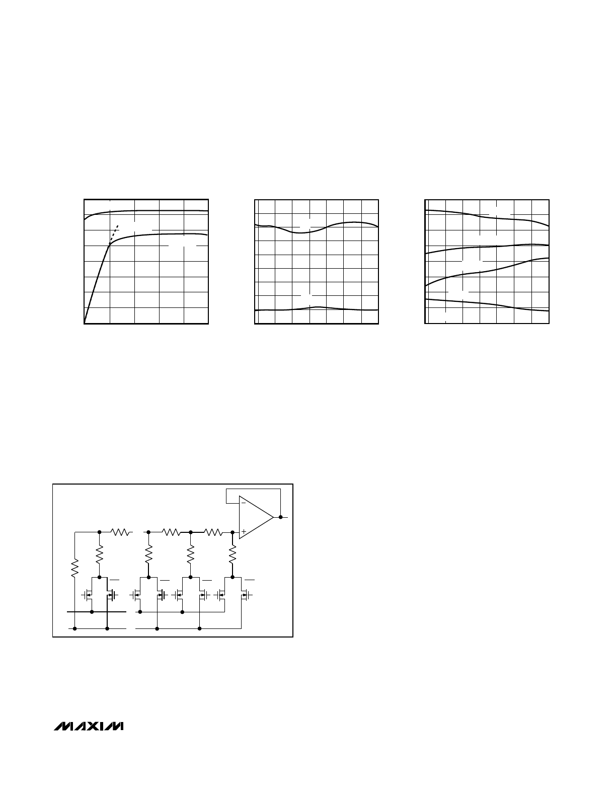
__________________________________________Typical Operating Characteristics
MAX500
CMOS, Quad, Serial-Interface
8-Bit DAC
4
_______________________________________________________________________________________
ELECTRICAL CHARACTERISTICS—Single Supply
(V
DD
= +15V ±5%, V
SS
= AGND = DGND = 0V, V
REF
= 10V, T
A
= T
MIN
to T
MAX
, unless otherwise noted.)
Outputs unloaded
For specified performance
Guaranteed monotonic
T
A
= T
MIN
to T
MAX
V
DD
= 15V ±5%,
V
REF
= 10V
T
A
= +25°C
CONDITIONS
mA
12
I
DD
Positive Supply Current
10
V
14.25
15.75
V
DD
Positive Supply Voltage
µV/°C
±30
Zero-Code Tempco
mV
±30
Zero-Code Error
±20
±20
±15
Bits
8
Resolution
±1/2
LSB
±1
Differential Nonlinearity
LSB
±1
Relative Accuracy
±1
LSB
±2
Total Unadjusted Error
±1/2
UNITS
MIN
TYP
MAX
SYMBOL
PARAMETER
Note 2:
Guaranteed by design. Not production tested.
Note 3:
T
A
= +25°C, V
REF
= 10kHz, 10V peak-to-peak sine wave.
Note 4:
LOAD has a weak internal pull-up resistor to V
DD
.
Note 5:
DAC switched from all 1s to all 0s, and all 0s to all 1s code.
Note 6:
Sample tested at +25°C to ensure compliance.
Note 7:
Slow rise and fall times are allowed on the digital inputs to facilitate the use of opto-couplers. Only timing for SCL is given
because the other digital inputs should be stable when SCL transitions.
MAX500A
MAX500A
T
A
= +25°C
MAX500A
MAX500B
MAX500A
V
REF
= 10V
ppm/°C
±5
Full-Scale Tempco
LSB
±1
Full-Scale Error
MAX500A
MAX500B
MAX500B
MAX500B
MAX500B
T
A
= T
MIN
to T
MAX
STATIC PERFORMANCE
REFERENCE INPUT—
All specifications are the same as for dual supplies.
DIGITAL INPUTS—
All specifications are the same as for dual supplies.
DYNAMIC PERFORMANCE—
All specifications are the same as for dual supplies.
POWER SUPPLIES
SWITCHING CHARACTERISTICS—
All specifications are the same as for dual supplies.
1.0
2
0
0.5
MAX500-04
-0.5
4
0
6
8
10
12
14
V
REF
(V)
-1.0
RELATIVE ACCURACY (LSB)
RELATIVE ACCURACY vs. REFERENCE VOLTAGE
T
A
= +25°C, V
SS
= -5V
V
DD
= 15V
V
DD
= 12V
1.0
2
0
0.5
MAX500-05
-0.5
4
0
6
8
10
12
14
V
REF
(V)
-1.0
DIFFERENTIAL NONLINEARITY (LSB)
DIFFERENTIAL NONLINEARITY vs. REFERENCE VOLTAGE
V
DD
= 15V
T
A
= +25°C, V
SS
= -5V
V
DD
= 12V
MAX500
CMOS, Quad, Serial-Interface
8-Bit DAC
_______________________________________________________________________________________
5
12
0
0
OUTPUT SINK CURRENT
vs. OUTPUT VOLTAGE
2
10
MAX500-01
V
OUT
(V)
I
SINK
(mA)
8
6
4
2
6
10
8
4
14
16
V
SS
= -5V
R
O
≅
200
Ω
V
SS
= 0V
10
-6
SUPPLY CURRENT
vs. TEMPERATURE
-4
6
MAX500-02
TEMPERATURE (°C)
SUPPLY CURRENT (mA)
0
-2
4
2
8
12
-55
125
25
-25
0
75
50
100
I
DD
I
SS
1.5
-2.0
ZERO-CODE ERROR
vs. TEMPERATURE
-1.5
1.0
MAX500-03
TEMPERATURE (°C)
ZERO-CODE ERROR (mV)
0.0
-1.0
0.5
-0.5
2.0
-55
125
25
-25
0
75
50
100
V
SS
= -5V
V
OUT
A
V
OUT
B
V
OUT
C
V
OUT
D
____________________________Typical Operating Characteristics (continued)
_______________Detailed Description
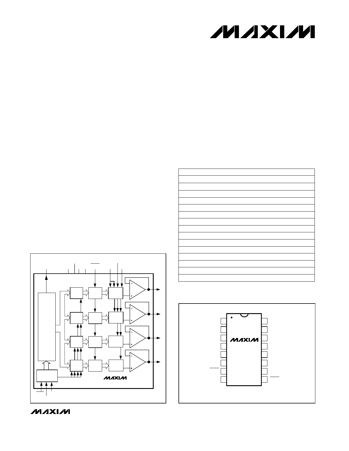
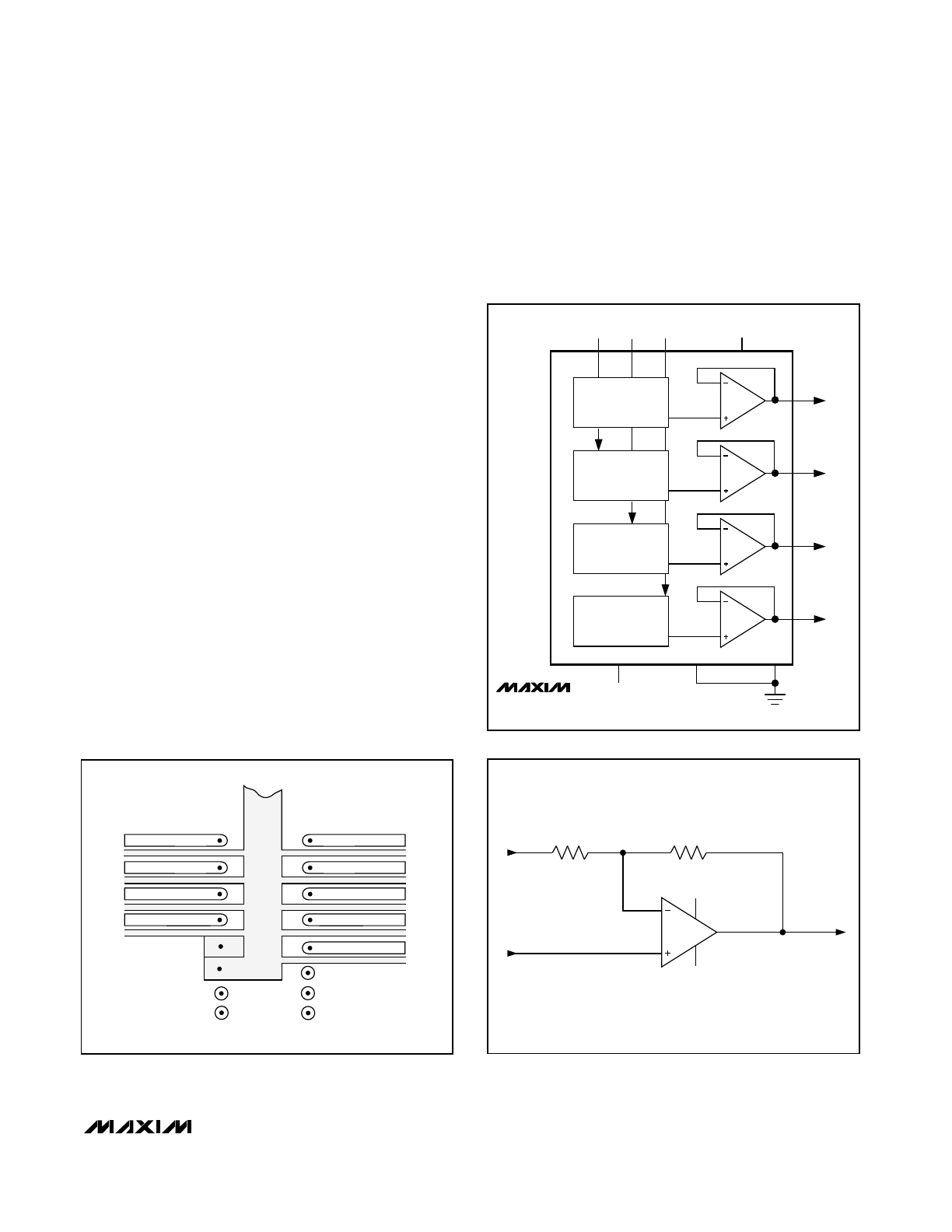
The MAX500 has four matched voltage-output digital-to-
analog converters (DACs). The DACs are “inverted”
R-2R ladder networks which convert 8 digital bits into
equivalent analog output voltages in proportion to the
applied reference voltage(s). Two DACs in the MAX500
have a separate reference input while the other two
DACs share one reference input. A simplified circuit
diagram of one of the four DACs is provided in Figure 1.
V
REF
Input
The voltage at the V
REF
pins (pins 4, 12, and 13) sets
the full-scale output of the DAC. The input impedance
of the V
REF
inputs is code dependent. The lowest
value, approximately 11k
Ω
(5.5k
Ω
for V
REF
A/B), occurs
when the input code is 01010101. The maximum value
of infinity occurs when the input code is 00000000.
Because the input resistance at V
REF
is code depen-
dent, the DAC’s reference sources should have an out-
put impedance of no more than 20
Ω
(no more than
10
Ω
for V
REF
A/B). The input capacitance at V
REF
is
also code dependent and typically varies from 15pF to
35pF (30pF to 70pF for V
REF
A/B). V
OUT
A, V
OUT
B,
V
OUT
C, and V
OUT
D can be represented by a digitally
programmable voltage source as:
V
OUT
= N
b
x V
REF
/ 256
where N
b
is the numeric value of the DAC’s binary
input code.
Output Buffer Amplifiers
All voltage outputs are internally buffered by precision
unity-gain followers, which slew at greater than 3V/µs.
When driving 2k
Ω
in parallel with 100pF with a full-scale
transition (0V to +10V or +10V to 0V), the output settles
to ±1/2LSB in less than 4µs. The buffers will also drive
2k
Ω
in parallel with 500pF to 10V levels without oscilla-
tion. Typical dynamic response and settling perfor-
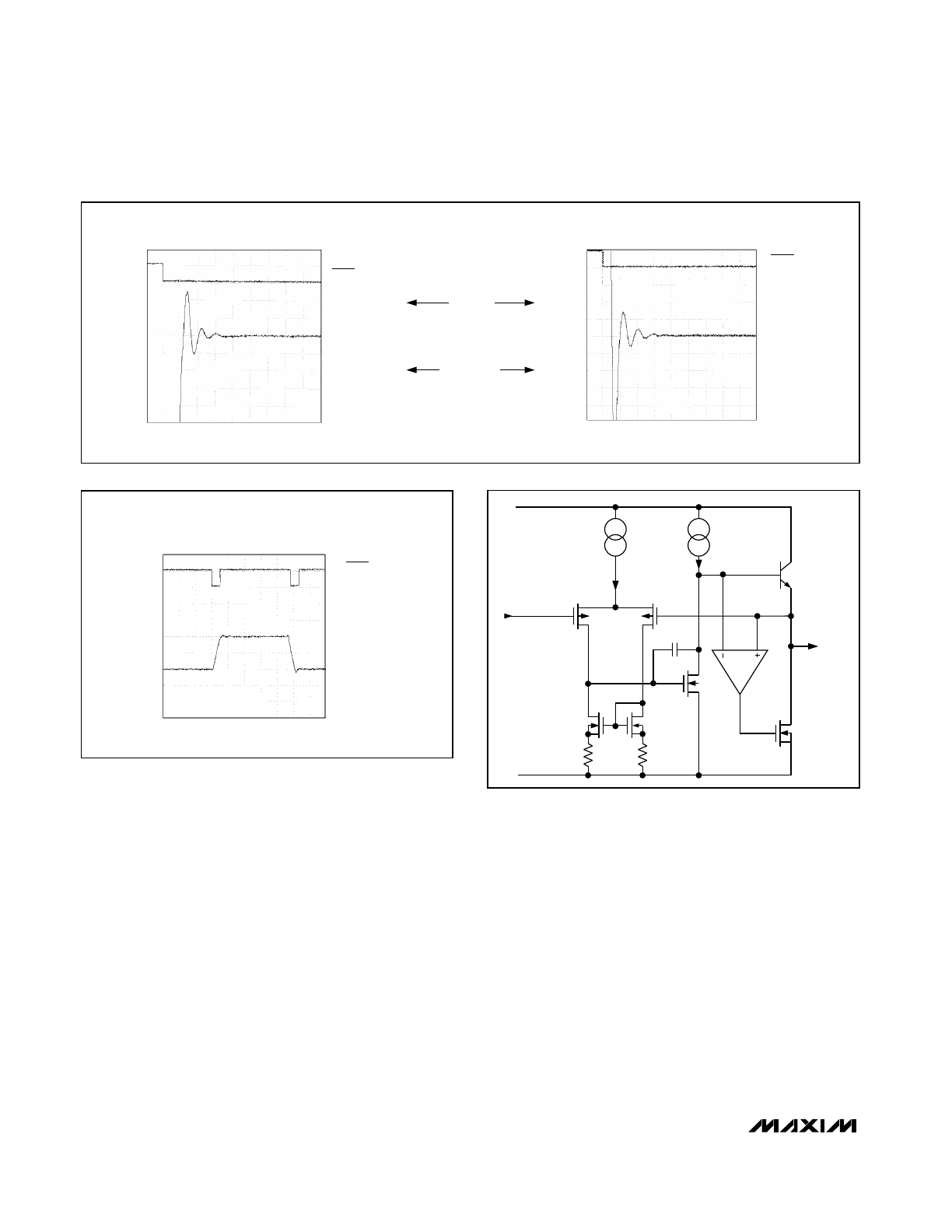
mance of the MAX500 is shown in Figures 2 and 3.
A simplified circuit diagram of an output buffer is
shown in Figure 4. Input common-mode range to
AGND is provided by a PMOS input structure. The out-
put circuitry incorporates a pull-down circuit to actively
drive V
OUT
to within +15mV of the negative supply
(V
SS
). The buffer circuitry allows each DAC output to
R
R
R
2R
2R
2R
2R
2R
V
REF
AGND
V
OUT
DB0
DB5
DB6
DB7
DB0
DB5
DB6
DB7
…
…
…
Figure 1. Simplified DAC Circuit Diagram
MAX500
sink, as well as source up to 5mA. This is especially
important in single-supply applications, where V
SS
is
connected to AGND, so that the zero error is kept at or
under 1/2LSB (V
REF
= +10V). A plot of the Output Sink
Current vs. Output Voltage is shown in the
Typical
Operating Characteristics section.
Digital Inputs
and Interface Logic
The digital inputs are compatible with both TTL and 5V
CMOS logic; however, the power-supply current (I
DD
)
is somewhat dependent on the input logic level. Supply
current is specified for TTL input levels (worst case) but
is reduced (by about 150µA) when the logic inputs are
driven near DGND or 4V above DGND.
Do not drive the digital inputs directly from CMOS logic
running from a power supply exceeding 5V. When driv-
ing SCL through an opto-isolator, use a Schmitt trigger
to ensure fast SCL rise and fall times.
The MAX500 allows the user to choose between a
3-wire serial interface and a 2-wire serial interface.
The choice between the 2-wire and the 3-wire inter-
face is set by the
LOAD signal. If the LOAD is allowed
to float (it has a weak internal pull-up resistor to V
DD
),
the 2-wire interface is selected. If the
LOAD signal is
kept to a TTL-logic high level, the 3-wire interface
is selected.
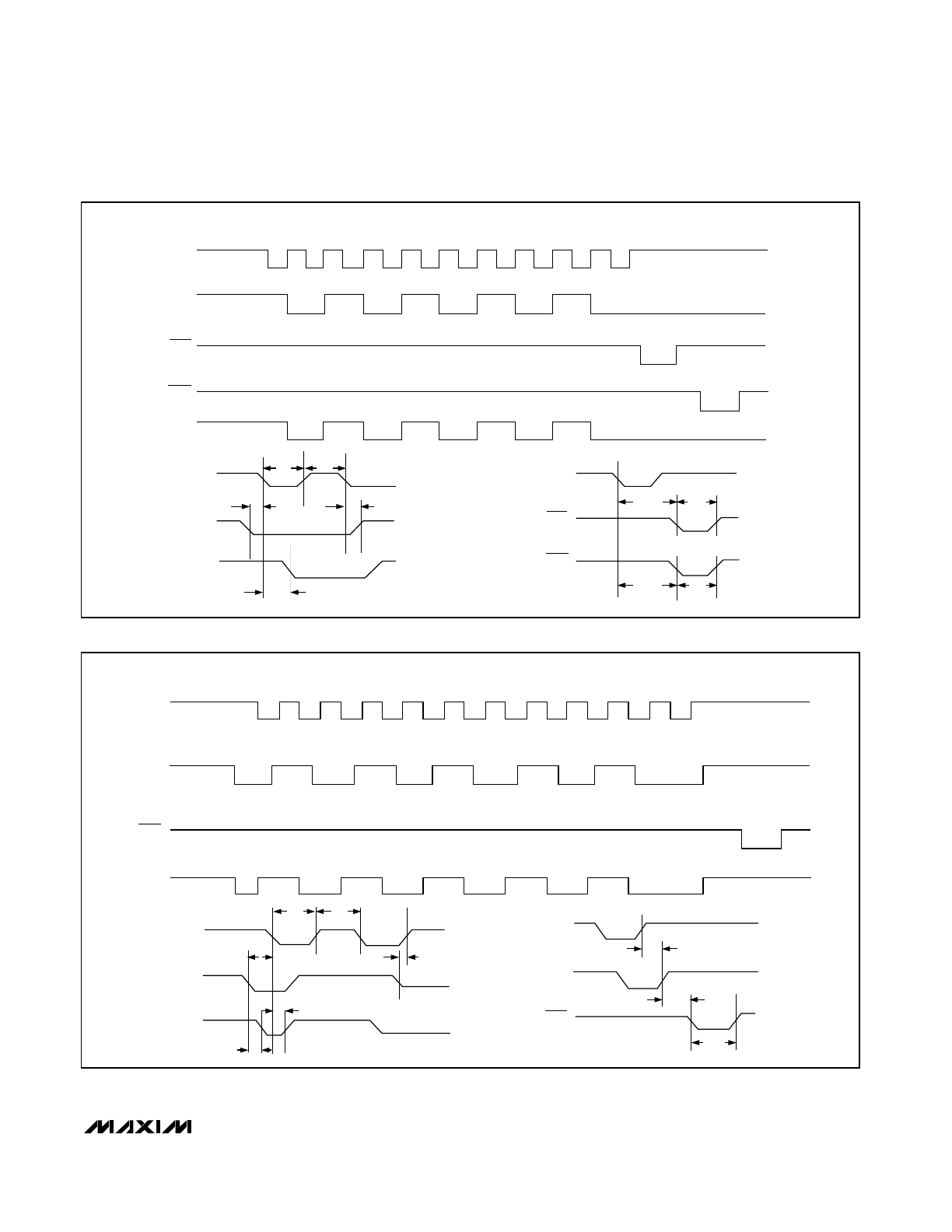
3-Wire Interface
The 3-wire interface uses the classic Serial Data (SDA),
Serial Clock (SCL), and
LOAD signals that are used
in standard shift registers. The data is clocked in on
the falling edge of SCL until all 10 bits (8 data bits and
2 address bits) are entered into the shift register.
CMOS, Quad, Serial-Interface
8-Bit DAC
6
_______________________________________________________________________________________
INPUT
(5V/div)
OUTPUT
(20mV/div)
DYNAMIC RESPONSE
(V
SS
= -5V or 0V)
2
µ
s/div
LDAC
5V/div
OUTPUT
5V/div
V
SS
V
DD
PMOS
(+)
FROM
INVERTED
DAC
OUTPUT
INPUTS
C
C
(-)
NPN
EMITTER
FOLLOWER
PULL-UP
V
OUT
NMOS
ACTIVE
PULL-DOWN
CIRCUIT
Figure 2. Positive and Negative Settling Times
Figure 3. Dynamic Response
Figure 4. Simplified Output Buffer Circuit
POSITIVE STEP
(V
SS
= -5V or 0V)
1
µ
s/div
LDAC
5V/div
OUTPUT
100mV/div
NEGATIVE STEP
(V
SS
= -5V or 0V)
1
µ
s/div
LDAC
5V/div
OUTPUT
100mV/div
MAX500
CMOS, Quad, Serial-Interface
8-Bit DAC
_______________________________________________________________________________________
7
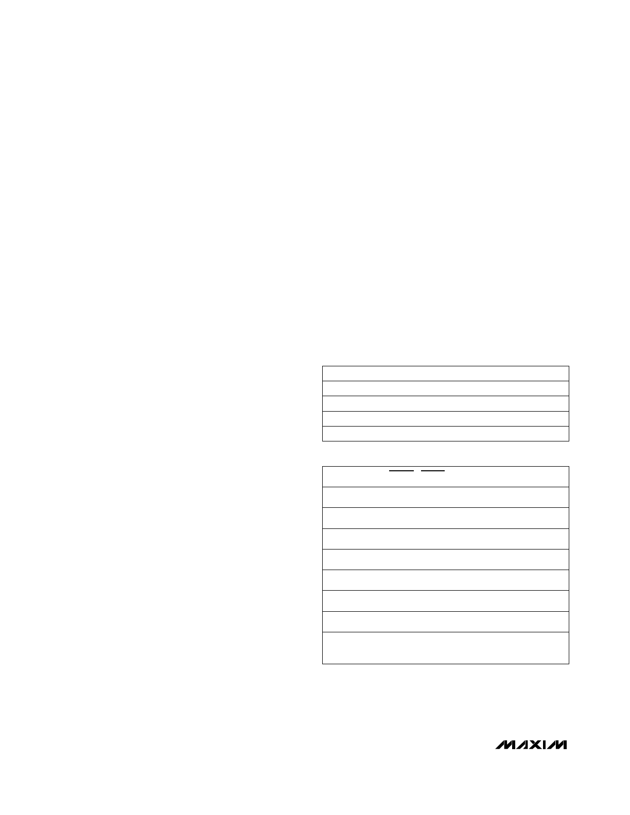
SCL
LOAD
LDAC
t
LDS
t
LDW
t
LDS
t
LDAC
SCL
SDA
SRO
t
2
t
1
t
S1
t
H
t
D1
SCL
SDA
LOAD
LDAC
SRO
(SERIAL OUTPUT)
A1
A0
D7
MSB
D6
D5
D4
D3
D2
D1
D0
LSB
A1
A0
D7
MSB
D6
D5
D4
D3
D2
D1
D0
LSB
SDA
LDAC
SCL
SDA
SRO
SCL
SDA
LDAC
SRO
(SERIAL OUTPUT)
SCL
t
2
t
1
t
S1
t
S3
t
D1
t
D1
t
S2
t
LDS
t
LDAC
Figure 5. 3-Wire Mode
Figure 6. 2-Wire Mode
MAX500
A low level on
LOAD line initiates the transfer of data
from the shift register to the addressed input register.
The data can stay in this register until all four of the
input registers are updated. Then all of the DAC regis-
ters can be simultaneously updated using the
LDAC
(load DAC) signal. When
LDAC is low, the input regis-
ter’s data is loaded into the DAC registers (see Figure 5
for timing diagram). This mode is cascadable by con-
necting Serial Output (SRO) to the second chip’s SDA
pin. The delay of the SRO pin from SCL does not cause
setup/hold time violations, no matter how many
MAX500s are cascaded. Restrict the voltage at
LDAC
and
LOAD to +5.5V for a logic high.
2-Wire Interface
The 2-wire interface uses SDA and SCL only.
LOAD
must be floating or tied to V
DD
. Each data frame (8 data
bits and 2 address bits) is synchronized by a timing
relationship between SDA and SCL (see Figure 6 for
the timing diagram). Both SDA and SCL should normal-
ly be high when inactive. A falling edge of SDA (while
SCL is high) followed by a falling edge of SCL (while
SDA is low) is the start condition. This always loads a 0
into the first bit of the shift register. The shift register is
extended to 11 bits so this “data” will not affect the
input register information. The timing now follows the 3-
wire interface, except the SDA line is not allowed to
change when SCL is high (this prevents the MAX500
from retriggering its start condition). After the last data
bit is entered, the SDA line should go low (while the
SCL line is low), then the SCL line should rise followed
by the SDA line rising. This is defined as the stop con-
dition, or end of frame.
Cascading the 2-wire interface can be done, but the
user must be careful of both timing and formatting.
Timing must take into account the intrinsic delay of the
SRO pin from the internally generated start/stop condi-
tions. The t
S2
value should be increased by n times t
D1
(where n = number of cascaded MAX500s). The t
LDS
value should also be increased by n times t
D1
. No other
timing parameters need to be modified. A more serious
concern is one of formatting. Generally, since each
frame has a start/stop condition, each chip that has
data cascaded through it will accept that data as if it
were its own data. Therefore, to circumvent this limita-
tion, the user should not generate a stop bit until all
DACs have been loaded. For example, if there are
three MAX500s cascaded in the 2-wire mode, the data
transfer should begin with a start condition, followed by
10 data bits, a zero bit, 10 data bits, a zero bit, 10 data
bits, and then a stop condition. This will prevent each
MAX500 from decoding the middle data for itself.
The data is entered into the shift register in the follow-
ing order:
A1 A0 D7 D6 D5 D4 D3 D2 D1 D0
(First) (MSB) (Last)
where address bits A1 and A0 select which DAC regis-
ter receives data from the internal shift register. Table 1
lists the channel addresses. D7 (MSB) through D0 is
the data byte.
Since
LDAC is asynchronous with respect to SCL, SDA,
and
LOAD, care must be taken to assure that incorrect
data is not latched through to the DAC registers. If the
3-wire serial interface is used,
LDAC can be either tied
low permanently or tied to
LOAD as long as t
LDS
is
always maintained. However, if the 2-wire interface is
used,
LDAC should not fall before the stop condition is
internally detected. (This is the reason for the t
LDS
delay of
LDAC after the last rising edge of SDA.)
CMOS, Quad, Serial-Interface
8-Bit DAC
8
_______________________________________________________________________________________
A1
A0
SELECTED INPUT REGISTER
L
L
DAC A Input Register
L
H
DAC B Input Register
H
L
DAC C Input Register
H
H
DAC D Input Register
SCL
SDA
LOAD LDAC
FUNCTION
F
Data
V
DD
H
Latching data into
shift register (2W)
H
Data
V
DD
H
Data should not be
changing (2W)
L
X
V
DD
H
Data is allowed to
change (2W)
F
Data
M
H
Latching data into
shift register (3W)
H
X
M
H
Data is allowed to
change (3W)
L
X
M
H
Data is allowed to
change (3W)
H
X
L
H
Loads input register
from shift register (3W)
H
X
L
L
DAC register reflects
data held in their respective
input registers
Notes:
H = Logic High
2W = 2-Wire
L = Logic Low
3W = 3-Wire
M = TTL Logic High
F = Falling Edge
X = Don’t Care
Table 1. DAC Addressing
Table 2. Logic Input Truth Table
The SRO output swings from V
DD
to DGND. Cascading
to other MAX500s poses no problem. If SRO is used to
drive a TTL-compatible input, use a clamp diode
between TTL +5V and V
DD
and the current-limiting
resistor to prevent potential latchup problems with
the 5V supply.
Table 2 shows the truth table for SDA, SCL,
LOAD, and
LDAC operation. Figures 5 and 6 show the timing dia-
grams for the MAX500.
__________Applications Information
Power-Supply and Reference
Operating Ranges
The MAX500 is fully specified to operate with V
DD
between +12V ±5% and +15V ±10% (+11.4V to
+16.5V), and with V
SS
from 0V to -5.5V. 8-bit perfor-
mance is also guaranteed for single-supply operation
(V
SS
= 0V), however, zero-code error is reduced when
V
SS
is -5V (see
Output Buffer Amplifiers section).
For an adequate DAC and buffer operating range, the
V
REF
voltage must always be at least 4V below V
DD
.
The MAX500 is specified to operate with a reference
input range of +2V to V
DD
- 4V.
Ground Management
Digital or AC transient signals between AGND and
DGND will create noise at the analog outputs. It is rec-
ommended that AGND and DGND be tied together at
the DAC and that this point be tied to the highest quali-
ty ground available. If separate ground buses are used,
then two clamp diodes (1N914 or equivalent) should be
connected between AGND and DGND to keep the two
ground buses within one diode drop of each other. To
avoid parasitic device turn-on, AGND must not be
allowed to be more negative than DGND. DGND should
be used as supply ground for bypassing purposes.
MAX500
CMOS, Quad, Serial-Interface
8-Bit DAC
_______________________________________________________________________________________
9
Figure 7. Suggested MAX500 PC Board Layout for
Minimizing Crosstalk
Figure 8. MAX500 Unipolar Output Circuit
COMPONENT SIDE (TOP VIEW)
V
OUT
C
V
OUT
D
V
DD
V
REF
C
V
REF
D
SYSTEM GND
V
OUT
B
V
OUT
A
V
SS
V
REF
A/B
AGND
DGND
V
REF
D
DAC A
DAC B
DAC C
DAC D
V
REF
C
V
REF
A/B
MAX500
V
OUT
A
V
OUT
B
V
OUT
C
V
OUT
D
DIGITAL
INPUTS
NOT
SHOWN
REFERENCE INPUTS
2
1
16
15
V
DD
+15V
13
12
4
14
3
-5V (OR GND)
5
6
V
SS
AGND
DGND
V
REF
DAC
OUTPUT
FROM MAX500
R1
R2
+15V
-15V
R1 = R2 = 10k
Ω
±0.1%
NOTE: V
REF
IS THE REFERENCE INPUT FOR THE MAX500
V
OUT
Figure 9. Bipolar Output Circuit
MAX500
Careful PC board ground layout techniques should be
used to minimize crosstalk between DAC outputs, the
reference input(s), and the digital inputs. This is partic-
ularly important if the reference is driven from an AC
source. Figure 7 shows suggested PC board layouts for
minimizing crosstalk.
Unipolar Output
In unipolar operation, the output voltages and the refer-
ence input(s) are the same polarity. The unipolar circuit
configuration is shown in Figure 8 for the MAX500. The
device can be operated from a single supply with a
slight increase in zero error (see
Output Buffer
Amplifiers section). To avoid parasitic device turn-on,
the voltage at V
REF
must always be positive with
respect to AGND. The unipolar code table is given in
Table 3.
Bipolar Output
Each DAC output may be configured for bipolar opera-
tion using the circuit in Figure 9. One op amp and two
resistors are required per channel. With R1 = R2:
V
OUT
= V
REF
(2D
A
- 1)
where D
A
is a fractional representation of the digital
word in Register A.
Table 4 shows the digital code versus output voltage
for the circuit in Figure 9.
Offsetting AGND
AGND can be biased above DGND to provide an arbi-
trary nonzero output voltage for a “zero” input code. This
is shown in Figure 10. The output voltage at V
OUT
A is:
V
OUT
A = V
BIAS
+ D
A
V
IN
where D
A
is a fractional representation of the digital
input word. Since AGND is common to all four DACs,
all outputs will be offset by V
BIAS
in the same manner.
Since AGND current is a function of the four DAC
codes, it should be driven by a low-impedance source.
V
BIAS
must be positive.
CMOS, Quad, Serial-Interface
8-Bit DAC
10
______________________________________________________________________________________
DAC A
MAX500
4
14
AGND
2
V
OUT
A
DGND
V
SS
V
REF
A/B
V
DD
3
6
+
V
IN
-
+
V
BIAS
-
5
+15V
-5V (OR GND)
DIGITAL INPUTS NOT SHOWN
Figure 10. AGND Bias Circuit
Table 3. Unipolar Code Table
Table 4. Bipolar Code Table
1 0 0 0
DAC CONTENTS
0 0 0 1
MSB
LSB
ANALOG
OUTPUT
1 1 1 1
1 1 1 1
127
+V
REF
(
––––
)
128
1
+V
REF
(
––––
)
128
1 0 0 0
0 0 0 0
0V
0 1 1 1
1 1 1 1
1
-V
REF
(
––––
)
128
0 0 0 0
0 0 0 0
128
-V
REF
(
––––
)
= -V
REF
128
0 0 0 0
0 0 0 1
127
-V
REF
(
––––
)
128
1 0 0 0
DAC CONTENTS
0 0 0 1
MSB
LSB
ANALOG
OUTPUT
1 1 1 1
1 1 1 1
255
+V
REF
(
––––
)
256
129
+V
REF
(
––––
)
256
1 0 0 0
0 0 0 0
128 V
REF
+V
REF
(
––––
)
= +
––––
256 2
0 1 1 1
1 1 1 1
127
+V
REF
(
––––
)
256
0 0 0 0
0 0 0 0
0V
0 0 0 0
0 0 0 1
1
+V
REF
(
––––
)
256
1
Note:
1LSB = (V
REF
) (2
-8
) = +V
REF
(
–––
)
256
1
Note:
1LSB = (V
REF
) (2
-8
) = +V
REF
(
–––
)
256
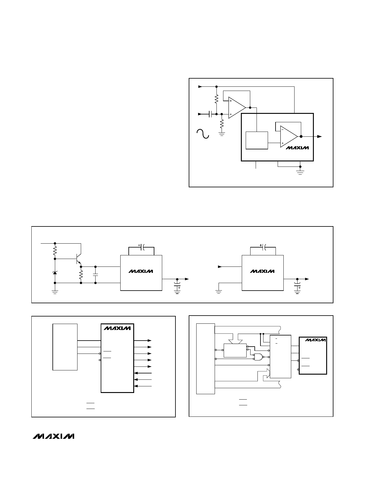
Using an AC Reference
In applications where V
REF
has AC signal components,
the MAX500 has multiplying capability within the limits
of the V
REF
input range specifications. Figure 11 shows
a technique for applying a sine-wave signal to the refer-
ence input, where the AC signal is biased up before
being applied to V
REF
. Output distortion is typically less
than 0.1% with input frequencies up to 50kHz, and the
typical -3dB frequency is 700kHz. Note that V
REF
must
never be more negative than AGND.
Generating V
SS
The performance of the MAX500 is specified for both
dual and single-supply (V
SS
= 0V) operation. When the
improved performance of dual-supply operation is
desired, but only a single supply is available, a -5V V
SS
supply can be generated using an ICL7660 in one of
the circuits of Figure 12.
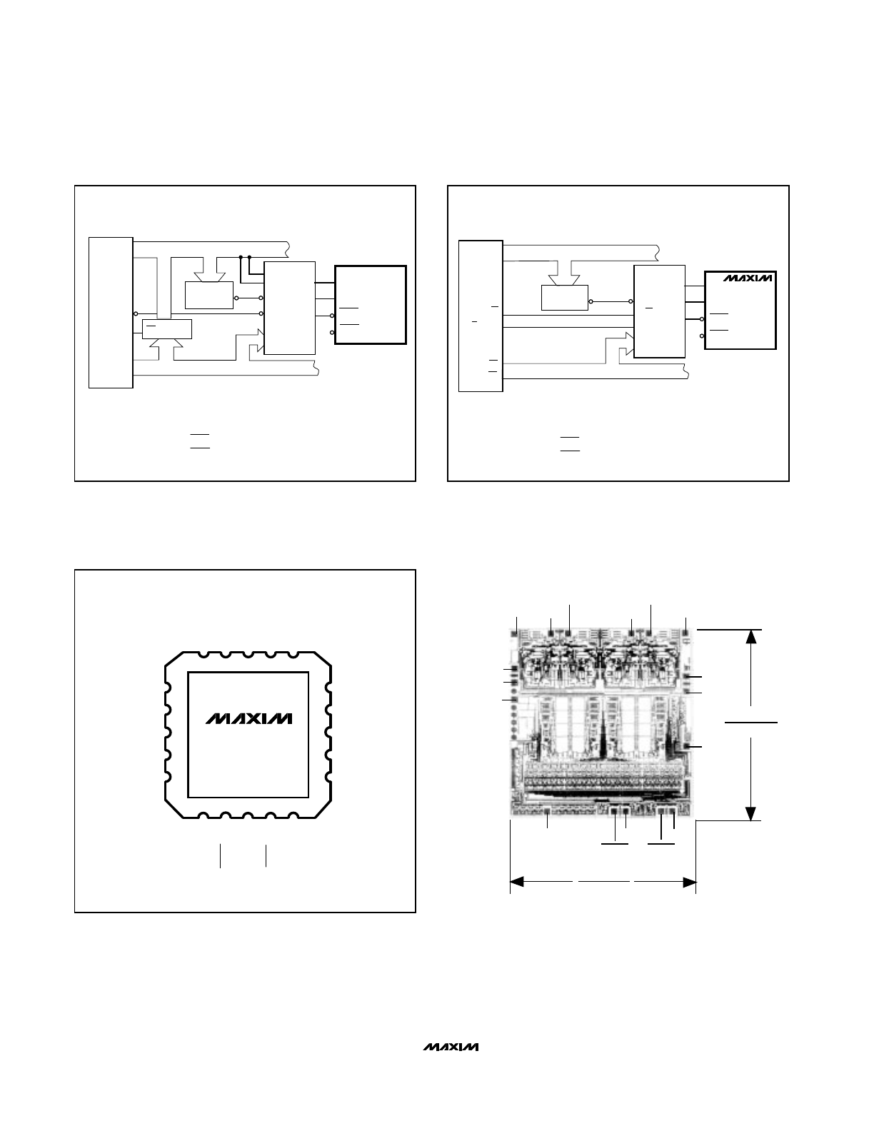
Digital Interface Applications
Figures 13 through 16 show examples of interfacing the
MAX500 to most popular microprocessors.
MAX500
CMOS, Quad, Serial-Interface
8-Bit DAC
______________________________________________________________________________________
11
DAC B
MAX500
4
14
1 V
OUT
B
DGND
V
SS
V
REF
A/B
V
DD
3
6
-5V (OR GND)
DIGITAL INPUTS NOT SHOWN
AGND
V
OUT
B
+4V
-4V
AC
REFERENCE
INPUT
+15V
15k
10k
5
ICL7660
CAP+
CAP-
V+
GND
V
OUT
ICL7660
CAP+
CAP-
V+
GND
V
OUT
6V
ZENER
12V to 15V
10k
2N2222
10k
10
µ
F
8
3
2
10
µ
F
4
5
-5V
V
SS
OUT
10
µ
F
+5V
LOGIC
SUPPLY
-5V
V
SS
OUT
10
µ
F
8
3
4
5
10
µ
F
2
SCL
SDA
LDAC
LOAD*
80C51
P1.0
P1.1
P1.2
P1.3
CONNECT LOAD TO P1.3 FOR 3-WIRE MODE OR
CONNECT LOAD TO V
DD
FOR 2-WIRE MODE
. . . . . . .
SRO
V
OUT
A
V
OUT
B
V
OUT
C
V
OUT
D
V
REF
A/B
V
REF
C
V
REF
D
MAX500
*
ADDRESS BUS
EN ADDRESS
CODE
B/A
DATA BUS
CONNECT LOAD TO P1.3 FOR 3-WIRE MODE OR
CONNECT LOAD TO V
DD
FOR 2-WIRE MODE
C/D
CE
RD
INT
D7
D0
Z8420
B0
B1
B2
B3
A15
A0
Z80
I/O REQ
WR
INT
D7
D0
A1
A0
SCL
SDA
LDAC
LOAD*
. .
MAX500
*
Figure 11. AC Reference Input Circuit
Figure 12. Generating -5V for V
SS
Figure 14. Z-80 with Z8420 PIO Interface
Figure 13. 80C51 Interface
Maxim cannot assume responsibility for use of any circuitry other than circuitry entirely embodied in a Maxim product. No circuit patent licenses are
implied. Maxim reserves the right to change the circuitry and specifications without notice at any time.
12
__________________Maxim Integrated Products, 120 San Gabriel Drive, Sunnyvale, CA 94086 (408) 737-7600
© 1996 Maxim Integrated Products
Printed USA
is a registered trademark of Maxim Integrated Products.
MAX500
CMOS, Quad, Serial-Interface,
8-Bit DAC
___________________Chip Topography
____Pin Configurations (continued)
CONNECT LOAD TO P1.3 FOR 3-WIRE MODE OR
CONNECT LOAD TO V
DD
FOR 2-WIRE MODE
*
A15
A8
8085/
8088
WR
ALE
AD7
AD0
EN LATCH
ADDRESS BUS
ADDRESS
DECODE
ADDRESS AND DATA BUS
A0
CS
WR
D7
D0
SCL
SDA
LDAC
LOAD*
82C55
PA0
PA1
PA2
PA3
MAX500
. .
A1
CONNECT LOAD TO P1.3 FOR 3-WIRE MODE OR
CONNECT LOAD TO V
DD
FOR 2-WIRE MODE
*
A15
A0
6809/
6502
R/W
Θ
OR E
∆
7
D0
ADDRESS BUS
ADDRESS
DECODE
DATA BUS
C32
R/W
DB7
DB0
6821
6521 PA0
PA1
PA2
PA3 . .
E
SCL
SDA
LDAC
LOAD*
MAX500
Figure 15. 8085/8088 with Programmable Peripheral Interface
Figure 16. 6809/6502 Interface
V
REF
C
SRO
V
REF
D
V
REF
B
AGND
V
REF
A
Vss V
OUT
A
V
OUT
B
V
DD
SCL
LOAD
LDAC
DGND
SDA
0.159"
(4.039mm)
0.150"
(3.810mm)
V
OUT
C
V
OUT
D
14
15
16
17
18
4
5
6
7
8
3
2
1
20
19
9
10
11
12
13
MAX500
V
SS
V
REF
A/B
AGND
N.C.
N.C.
V
DD
V
REF
C
V
REF
D
SRO
N.C.
V
OUT
A
V
OUT
B
N.C.
V
OUT
C
V
OUT
D
DGND
LDAC
SDA
LOAD
SCL
LCC
TOP VIEW