
_______________General Description
The MAX202E–MAX213E, MAX232E/MAX241E line
drivers/receivers are designed for RS-232 and V.28
communications in harsh environments. Each
transmitter output and receiver input is protected
against ±15kV electrostatic discharge (ESD) shocks,
without latchup. The various combinations of features
are outlined in the
Selection Guide. The drivers and
receivers for all ten devices meet all EIA/TIA-232E and
CCITT V.28 specifications at data rates up to 120kbps,
when loaded in accordance with the EIA/TIA-232E
specification.
The MAX211E/MAX213E/MAX241E are available in 28-
pin SO packages, as well as a 28-pin SSOP that uses
60% less board space. The MAX202E/MAX232E come
in 16-pin narrow SO, wide SO, and DIP packages. The
MAX203E comes in a 20-pin DIP/SO package, and
needs no external charge-pump capacitors. The
MAX205E comes in a 24-pin wide DIP package, and
also eliminates external charge-pump capacitors. The
MAX206E/MAX207E/MAX208E come in 24-pin SO,
SSOP, and narrow DIP packages. The MAX232E/
MAX241E operate with four 1µF capacitors, while the
MAX202E/MAX206E/MAX207E/MAX208E/MAX211E/
MAX213E operate with four 0.1µF capacitors, further
reducing cost and board space.
________________________Applications
Notebook, Subnotebook, and Palmtop Computers
Battery-Powered Equipment
Hand-Held Equipment
____________________________Features
♦
ESD Protection for RS-232 I/O Pins:
±15kV—Human Body Model
±8kV—IEC1000-4-2, Contact Discharge
±15kV—IEC1000-4-2, Air-Gap Discharge
♦
Latchup Free (unlike bipolar equivalents)
♦
Guaranteed 120kbps Data Rate—LapLink™
Compatible
♦
Guaranteed 3V/µs Min Slew Rate
♦
Operate from a Single +5V Power Supply
MAX202E–MAX213E, MAX232E/MAX241E
±15kV ESD-Protected, +5V RS-232 Transceivers
________________________________________________________________
Maxim Integrated Products
1
16
15
14
13
12
11
10
9
1
2
3
4
5
6
7
8
V
CC
GND
T1OUT
R1IN
C2+
C1-
V+
C1+
TOP VIEW
MAX202E
MAX232E
R1OUT
T1IN
T2IN
R2OUT
R2IN
T2OUT
V-
C2-
DIP/SO
_________________Pin Configurations
_____________________________________________________________Selection Guide
19-0175; Rev 3; 5/96
LapLink is a registered trademark of Traveling Software, Inc.
Pin Configurations and Typical Operating Circuits continued at
end of data sheet.
Ordering Information appears at end of data sheet.
For free samples & the latest literature: http://www.maxim-ic.com, or phone 1-800-998-8800
Yes
PART
No. of RS-232
DRIVERS
No. of RS-232
RECEIVERS
RECEIVERS
ACTIVE IN
SHUTDOWN
No. of
EXTERNAL
CAPACITORS
LOW-POWER
SHUTDOWN
TTL THREE-
STATE
MAX202E
2
2
0
4 (0.1µF)
No
No
MAX203E
2
2
0
None
No
No
MAX205E
5
5
0
None
Yes
Yes
MAX206E
4
3
0
4 (0.1µF)
Yes
Yes
MAX207E
5
3
0
4 (0.1µF)
No
No
MAX208E
4
4
0
4 (0.1µF)
No
No
MAX211E
4
5
0
4 (0.1µF)
Yes
Yes
MAX213E
4
5
2
4 (0.1µF)
Yes
Yes
MAX232E
2
2
0
4 (1µF)
No
No
MAX241E
4
5
0
4 (1µF)
Yes
MAX202E–MAX213E, MAX232E/MAX241E
±15kV ESD-Protected, +5V RS-232 Transceivers
2
_______________________________________________________________________________________
ABSOLUTE MAXIMUM RATINGS
V
CC
...........................................................................-0.3V to +6V
V+ ................................................................(V
CC
- 0.3V) to +14V
V- ............................................................................-14V to +0.3V
Input Voltages
T_IN ............................................................-0.3V to (V+ + 0.3V)
R_IN ...................................................................................±30V
Output Voltages
T_OUT.................................................(V- - 0.3V) to (V+ + 0.3V)
R_OUT ......................................................-0.3V to (V
CC
+ 0.3V)
Short-Circuit Duration, T_OUT....................................Continuous
Continuous Power Dissipation (T
A
= +70°C)
16-Pin Plastic DIP (derate 10.53mW/°C above +70°C)....842mW
16-Pin Narrow SO (derate 8.70mW/°C above +70°C) .....696mW
16-Pin Wide SO (derate 9.52mW/°C above +70°C) ......762mW
20-Pin Plastic DIP (derate 11.11mW/°C above +70°C)...889mW
20-Pin SO (derate 10.00mW/°C above +70°C).............800mW
24-Pin Narrow Plastic DIP
(derate 13.33mW/°C above +70°C) ...............................1.07W
24-Pin Wide Plastic DIP
(derate 14.29mW/°C above +70°C) ................................1.14W
24-Pin SO (derate 11.76mW/°C above +70°C).............941mW
24-Pin SSOP (derate 8.00mW/°C above +70°C) ..........640mW
28-Pin SO (derate 12.50mW/°C above +70°C)....................1W
28-Pin SSOP (derate 9.52mW/°C above +70°C) ..........762mW
Operating Temperature Ranges
MAX2_ _EC_ _ .....................................................0°C to +70°C
MAX2_ _EE_ _...................................................-40°C to +85°C
Storage Temperature Range .............................-65°C to +165°C
Lead Temperature (soldering, 10sec) .............................+300°C
ELECTRICAL CHARACTERISTICS
(V
CC
= +5V ±10% for MAX202E/206E/208E/211E/213E/232E/241E; V
CC
= +5V ±5% for MAX203E/205E/207E; C1–C4 = 0.1µF for
MAX202E/206E/207E/208E/211E/213E; C1–C4 = 1µF for MAX232E/241E; T
A
= T
MIN
to T
MAX
; unless otherwise noted. Typical values
are at T
A
= +25°C.)
Stresses beyond those listed under “Absolute Maximum Ratings” may cause permanent damage to the device. These are stress ratings only, and functional
operation of the device at these or any other conditions beyond those indicated in the operational sections of the specifications is not implied. Exposure to
absolute maximum rating conditions for extended periods may affect device reliability.
R_OUT; I
OUT
= -1.0mA
V
3.5 V
CC
- 0.4
Output Voltage High
V
OH
EN = V
CC
, EN = 0V, 0V
≤
R
OUT
≤
V
CC
,
MAX205E–208E/211E/213E/241E outputs disabled
µA
±0.05
±10
Output Leakage Current
R_OUT; I
OUT
= 3.2mA (MAX202E/203E/232E) or
I
OUT
= 1.6mA (MAX205E/208E/211E/213E/241E)
V
0.4
Output Voltage Low
V
OL
T_IN; EN,
SHDN (MAX213E) or
EN, SHDN (MAX205E–208E/211E/241E)
V
0.8
Input Threshold Low
V
IL
8
15
T_IN = 0V (MAX205E–208E/211E/213E/241E)
µA
15
200
Input Pull-Up Current
PARAMETER
CONDITIONS
SYMBOL
UNITS
MIN
TYP
MAX
V
CC
Supply Current
I
CC
mA
11
20
No load, T
A
= +25°C
14
20
5
10
MAX211E/213E
MAX232E
7
15
MAX241E
MAX205E–208E
EN,
SHDN (MAX213E) or EN, SHDN
(MAX205E–208E/211E/241E)
2.4
T_IN
V
2.0
Input Threshold High
V
IH
MAX205E/206E
1
10
1
10
MAX211E/241E
T_IN = 0V to V
CC
(MAX202E/203E/232E)
µA
±10
Input Leakage Current
MAX202E/203E
15
50
MAX213E
DC CHARACTERISTICS
LOGIC
Shutdown Supply Current
T
A
= +25°C, Figure 1
µA
MAX202E–MAX213E, MAX232E/MAX241E
±15kV ESD-Protected, +5V RS-232 Transceivers
_______________________________________________________________________________________
3
ELECTRICAL CHARACTERISTICS (continued)
(V
CC
= +5V ±10% for MAX202E/206E/208E/211E/213E/232E/241E; V
CC
= +5V ±5% for MAX203E/205E/207E; C1–C4 = 0.1µF for
MAX202E/206E/207E/208E/211E/213E; C1–C4 = 1µF for MAX232E/241E; T
A
= T
MIN
to T
MAX
; unless otherwise noted. Typical values
are at T
A
= +25°C.)
Note 1:
MAX211EE_ _ and MAX213EE_ _ tested with V
CC
= +5V ±5%.
MAX205E/206E/211E/213E/241E normal
operation, Figure 2
MAX205E/206E/211E/213E/241E normal
operation, Figure 2
C
L
= 150pF
R
L
= 3k
Ω
to 7k
Ω
, C
L
= 50pF to 1000pF,
one transmitter switching
All drivers loaded with 3k
Ω
to ground (Note 1)
T
A
= +25°C, V
CC
= 5V
V
CC
= 5V, no hysteresis in shutdown
T
A
= +25°C,
V
CC
= 5V
T
A
= +25°C,
V
CC
= 5V
V
CC
= V+ = V- = 0V, V
OUT
= ±2V
CONDITIONS
ns
200
Receiver Output Disable Time
ns
600
Receiver Output Enable Time
µs
4
40
t
PLHR
,
t
PHLR
Receiver Propagation Delay
0.5
10
kbps
120
Maximum Data Rate
mA
±10
±60
Output Short-Circuit Current
Ω
300
Output Resistance
V
-30
30
Input Voltage Range
V
±5
±9
Output Voltage Swing
k
Ω
3
5
7
Input Resistance
V
0.2
0.5
1.0
Input Hysteresis
V
Input Threshold Low
1.7
2.4
V
1.5
2.4
Input Threshold High
UNITS
MIN
TYP
MAX
SYMBOL
PARAMETER
All parts, normal operation
All parts, normal operation
MAX213E (R4, R5),
SHDN = 0V, EN = V
CC
R
L
= 3k
Ω
, C
L
= 2500pF, all transmitters loaded
µs
2
t
PLHT
,
t
PHLT
Transmitter Propagation Delay
T
A
= +25°C, V
CC
= 5V, R
L
= 3k
Ω
to 7k
Ω
,
C
L
= 50pF to 1000pF, measured from -3V to
+3V or +3V to -3V, Figure 3
V/µs
3
6
30
Transition-Region Slew Rate
Human Body Model
±15
IEC1000-4-2, Air-Gap Discharge
kV
±15
ESD-Protection Voltage
IEC1000-4-2, Contact Discharge
±8
All parts, normal operation
MAX213E (R4, R5),
SHDN = 0V, EN = V
CC
0.8
1.2
ESD PERFORMANCE: TRANSMITTER OUTPUTS, RECEIVER INPUTS
TIMING CHARACTERISTICS
EIA/TIA-232E TRANSMITTER OUTPUTS
EIA/TIA-232E RECEIVER INPUTS
MAX213E,
SHDN = 0V,
EN = V
CC
0.6
1.5
Note 1:
MAX211EE_ _ tested with V
CC
= +5V ±5%.
MAX202E–MAX213E, MAX232E/MAX241E
±15kV ESD-Protected, +5V RS-232 Transceivers
4
_______________________________________________________________________________________
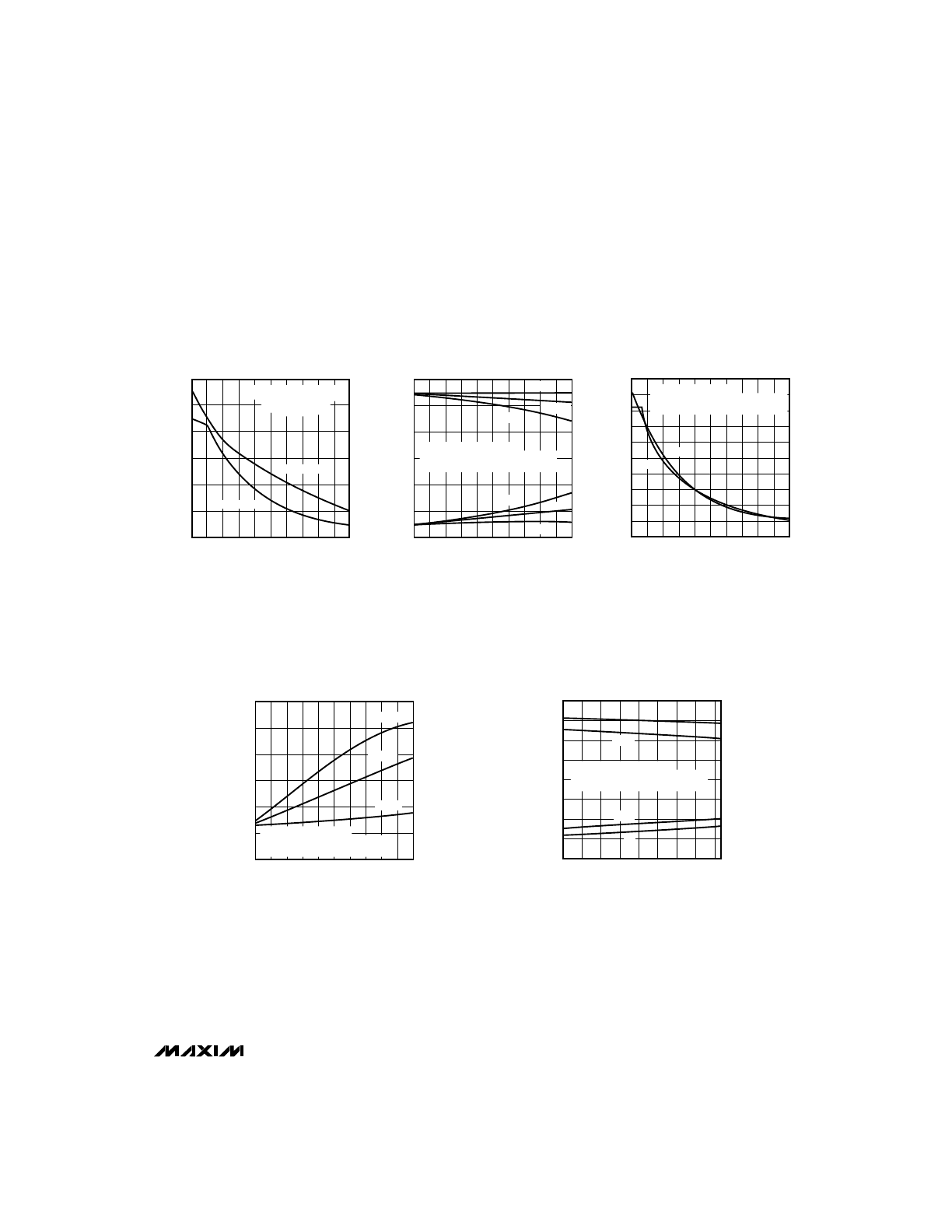
__________________________________________Typical Operating Characteristics
(Typical Operating Circuits, V
CC
= +5V, T
A
= +25°C, unless otherwise noted.)
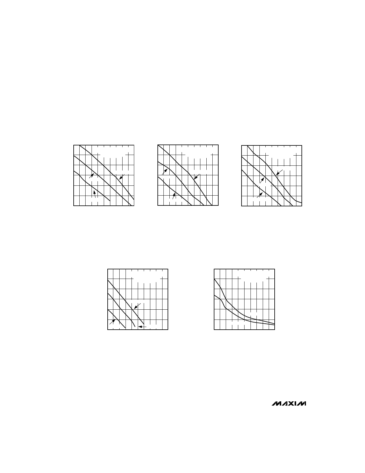
5.0
0
MAX232E
TRANSMITTER OUTPUT VOLTAGE
vs. LOAD CAPACITANCE
MAX202E-TOC1
LOAD CAPACITANCE (pF)
VOH, -VOL (V)
5.5
6.0
6.5
7.0
7.5
8.0
1000
2000
3000
4000
5000
V
CC
= 5.5V
ALL TRANSMITTERS LOADED
DATA RATE = 120kbps
R
L
= 3k
Ω
V
CC
= 4.5V
V
CC
= 5.0V
5.0
0
MAX202E/MAX203E
TRANSMITTER OUTPUT VOLTAGE
vs. LOAD CAPACITANCE
MAX202E-TOC2
LOAD CAPACITANCE (pF)
VOH, -VOL (V)
5.5
6.0
6.5
7.0
7.5
8.0
1000
2000
3000
4000
5000
V
CC
= 5.5V
V
CC
= 4.5V
V
CC
= 5.0V
ALL TRANSMITTERS LOADED
DATA RATE = 120kbps
R
L
= 3k
Ω
5.0
0
MAX241E
TRANSMITTER OUTPUT VOLTAGE
vs. LOAD CAPACITANCE
MAX202E-TOC3
LOAD CAPACITANCE (pF)
VOH, -VOL (V)
5.5
6.0
6.5
7.0
7.5
8.0
1000
2000
3000
4000
5000
V
CC
= 4.5V
V
CC
= 5.5V
V
CC
= 5.0V
ALL TRANSMITTERS LOADED
DATA RATE = 120kbps
R
L
= 3k
Ω
5.0
0
MAX211E/MAX213E
TRANSMITTER OUTPUT VOLTAGE
vs. LOAD CAPACITANCE
MAX202E-TOC4
LOAD CAPACITANCE (pF)
VOH, -VOL (V)
5.5
6.0
6.5
7.0
7.5
8.0
1000
2000
3000
4000
5000
V
CC
= 4.5V
V
CC
= 5.5V
V
CC
= 5.0V
ALL TRANSMITTERS LOADED
DATA RATE = 120kbps
R
L
= 3k
Ω
0
0
MAX211E/MAX213E/MAX241E
TRANSMITTER SLEW RATE
vs. LOAD CAPACITANCE
MAX202E-TOC5
LOAD CAPACITANCE (pF)
SLEW RATE ( V/
µ
s)
5
10
15
20
25
30
1000
2000
3000
4000
5000
+SLEW RATE
-SLEW RATE
ALL TRANSMITTERS LOADED
DATA RATE = 120kbps
R
L
= 3k
Ω
MAX202E–MAX213E, MAX232E/MAX241E
±15kV ESD-Protected, +5V RS-232 Transceivers
_______________________________________________________________________________________
5
____________________________Typical Operating Characteristics (continued)
(Typical Operating Circuits, V
CC
= +5V, T
A
= +25°C, unless otherwise noted.)
2
0
MAX202E/MAX203E/MAX232E
TRANSMITTER SLEW RATE
vs. LOAD CAPACITANCE
MAX202E-TOC6
LOAD CAPACITANCE (pF)
SLEW RATE ( V/
µ
s)
4
6
8
10
12
14
1000
2000
3000
4000
5000
+SLEW RATE
-SLEW RATE
ALL TRANSMITTERS LOADED
DATA RATE = 120kbps
R
L
= 3k
Ω
5.0
7.5
-7.5
0
3000
MAX205E–MAX208E
TRANSMITTER OUTPUT VOLTAGE
vs. LOAD CAPACITANCE
-5.0
2.5
MAX202E TOC-07
LOAD CAPACITANCE (pF)
OUTPUT VOLTAGE (V)
1000
2000
4000
5000
0
-2.5
V
CC
= +4.5V, R
L
= 3k
Ω
1 TRANSMITTER AT FULL DATA RATE
4 TRANSMITTERS AT 1/8 DATA RATE
240kbps
240kbps
120kbps
120kbps
20kbps
20kbps
45
50
20
0
3000
MAX205E–MAX208E
SUPPLY CURRENT
vs. LOAD CAPACITANCE
25
40
MAX202E TOC-09
LOAD CAPACITANCE (pF)
SUPPLY CURRENT (mA)
1000
2000
4000
5000
35
30
V
CC
= +4.5V, R
L
= 3k
Ω
1 TRANSMITTER AT FULL DATA RATE
4 TRANSMITTERS AT 1/8 DATA RATE
240kbps
120kbps
20kbps
10
12
0
0
3000
MAX205E–MAX208E
TRANSMITTER SLEW RATE
vs. LOAD CAPACITANCE
2
8
MAX202E TOC-08
LOAD CAPACITANCE (pF)
SLEW RATE (V/
µ
s)
1000
2000
4000
5000
6
4
20
18
16
14
V
CC
= +4.5V, R
L
= 3k
Ω
1 TRANSMITTER AT FULL DATA RATE
4 TRANSMITTERS AT 1/8 DATA RATE
FALL
RISE
2.5
5.0
-10.0
0
180
MAX205E–MAX208E
OUTPUT VOLTAGE vs. DATA RATE
-7.5
0
MAX202E TOC-10
DATA RATE (kbps)
OUTPUT VOLTAGE (V)
60
120
240
150
30
90
210
-2.5
-5.0
10.0
7.5
V
CC
= +4.5V, R
L
= 3k
Ω
1 TRANSMITTER AT FULL DATA RATE
4 TRANSMITTERS AT 1/8 DATA RATE
V+
V-
V
OUT
+
V
OUT-
MAX202E–MAX213E, MAX232E/MAX241E
±15kV ESD-Protected, +5V RS-232 Transceivers
6
_______________________________________________________________________________________
MAX203E
MAX205E
_____________________________________________________________Pin Descriptions
MAX202E/MAX232E
15
10, 11
9, 12
8, 13
Ground
19
RS-232 Driver Inputs
13, 14
7, 14
6
4, 5
RS-232 Receiver Outputs
12, 15
RS-232 Receiver Outputs
10, 17
RS-232 Driver Outputs
9, 18
-2V
CC
voltage generated by the charge pump
8
2
1, 3
Terminals for negative charge-pump capacitor
5, 7
+2V
CC
voltage generated by the charge pump
3
+4.5V to +5.5V Supply-Voltage Input
Terminals for positive charge-pump capacitor
2, 4
20
16
GND
T_IN
R_OUT
R_IN
T_OUT
V-
C2+, C2-
V+
C1+, C1-
V
CC
N.C.
No Connect—not internally connected.
1, 6, 11, 16
__
FUNCTION
NAME
PIN
DIP/SO
LCC
11, 15
12, 15
Connect pins together.
C2+
NAME
14
8
+2V
CC
voltage generated by the charge pump
V+
SO
C1-
T_IN
R_OUT
R_IN
T_OUT
GND
V
CC
C1+
C2-
V-
13
FUNCTION
14
1, 2
RS-232 Driver Inputs
Make no connection to this pin.
3, 20
RS-232 Receiver Outputs
4, 19
RS-232 Receiver Inputs
1, 2
3, 20
5, 18
RS-232 Transmitter Outputs
6, 9
Ground
7
+4.5V to +5.5V Supply-Voltage Input
13
Make no connection to this pin.
4,19
5,18
6, 9
11, 16
Connect pins together.
10, 17
-2V
CC
voltage generated by the charge pump. Connect pins together.
7
8
10, 16
12, 17
DIP
PIN
NAME
FUNCTION
T_OUT
RS-232 Driver Outputs
R_IN
RS-232 Receiver Inputs
R_OUT
TTL/CMOS Receiver Outputs. All receivers are inactive in shutdown.
PIN
1–4, 19
5, 10, 13, 18, 24
T_IN
TTL/CMOS Driver Inputs. Internal pull-ups to V
CC
.
GND
Ground
V
CC
+4.75V to +5.25V Supply Voltage
EN
Receiver Enable—active low
6, 9, 14, 17, 23
7, 8, 15, 16, 22
11
12
20
SHDN
Shutdown Control—active high
21
MAX202E–MAX213E, MAX232E/MAX241E
±15kV ESD-Protected, +5V RS-232 Transceivers
_______________________________________________________________________________________
7
MAX208E
________________________________________________Pin Descriptions (continued)
MAX206E
MAX207E
V+
NAME
FUNCTION
+2V
CC
generated by the charge pump
T_OUT
RS-232 Driver Outputs
11
R_IN
RS-232 Receiver Inputs
R_OUT
TTL/CMOS Receiver Outputs. All receivers are inactive in shutdown.
PIN
1, 2, 3, 24
4, 16, 23
T_IN
TTL/CMOS Driver Inputs. Internal pull-ups to V
CC
.
GND
Ground
V
CC
+4.5V to +5.5V Supply Voltage
C1+, C1-
Terminals for positive charge-pump capacitor
5, 17, 22
6, 7, 18, 19
8
9
10, 12
EN
Receiver Enable—active low
20
C2+, C2-
Terminals for negative charge-pump capacitor
V-
-2V
CC
generated by the charge pump
13, 14
15
SHDN
Shutdown Control—active high
21
V+
NAME
FUNCTION
+2V
CC
generated by the charge pump
T_OUT
RS-232 Driver Outputs
11
R_IN
RS-232 Receiver Inputs
R_OUT
TTL/CMOS Receiver Outputs. All receivers are inactive in shutdown.
PIN
1, 2, 3, 20, 24
4, 16, 23
T_IN
TTL/CMOS Driver Inputs. Internal pull-ups to V
CC
.
GND
Ground
C2+, C2-
V
CC
+4.75V to +5.25V Supply Voltage
Terminals for negative charge-pump capacitor
C1+, C1-
Terminals for positive charge-pump capacitor
5, 17, 22
6, 7, 18, 19, 21
8
V-
-2V
CC
generated by the charge pump
13, 14
15
9
10, 12
V+
NAME
FUNCTION
+2V
CC
generated by the charge pump
T_OUT
RS-232 Driver Outputs
11
R_IN
RS-232 Receiver Inputs
R_OUT
TTL/CMOS Receiver Outputs. All receivers are inactive in shutdown.
PIN
1, 2, 20, 24
3, 7, 16, 23
T_IN
TTL/CMOS Driver Inputs. Internal pull-ups to V
CC
.
GND
Ground
C2+, C2-
V
CC
+4.5V to +5.5V Supply Voltage
Terminals for negative charge-pump capacitor
C1+, C1-
Terminals for positive charge-pump capacitor
4, 6, 17, 22
5, 18, 19, 21
8
V-
-2V
CC
generated by the charge pump
13, 14
15
9
10, 12
MAX202E–MAX213E, MAX232E/MAX241E
±15kV ESD-Protected, +5V RS-232 Transceivers
8
_______________________________________________________________________________________
V+
GND
MAX206E
MAX211E
MAX213E
MAX241E
0.1µF
*
V
CC
0.1µF
*
R1 TO R5
T1 TO T5
0.1µF
*
C1+
C1-
C2+
C2-
V
CC
+5.5V
T_OUT
R_OUT
400k
5k
I
SHDN
0V OR +5.5V
DRIVE
0.1µF
*
0.1µF
*
3k
+5.5V
R_IN
T_IN
CAPACITORS MAY BE
POLARIZED OR UNPOLARIZED
( ) ARE FOR MAX213E
*
1µF FOR MAX241E
EN (EN)
SHDN (SHDN)
+5.5V (0V)
V-
+5.5V
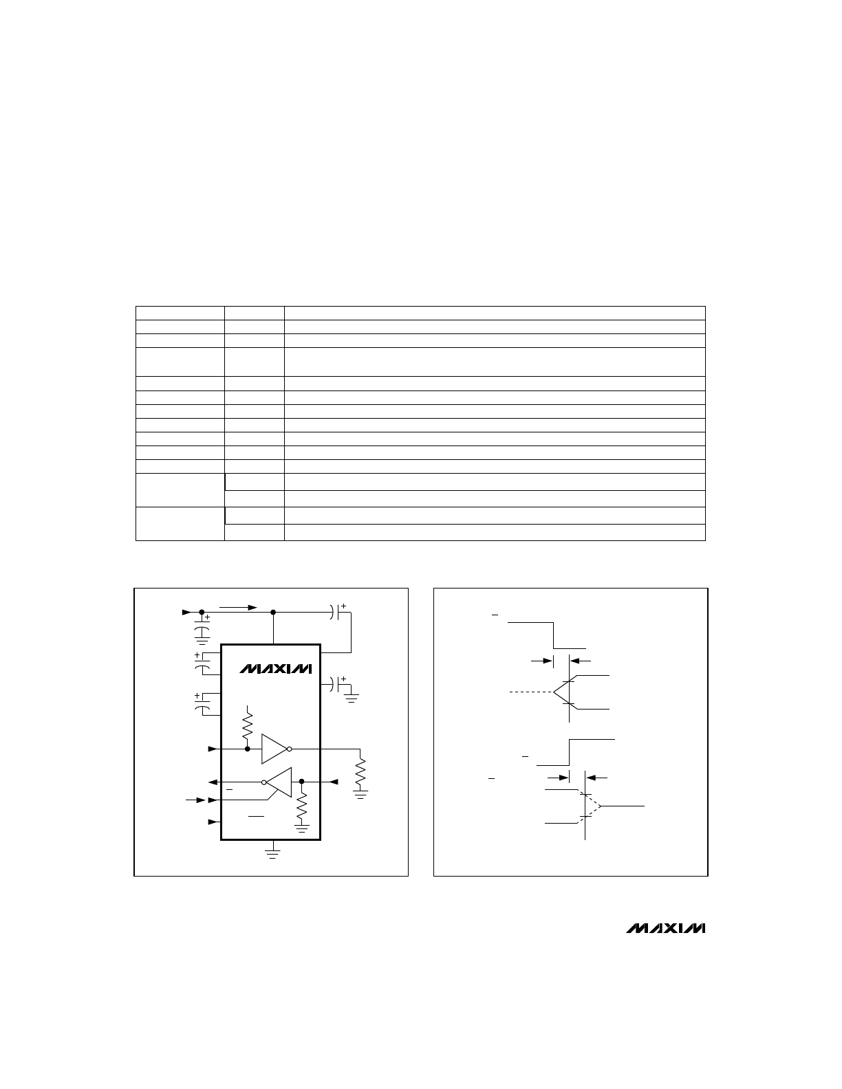
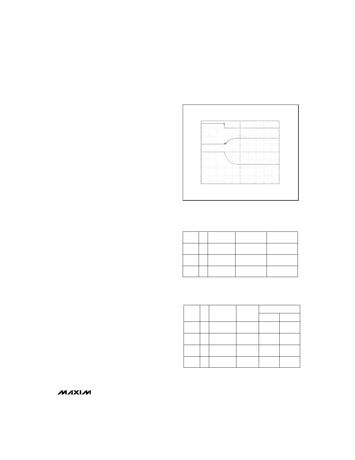
Figure 1. Shutdown-Current Test Circuit (MAX206E,
MAX211E/MAX213E/MAX241E)
+3.5V
EN
INPUT
OUTPUT ENABLE TIME
+2.5V
RECEIVER
OUTPUT
C
L
= 150pF
RECEIVER
OUTPUTS
OUTPUT DISABLE TIME
V
OH
- 0.1V
V
OH
V
OL
V
OL
+ 0.1V
R
L
= 1k
Ω
NOTE:
POLARITY OF EN
IS REVERSED
FOR THE
MAX213E
+0.8V
0V
+3V
+3V
EN
INPUT
0V
Figure 2. Receiver Output Enable and Disable Timing
(MAX205E/MAX206E/MAX211E/MAX213E/MAX241E)
17
NAME
FUNCTION
V-
T_OUT
RS-232 Driver Outputs
-2V
CC
voltage generated by the charge pump
R_IN
RS-232 Receiver Inputs
24
R_OUT
TTL/CMOS Receiver Outputs. For the MAX213E, receivers R4 and R5 are active in shutdown
mode when EN = 1. For the MAX211E and MAX241E, all receivers are inactive in shutdown.
PIN
1, 2, 3, 28
4, 9, 18, 23, 27
EN
T_IN
TTL/CMOS Driver Inputs. Only the MAX211E, MAX213E, and MAX241E have internal pull-ups to V
CC.
Receiver Enable—active high (MAX213E)
GND
Ground
25
V
CC
+4.5V to +5.5V Supply Voltage
SHDN
C1+, C1-
Terminals for positive charge-pump capacitor
5, 8, 19, 22, 26
6, 7, 20, 21
10
Shutdown Control—active low (MAX213E)
V+
+2V
CC
voltage generated by the charge pump
C2+, C2-
Terminals for negative charge-pump capacitor
11
12, 14
13
15, 16
EN
Receiver Enable—active low (MAX211E, MAX241E)
SHDN
Shutdown Control—active high (MAX211E, MAX241E)
________________________________________________Pin Descriptions (continued)
MAX211E/MAX213E/MAX241E
MAX202E–MAX213E, MAX232E/MAX241E
±15kV ESD-Protected, +5V RS-232 Transceivers
_______________________________________________________________________________________
9
V+
MAX2_ _E
0.1µF
*
V
CC
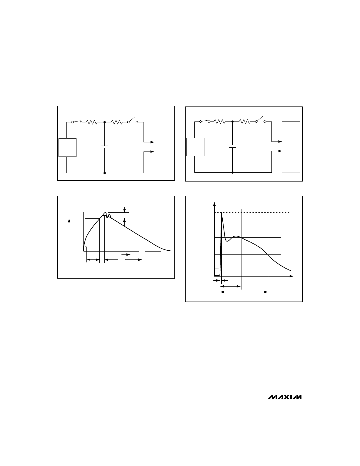
0.1µF
*
T_
R_
0.1µF
*
C1+
C1-
C2+
C2-
V
CC
T_OUT
R_OUT
EN (EN)
SHDN (SHDN)
400k
5k
0.1µF
*
0.1µF
*
3k
+5V
R_IN
T_IN
MINIMUM SLEW-RATE TEST CIRCUIT
0V (+5V)
0V (+5V)
2500pF
V-
V+
0.1µF
*
V
CC
0.1µF
*
R_
T_
0.1µF
*
C1+
C1-
C2+
C2-
V
CC
T_OUT
R_OUT
EN (EN)
SHDN (SHDN)
400k
5k
0.1µF
*
0.1µF
*
7k
+5V
R_IN
T_IN
MAXIMUM SLEW-RATE TEST CIRCUIT
0V (+5V)
0V (+5V)
50pF
V-
( ) ARE FOR MAX213E
* 1
µ
F FOR MAX232E/MAX241E
MAX2_ _E
TRANSMITTER INPUT PULL-UP RESISTORS, ENABLE, AND SHUTDOWN ARE NOT PROVIDED ON THE MAX202E, MAX203E, AND MAX232E.
ENABLE AND SHUTDOWN ARE NOT PROVIDED ON THE MAX207E AND MAX208E.
Figure 3. Transition Slew-Rate Circuit
_______________Detailed Description
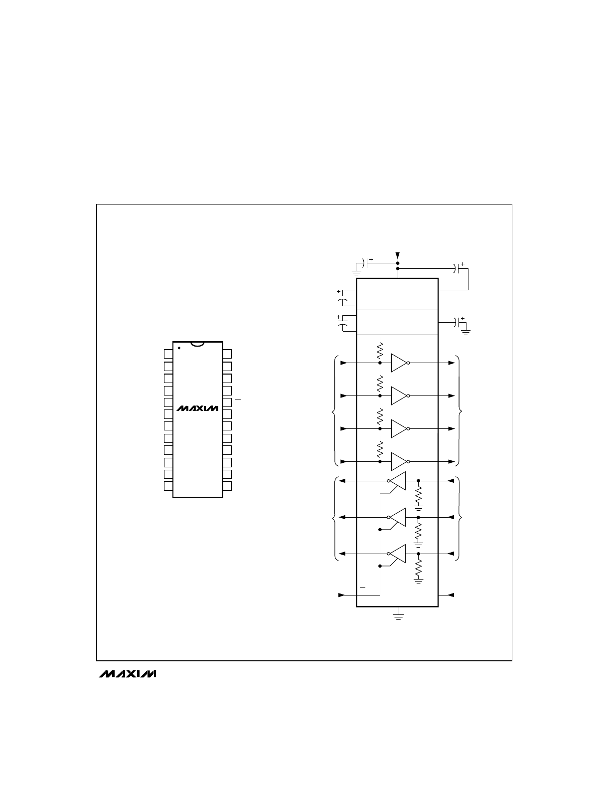
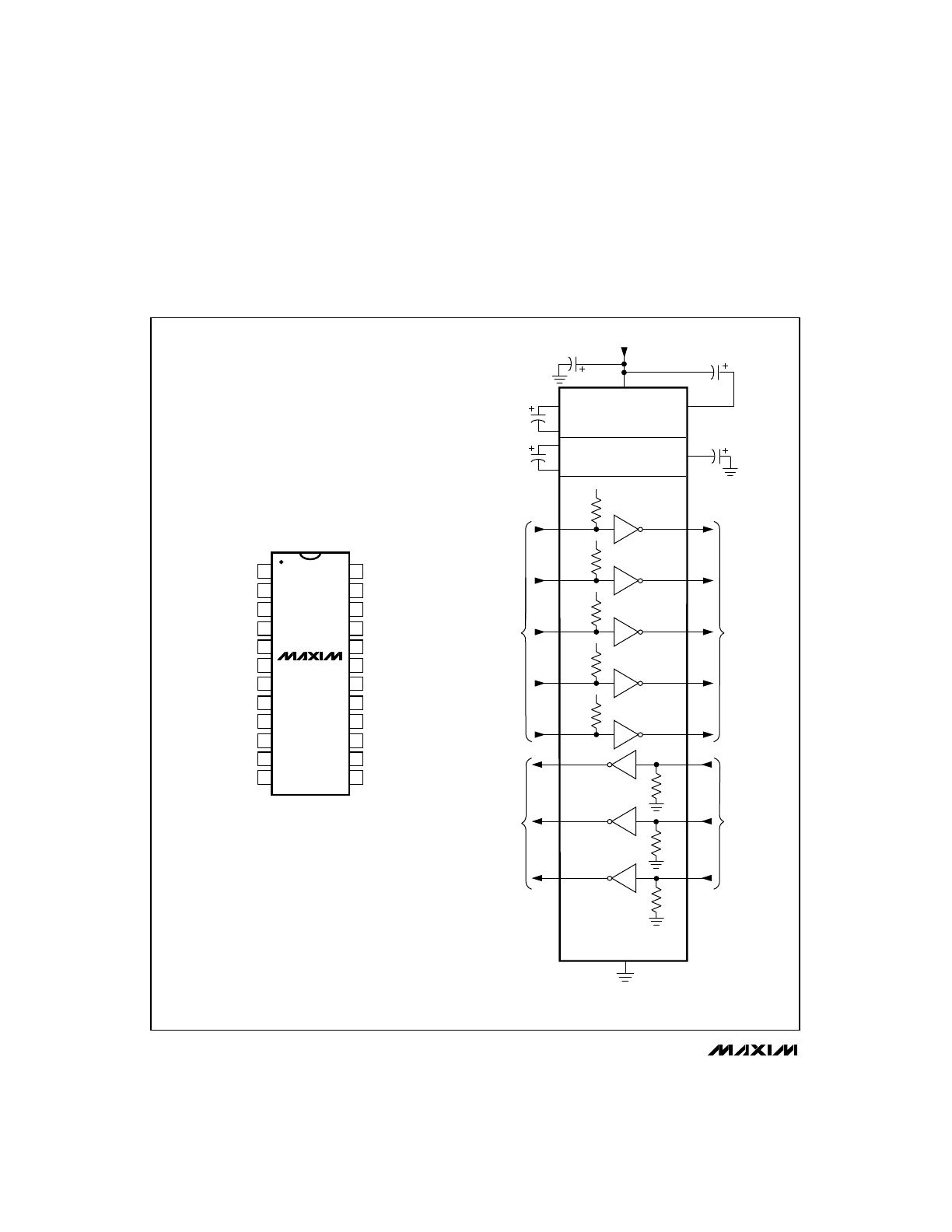
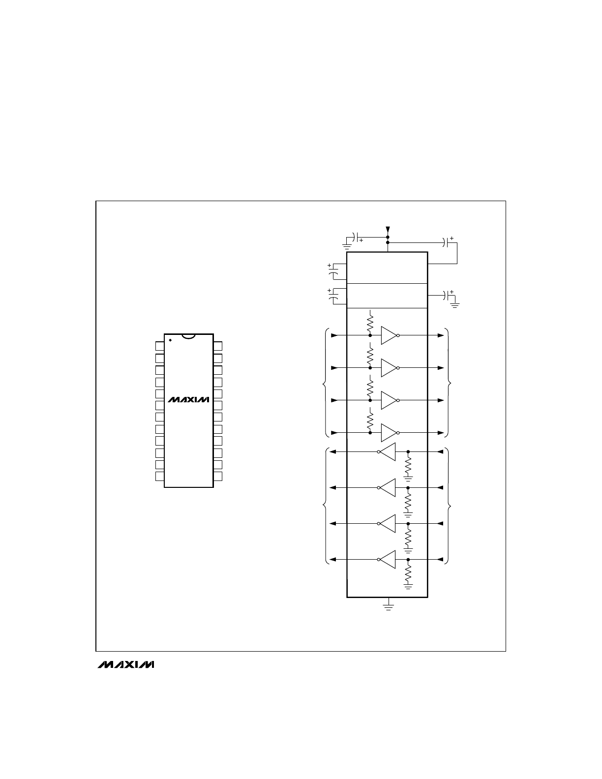
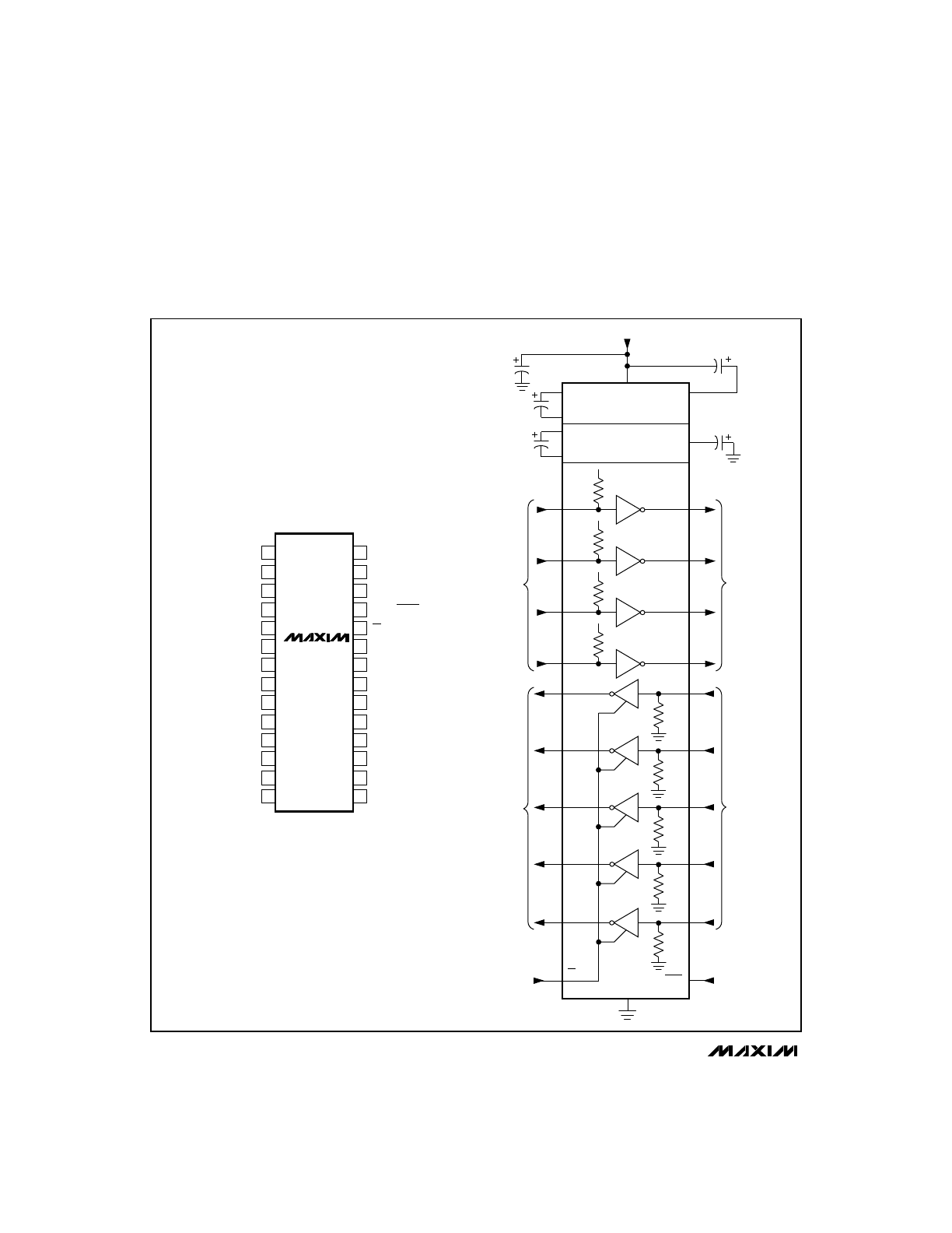
The MAX202E–MAX213E, MAX232E/MAX241E consist of
three sections: charge-pump voltage converters,
drivers (transmitters), and receivers. These E versions
provide extra protection against ESD. They survive
±15kV discharges to the RS-232 inputs and outputs,
tested using the Human Body Model. When tested
according to IEC1000-4-2, they survive ±8kV contact-
discharges and ±15kV air-gap discharges. The rugged
E versions are intended for use in harsh environments
or applications where the RS-232 connection is
frequently changed (such as notebook computers). The
standard (non-“E”) MAX202, MAX203, MAX205–
MAX208, MAX211, MAX213, MAX232, and MAX241 are
recommended for applications where cost is critical.
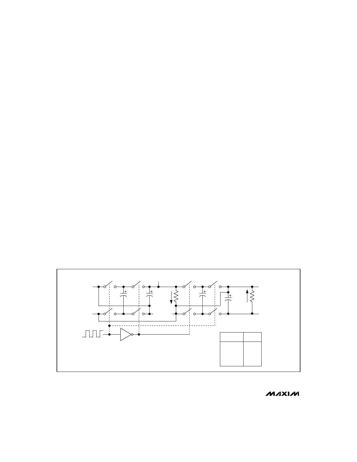
+5V to ±10V Dual Charge-Pump
Voltage Converter
The +5V to ±10V conversion is performed by dual
charge-pump voltage converters (Figure 4). The first
charge-pump converter uses capacitor C1 to double
the +5V into +10V, storing the +10V on the output filter
capacitor, C3. The second uses C2 to invert the +10V
into -10V, storing the -10V on the V- output filter
capacitor, C4.
In shutdown mode, V+ is internally connected to V
CC
by
a 1k
Ω
pull-down resistor, and V- is internally connected
to ground by a 1k
Ω
pull-up resistor.
RS-232 Drivers
With V
CC
= 5V, the typical driver output voltage swing
is ±8V when loaded with a nominal 5k
Ω
RS-232
receiver. The output swing is guaranteed to meet
EIA/TIA-232E and V.28 specifications that call for ±5V
minimum output levels under worst-case conditions.
These include a 3k
Ω
load, minimum V
CC
, and
maximum operating temperature. The open-circuit
output voltage swings from (V+ - 0.6V) to V-.
Input thresholds are CMOS/TTL compatible. The
unused drivers’ inputs on the MAX205E–MAX208E,
MAX211E, MAX213E, and MAX241E can be left
unconnected because 400k
Ω
pull-up resistors to V
CC
are included on-chip. Since all drivers invert, the pull-
up resistors force the unused drivers’ outputs low. The
MAX202E, MAX203E, and MAX232E do not have pull-
up resistors on the transmitter inputs.
MAX202E–MAX213E, MAX232E/MAX241E
±15kV ESD-Protected, +5V RS-232 Transceivers
10
______________________________________________________________________________________
When in low-power shutdown mode, the MAX205E/
MAX206E/MAX211E/MAX213E/MAX241E driver outputs
are turned off and draw only leakage currents—even if
they are back-driven with voltages between 0V and
12V. Below -0.5V in shutdown, the transmitter output is
diode-clamped to ground with a 1k
Ω
series
impedance.
RS-232 Receivers
The receivers convert the RS-232 signals to CMOS-logic
output levels. The guaranteed 0.8V and 2.4V receiver
input thresholds are significantly tighter than the ±3V
thresholds required by the EIA/TIA-232E specification.
This allows the receiver inputs to respond to TTL/CMOS-
logic levels, as well as RS-232 levels.
The guaranteed 0.8V input low threshold ensures that
receivers shorted to ground have a logic 1 output. The
5k
Ω
input resistance to ground ensures that a receiver
with its input left open will also have a logic 1 output.
Receiver inputs have approximately 0.5V hysteresis.
This provides clean output transitions, even with slow
rise/fall-time signals with moderate amounts of noise
and ringing.
In shutdown, the MAX213E’s R4 and R5 receivers have
no hysteresis.
Shutdown and Enable Control
(MAX205E/MAX206E/MAX211E/
MAX213E/MAX241E)
In shutdown mode, the charge pumps are turned off,
V+ is pulled down to V
CC
, V- is pulled to ground, and
the transmitter outputs are disabled. This reduces
supply current typically to 1µA (15µA for the MAX213E).
The time required to exit shutdown is under 1ms, as
shown in Figure 5.
Receivers
All MAX213E receivers, except R4 and R5, are put into
a high-impedance state in shutdown mode (see Tables
1a and 1b). The MAX213E’s R4 and R5 receivers still
function in shutdown mode. These two awake-in-
shutdown receivers can monitor external activity while
maintaining minimal power consumption.
The enable control is used to put the receiver outputs into
a high-impedance state, to allow wire-OR connection of
two EIA/TIA-232E ports (or ports of different types) at the
UART. It has no effect on the RS-232 drivers or the
charge pumps.
Note: The enable control pin is active low for the
MAX211E/MAX241E (
EN
), but is active high for the
MAX213E (EN). The shutdown control pin is active high
for the MAX205E/MAX206E/MAX211E/MAX241E
(SHDN), but is active low for the MAX213E (
SHDN
).
C1-
I
L
-
R
L
-
V+
S1
V -
f
CLK
S2
S5
S6
C1
C3
C2
I
L
+
R
L
+
S3
S4
S7
S8
C4
C1+
GND
GND
V
CC
V
CC
C2-
C2+
PART
f
CLK
(kHz)
MAX202E
MAX211E/213E
MAX232E
MAX203E
230
MAX205E–208E
200
200
140
MAX241E
30
230
Figure 4. Charge-Pump Diagram
MAX202E–MAX213E, MAX232E/MAX241E
±15kV ESD-Protected, +5V RS-232 Transceivers
______________________________________________________________________________________
11
V+
V-
200
µ
s/div
3V
0V
10V
5V
0V
-5V
-10V
SHDN
MAX211E
Figure 5. MAX211E V+ and V- when Exiting Shutdown (0.1µF
capacitors)
X = Don't Care
*Active = active with reduced performance
SHDN
EN
OPERATION
STATUS
Tx
Rx
0
0
Normal
Operation
All Active
All Active
0
1
Normal
Operation
All Active
All High-Z
1
X
Shutdown
All High-Z
All High-Z
Table 1a. MAX205E/MAX206E/MAX211E/
MAX241E Control Pin Configurations
Table 1b. MAX213E Control Pin
Configurations
The MAX213E’s receiver propagation delay is typically
0.5µs in normal operation. In shutdown mode,
propagation delay increases to 4µs for both rising and
falling transitions. The MAX213E’s receiver inputs have
approximately 0.5V hysteresis, except in shutdown,
when receivers R4 and R5 have no hysteresis.
When entering shutdown with receivers active, R4 and
R5 are not valid until 80µs after
SHDN is driven low.
When coming out of shutdown, all receiver outputs are
invalid until the charge pumps reach nominal voltage
levels (less than 2ms when using 0.1µF capacitors).
±15kV ESD Protection
As with all Maxim devices, ESD-protection structures
are incorporated on all pins to protect against
electrostatic discharges encountered during handling
and assembly. The driver outputs and receiver inputs
have extra protection against static electricity. Maxim’s
engineers developed state-of-the-art structures to
protect these pins against ESD of ±15kV without
damage. The ESD structures withstand high ESD in all
states: normal operation, shutdown, and powered
down. After an ESD event, Maxim’s E versions keep
working without latchup, whereas competing RS-232
products can latch and must be powered down to
remove latchup.
ESD protection can be tested in various ways; the
transmitter outputs and receiver inputs of this product
family are characterized for protection to the following
limits:
1) ±15kV using the Human Body Model
2) ±8kV using the contact-discharge method specified
in IEC1000-4-2
3) ±15kV using IEC1000-4-2’s air-gap method.
ESD Test Conditions
ESD performance depends on a variety of conditions.
Contact Maxim for a reliability report that documents
test set-up, test methodology, and test results.
Human Body Model
Figure 6a shows the Human Body Model, and Figure
6b shows the current waveform it generates when
discharged into a low impedance. This model consists
of a 100pF capacitor charged to the ESD voltage of
interest, which is then discharged into the test device
through a 1.5k
Ω
resistor.
SHDN
EN
OPERATION
STATUS
Tx 1–4
0
0
Shutdown
All High-Z
0
1
Shutdown
All High-Z
1
0
Normal
Operation
1
1
Normal
Operation
All Active
All Active
Active
1–3
4, 5
High-Z
Active
High-Z
High-Z
High-Z
Active*
High-Z
Rx
MAX202E–MAX213E, MAX232E/MAX241E
±15kV ESD-Protected, +5V RS-232 Transceivers
12
______________________________________________________________________________________
IEC1000-4-2
The IEC1000-4-2 standard covers ESD testing and
performance of finished equipment; it does not
specifically refer to integrated circuits. The
MAX202E/MAX203E–MAX213E, MAX232E/MAX241E
help you design equipment that meets level 4 (the
highest level) of IEC1000-4-2, without the need for
additional ESD-protection components.
The major difference between tests done using the
Human Body Model and IEC1000-4-2 is higher peak
current in IEC1000-4-2, because series resistance is
lower in the IEC1000-4-2 model. Hence, the ESD
withstand voltage measured to IEC1000-4-2 is
generally lower than that measured using the Human
Body Model. Figure 7b shows the current waveform for
the 8kV IEC1000-4-2 level-four ESD contact-discharge
test.
The air-gap test involves approaching the device with a
charged probe. The contact-discharge method
connects the probe to the device before the probe is
energized.
Machine Model
The Machine Model for ESD tests all pins using a
200pF storage capacitor and zero discharge
resistance. Its objective is to emulate the stress caused
by contact that occurs with handling and assembly
during manufacturing. Of course, all pins require this
protection during manufacturing, not just RS-232 inputs
and outputs. Therefore, after PC board assembly, the
Machine Model is less relevant to I/O ports.
CHARGE CURRENT
LIMIT RESISTOR
DISCHARGE
RESISTANCE
STORAGE
CAPACITOR
Cs
150pF
R
C
50M to 100M
R
D
330
Ω
HIGH-
VOLTAGE
DC
SOURCE
DEVICE
UNDER
TEST
Figure 7a. IEC1000-4-2 ESD Test Model
tr = 0.7ns to 1ns
30ns
60ns
t
100%
90%
10%
I
PEAK
I
Figure 7b. IEC1000-4-2 ESD Generator Current Waveform
CHARGE-CURRENT
LIMIT RESISTOR
DISCHARGE
RESISTANCE
STORAGE
CAPACITOR
Cs
100pF
R
C
1M
R
D
1500
Ω
HIGH-
VOLTAGE
DC
SOURCE
DEVICE
UNDER
TEST
Figure 6a. Human Body ESD Test Model
I
P
100%
90%
36.8%
t
RL
TIME
t
DL
CURRENT WAVEFORM
PEAK-TO-PEAK RINGING
(NOT DRAWN TO SCALE)
Ir
10%
0
0
AMPERES
Figure 6b. Human Body Model Current Waveform
MAX202E–MAX213E, MAX232E/MAX241E
±15kV ESD-Protected, +5V RS-232 Transceivers
______________________________________________________________________________________
13
__________Applications Information
Capacitor Selection
The capacitor type used for C1–C4 is not critical for
proper operation. The MAX202E, MAX206–MAX208E,
MAX211E, and MAX213E require 0.1µF capacitors,
and the MAX232E and MAX241E require 1µF
capacitors, although in all cases capacitors up to 10µF
can be used without harm. Ceramic, aluminum-
electrolytic, or tantalum capacitors are suggested for
the 1µF capacitors, and ceramic dielectrics are
suggested for the 0.1µF capacitors. When using the
minimum recommended capacitor values, make sure
the capacitance value does not degrade excessively
as the operating temperature varies. If in doubt, use
capacitors with a larger (e.g., 2x) nominal value. The
capacitors’ effective series resistance (ESR), which
usually rises at low temperatures, influences the
amount of ripple on V+ and V-.
Use larger capacitors (up to 10µF) to reduce the output
impedance at V+ and V-. This can be useful when
“stealing” power from V+ or from V-. The MAX203E and
MAX205E have internal charge-pump capacitors.
Bypass V
CC
to ground with at least 0.1µF. In
applications sensitive to power-supply noise generated
by the charge pumps, decouple V
CC
to ground with a
capacitor the same size as (or larger than) the charge-
pump capacitors (C1–C4).
V+ and V- as Power Supplies
A small amount of power can be drawn from V+ and V-,
although this will reduce both driver output swing and
noise margins. Increasing the value of the charge-pump
capacitors (up to 10µF) helps maintain performance
when power is drawn from V+ or V-.
Driving Multiple Receivers
Each transmitter is designed to drive a single receiver.
Transmitters can be paralleled to drive multiple
receivers.
Driver Outputs when Exiting Shutdown
The driver outputs display no ringing or undesirable
transients as they come out of shutdown.
High Data Rates
These transceivers maintain the RS-232 ±5.0V
minimum driver output voltages at data rates of over
120kbps. For data rates above 120kbps, refer to the
Transmitter Output Voltage vs. Load Capacitance
graphs in the
Typical Operating Characteristics.
Communication at these high rates is easier if the
capacitive loads on the transmitters are small; i.e.,
short cables are best.
Table 2. Summary of EIA/TIA-232E, V.28 Specifications
PARAMETER
CONDITIONS
EIA/TIA-232E, V.28
SPECIFICATIONS
0 Level
3k
Ω
to 7k
Ω
load
+5V to +15V
Data Rate
3k
Ω ≤
R
L
≤
7k
Ω
, C
L
≤
2500pF
Up to 20kbps
+3V to +15V
Instantaneous Slew Rate, Max
3k
Ω ≤
R
L
≤
7k
Ω
, C
L
≤
2500pF
30V/µs
Driver Output Short-Circuit Current, Max
100mA
Transition Rate on Driver Output
V.28
1ms or 3% of the period
Driver Output Resistance
-2V < V
OUT
< +2V
300
Ω
EIA/TIA-232E
4% of the period
Driver Output Level, Max
No load
±25V
Driver Output Voltage
3k
Ω
to 7k
Ω
load
-5V to -15V
0 Level
1 Level
1 Level
Receiver Input Level
±25V
Receiver Input Voltage
-3V to -15V
MAX202E–MAX213E, MAX232E/MAX241E
±15kV ESD-Protected, +5V RS-232 Transceivers
14
______________________________________________________________________________________
____________Pin Configurations and Typical Operating Circuits (continued)
TOP VIEW
1
4
5
TTL/CMOS
INPUTS
TTL/CMOS
OUTPUTS
11
10
12
9
3
GND
C1-
C2+
5k
5k
C2-
T1IN
T2IN
R2OUT
R1OUT
V
CC
+5V TO +10V
VOLTAGE DOUBLER
+10V TO -10V
VOLTAGE INVERTER
16
2
6
14
7
13
8
0.1
µ
F
0.1
µ
F*
16V
0.1
µ
F*
6.3V
0.1
µ
F*
16V
0.1
µ
F*
6.3V
C1+
RS-232
OUTPUTS
RS-232
INPUTS
-10V
+10V
V+
+5V INPUT
V-
T1OUT
R1IN
R2IN
T2OUT
T1
15
T2
R1
R2
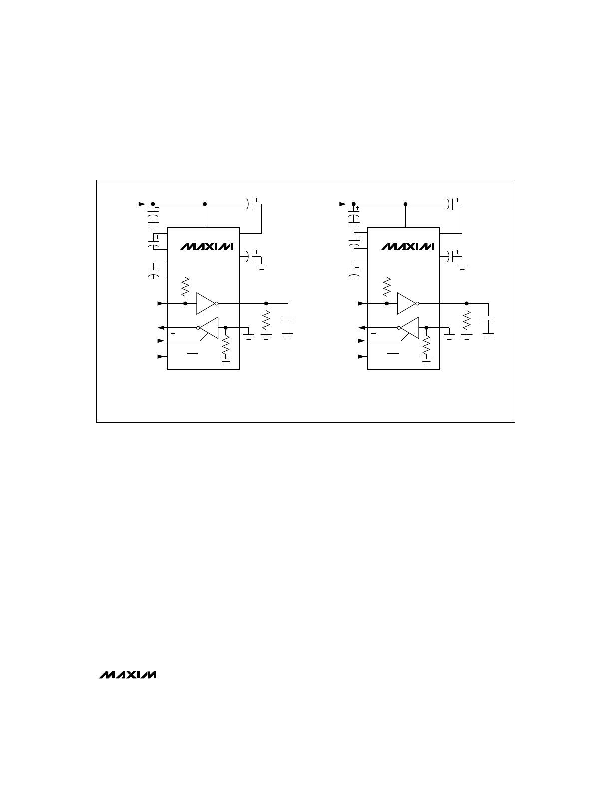
PIN NUMBERS ON TYPICAL OPERATING CIRCUIT REFER TO DIP/SO PACKAGE, NOT LCC.
* 1.0
µ
F CAPACITORS, MAX232E ONLY.
16
15
14
13
12
11
10
9
1
2
3
4
5
6
7
8
V
CC
GND
T1OUT
R1IN
C2+
C1-
V+
C1+
MAX202E
MAX232E
R1OUT
T1IN
T2IN
R2OUT
R2IN
T2OUT
V-
C2-
DIP/SO
Table 3. DB9 Cable Connections
Commonly Used for EIA/TIAE-232E and
V.24 Asynchronous Interfaces
PIN
CONNECTION
2
Receive Data (RD)
Data from DCE
3
Transmit Data (TD)
Data from DTE
4
Data Terminal Ready
Handshake from DTE
5
Signal Ground
Reference point for
signals
6
Data Set Ready (DSR)
Handshake from DCE
7
Request to Send (RTS)
Handshake from DTE
8
Clear to Send (CTS)
Handshake from DCE
9
Ring Indicator
Handshake from DCE
1
Received Line Signal
Detector (sometimes
called Carrier Detect,
DCD)
Handshake from DCE
MAX202E–MAX213E, MAX232E/MAX241E
±15kV ESD-Protected, +5V RS-232 Transceivers
______________________________________________________________________________________
15
____________Pin Configurations and Typical Operating Circuits (continued)
20
19
18
17
16
15
14
13
1
2
3
4
5
6
7
8
R2OUT
R2IN
T2OUT
V-
R1IN
R1OUT
T1IN
T2IN
C2-
C2+
V+ (C1-)
C1- (C1+)
C1+ (V+)
V
CC
GND
T1OUT
12
11
9
10
V- (C2+)
C2+ (C2-)
C2- (V-)
GND
DIP/SO
MAX203E
TOP VIEW
TTL/CMOS
INPUTS
TTL/CMOS
OUTPUTS
2
1
3
20
GND
GND
400k
5k
5k
T1IN
T2IN
R2OUT
R1OUT
V
CC
7
5
18
4
19
0.1
µ
F
RS-232
OUTPUTS
RS-232
INPUTS
+5V
400k
+5V
+5V INPUT
T1OUT
R1IN
R2IN
T2OUT
T1
9
6
T2
R1
R2
V-
V-
C1-
C1+
8(13)
13(14)
12(10)
17
14(8)
DO NOT MAKE
CONNECTION TO
THESE PINS
INTERNAL -10V
POWER SUPPLY
INTERNAL +10V
POWER SUPPLY
V+
C2-
C2-
C2+
C2+
11
15
16
10 (11)
PIN NUMBERS IN ( ) ARE FOR SO PACKAGE.
(12)
MAX202E–MAX213E, MAX232E/MAX241E
±15kV ESD-Protected, +5V RS-232 Transceivers
16
______________________________________________________________________________________
____________Pin Configurations and Typical Operating Circuits (continued)
T4OUT
T3OUT
T1OUT
T2OUT
R2IN
R2OUT
T2IN
T1IN
R1OUT
R1IN
GND
V
CC
DIP
TOP VIEW
MAX205E
1
2
3
4
5
6
7
8
9
10
11
12
24
23
22
21
20
19
18
17
16
15
14
13
R3IN
R3OUT
T5IN
SHDN
EN
T5OUT
R4IN
R4OUT
T4IN
T3IN
R5OUT
R5IN
V
CC
TTL/CMOS
INPUTS
GND
SHDN
+5V INPUT
+5V
T2OUT
400k
T2IN
T2
4
+5V
T3OUT
400k
T3IN
T3
2
+5V
T4OUT
400k
T4IN
T4
1
+5V
T5OUT
400k
T5IN
T5
19
5k
R1
R1OUT
R1IN
5k
R2
R2OUT
R2IN
5k
R3
R3OUT
R3IN
8
7
15
16
22
9
6
23
10
5
24
5k
R4OUT
R4IN
17
18
5k
R5
R5OUT
R5IN
14
13
EN
20
21
11
12
TTL/CMOS
OUTPUTS
+5V
T1OUT
400k
T1IN
T1
3
RS-232
OUTPUTS
RS-232
INPUTS
R4
0.1µF
MAX202E–MAX213E, MAX232E/MAX241E
±15kV ESD-Protected, +5V RS-232 Transceivers
______________________________________________________________________________________
17
____________Pin Configurations and Typical Operating Circuits (continued)
T3OUT
T1OUT
T2OUT
R1IN
R1OUT
T2IN
T1IN
GND
V
CC
C1+
V+
C1-
DIP/SO/SSOP
TOP VIEW
MAX206E
1
2
3
4
5
6
7
8
9
10
11
12
24
23
22
21
20
19
18
17
16
15
14
13
T4OUT
R2IN
R2OUT
SHDN
EN
T4IN
T3IN
R3OUT
R3IN
V-
C2-
C2+
V
CC
TTL/CMOS
INPUTS
GND
SHDN
+5V INPUT
+5V
T1OUT
400k
T1IN
T1
2
+5V
T2OUT
400k
T2IN
T2
3
+5V
T3OUT
400k
T3IN
T3
1
+5V
T4OUT
400k
T4IN
T4
24
5k
R1
R1OUT
R1IN
5k
R2
R2OUT
R2IN
5k
R3
R3OUT
R3IN
7
6
18
19
5
22
17
4
23
16
EN
20
21
8
9
TTL/CMOS
OUTPUTS
RS-232
OUTPUTS
RS-232
INPUTS
0.1µF
V+
0.1µF
6.3V
0.1µF
16V
C1+
C1-
0.1µF
6.3V
0.1µF
16V
V-
10
12
13
14
C2+
C2-
11
15
+5V TO +10V
VOLTAGE DOUBLER
+10V TO -10V
VOLTAGE INVERTER
MAX202E–MAX213E, MAX232E/MAX241E
±15kV ESD-Protected, +5V RS-232 Transceivers
18
______________________________________________________________________________________
____________Pin Configurations and Typical Operating Circuits (continued)
T3OUT
T1OUT
T2OUT
R1IN
R1OUT
T2IN
T1IN
GND
V
CC
C1+
V+
C1-
DIP/SO/SSOP
TOP VIEW
MAX207E
1
2
3
4
5
6
7
8
9
10
11
12
24
23
22
21
20
19
18
17
16
15
14
13
T4OUT
R2IN
R2OUT
T5IN
T5OUT
T4IN
T3IN
R3OUT
R3IN
V-
C2-
C2+
V
CC
TTL/CMOS
INPUTS
GND
+5V INPUT
+5V
T2OUT
400k
T2IN
T2
+5V
T1OUT
400k
T1IN
T1
3
+5V
T3OUT
400k
T3IN
T3
1
+5V
T4OUT
400k
T4IN
T4
24
+5V
T5OUT
400k
T5IN
T5
20
5k
R1
R1OUT
R1IN
5k
R2
R2OUT
R2IN
5k
R3
R3OUT
R3IN
7
6
18
19
21
5
22
17
4
23
16
8
9
TTL/CMOS
OUTPUTS
RS-232
OUTPUTS
RS-232
INPUTS
0.1µF
V+
0.1µF
6.3V
0.1µF
16V
C1+
C1-
0.1µF
6.3V
0.1µF
16V
V-
10
12
13
14
C2+
C2-
11
15
+5V TO +10V
VOLTAGE DOUBLER
+10V TO -10V
VOLTAGE INVERTER
2
MAX202E–MAX213E, MAX232E/MAX241E
±15kV ESD-Protected, +5V RS-232 Transceivers
______________________________________________________________________________________
19
____________Pin Configurations and Typical Operating Circuits (continued)
T2OUT
T1OUT
R2IN
R2OUT
T1IN
R1OUT
R1IN
GND
V
CC
C1+
V+
C1-
DIP/SO/SSOP
TOP VIEW
MAX208E
1
2
3
4
5
6
7
8
9
10
11
12
24
23
22
21
20
19
18
17
16
15
14
13
T3OUT
R3IN
R3OUT
T4IN
T4OUT
T3IN
T2IN
R4OUT
R4IN
V-
C2-
C2+
V
CC
TTL/CMOS
INPUTS
GND
+5V INPUT
+5V
T1OUT
400k
T1IN
T1
2
+5V
T2OUT
400k
T2IN
T2
1
+5V
T3OUT
400k
T3IN
T3
24
+5V
T4OUT
400k
T4IN
T4
20
5k
R1
R1OUT
R1IN
5k
R2
R2OUT
R2IN
5k
5k
R3
R3OUT
R3IN
5
18
19
21
6
4
22
7
3
23
8
9
TTL/CMOS
OUTPUTS
RS-232
OUTPUTS
RS-232
INPUTS
R4
R4OUT
R4IN
17
16
0.1µF
V+
0.1µF
6.3V
0.1µF
16V
C1+
C1-
0.1µF
6.3V
0.1µF
16V
V-
10
12
13
14
C2+
C2-
11
15
+5V TO +10V
VOLTAGE DOUBLER
+10V TO -10V
VOLTAGE INVERTER
MAX202E–MAX213E, MAX232E/MAX241E
±15kV ESD-Protected, +5V RS-232 Transceivers
20
______________________________________________________________________________________
____________Pin Configurations and Typical Operating Circuits (continued)
T3OUT
T1OUT
T2OUT
R2IN
R2OUT
T2IN
T1IN
R1OUT
R1IN
GND
V
CC
C1+
V+
C1-
SO/SSOP
TOP VIEW
MAX211E
MAX213E
MAX241E
1
2
3
4
5
6
7
8
9
10
11
12
13
14
28
27
26
25
24
23
22
21
20
19
18
17
16
15
T4OUT
R3IN
R3OUT
SHDN (SHDN)
EN (EN)
R4IN
R4OUT
T4IN
T3IN
R5OUT
R5IN
V-
C2-
C2+
V+
0.1µF
*
6.3V
V
CC
0.1µF
0.1µF
*
16V
C1+
C1-
0.1µF
*
6.3V
0.1µF
*
16V
TTL/CMOS
INPUTS
GND
SHDN (SHDN)
V-
12
14
15
16
+5V INPUT
C2+
C2-
13
17
+5V
T1OUT
400k
T1IN
T1
2
+5V
T2OUT
400k
T2IN
T2
3
+5V
T3OUT
400k
T3IN
T3
1
+5V
T4OUT
400k
T4IN
T4
28
5k
R1
R1OUT
R1IN
5k
R2
R2OUT
R2IN
5k
R3
R3OUT
R3IN
7
6
20
21
8
5
26
9
4
27
5k
R4OUT
R4IN
22
23
5k
R5
R5OUT
R5IN
19
18
EN (EN)
24
25
10
+5V TO +10V
VOLTAGE DOUBLER
+10V TO -10V
VOLTAGE INVERTER
11
( ) ARE FOR MAX213E ONLY
*
1.0µF CAPACITORS, MAX241E ONLY
TTL/CMOS
OUTPUTS
RS-232
OUTPUTS
RS-232
INPUTS
R4
MAX202E–MAX213E, MAX232E/MAX241E
±15kV ESD-Protected, +5V RS-232 Transceivers
______________________________________________________________________________________
21
________________________________________________________Ordering Information
*Dice are specified at T
A
= +25°C.
MAX241EEAI
-40°C to +85°C
28 SSOP
28 SO
PART
TEMP. RANGE
PIN-PACKAGE
MAX213E
CWI
0°C to +70°C
MAX213ECAI
0°C to +70°C
28 SSOP
MAX241EEWI
-40°C to +85°C
28 SO
16 Wide SO
MAX232ECWE
0°C to +70°C
MAX232EC/D
0°C to +70°C
Dice*
MAX232EESE
-40°C to +85°C
16 Narrow SO
MAX241ECAI
0°C to +70°C
28 SSOP
MAX241E
CWI
0°C to +70°C
28 SO
MAX232EEWE
-40°C to +85°C
16 Wide SO
MAX232EEPE
-40°C to +85°C
16 Plastic DIP
MAX213EEAI
-40°C to +85°C
28 SSOP
MAX232ECSE
0°C to +70°C
16 Narrow SO
MAX232E
CPE
0°C to +70°C
16 Plastic DIP
MAX213EEWI
-40°C to +85°C
28 SO
16 Wide SO
0°C to +70°C
MAX202ECWE
16 Plastic DIP
-40°C to +85°C
MAX202EEPE
16 Narrow SO
-40°C to +85°C
MAX202EESE
16 Wide SO
-40°C to +85°C
MAX202EEWE
Dice*
0°C to +70°C
MAX202EC/D
20 Plastic DIP
-40°C to +85°C
MAX203EEPP
24 Wide Plastic DIP
0°C to +70°C
MAX205E
CPG
24 Wide Plastic DIP
-40°C to +85°C
MAX205EEPG
24 Narrow Plastic DIP
0°C to +70°C
MAX206E
CNG
20 SO
-40°C to +85°C
MAX203EEWP
20 SO
0°C to +70°C
MAX203ECWP
0°C to +70°C
MAX203E
CPP
20 Plastic DIP
24 SO
0°C to +70°C
MAX206ECWG
16 Narrow SO
0°C to +70°C
MAX202ECSE
0°C to +70°C
MAX202E
CPE
PIN-PACKAGE
TEMP. RANGE
PART
16 Plastic DIP
24 SSOP
0°C to +70°C
MAX206ECAG
24 Narrow Plastic DIP
-40°C to +85°C
MAX206EENG
24 SO
-40°C to +85°C
MAX206EEWG
24 SSOP
-40°C to +85°C
MAX206EEAG
24 Narrow Plastic DIP
0°C to +70°C
MAX207E
CNG
MAX207ECWG
0°C to +70°C
24 SO
MAX207ECAG
0°C to +70°C
24 SSOP
MAX207EENG
-40°C to +85°C
24 Narrow Plastic DIP
MAX207EEWG
-40°C to +85°C
24 SO
MAX207EEAG
-40°C to +85°C
24 SSOP
24 Narrow Plastic DIP
MAX208E
CNG
0°C to +70°C
28 SO
MAX211E
CWI
0°C to +70°C
28 SSOP
MAX211ECAI
0°C to +70°C
24 SSOP
MAX208EEAG
-40°C to +85°C
24 SO
MAX208EEWG
-40°C to +85°C
24 SO
MAX208ECWG
0°C to +70°C
24 SSOP
MAX208ECAG
0°C to +70°C
24 Narrow Plastic DIP
MAX208EENG
-40°C to +85°C
28 SO
MAX211EEWI
-40°C to +85°C
28 SSOP
MAX211EEAI
-40°C to +85°C
MAX202E–MAX213E, MAX232E/MAX241E
±15kV ESD-Protected, +5V RS-232 Transceivers
22
______________________________________________________________________________________
__________________________________________________________Chip Topographies
___________________Chip Information
C1-
V+ C1+
V
CC
R2IN
T2OUT
R2OUT
0.117"
(2.972mm)
0.080"
(2.032mm)
V-
C2+
C2-
T2IN
T1OUT
R1IN
R1OUT
T1IN
GND
R5IN
V-
C2-
C2+
C1-
V+
C1+
V
CC
T4OUT
R3IN
T3OUT
T1OUT
0.174"
(4.420mm)
0.188"
(4.775mm)
T4IN
R5OUT
R4OUT
T3IN
R4IN
EN (EN)
SHDN (SHDN)
R3OUT
T2OUT
GND
R1IN
R1OUT
T2IN
R2OUT
R2IN
T1IN
( ) ARE FOR MAX213E ONLY
TRANSISTOR COUNT: 123
SUBSTRATE CONNECTED TO GND
TRANSISTOR COUNT: 542
SUBSTRATE CONNECTED TO GND
MAX202E/MAX232E
MAX211E/MAX213E/MAX241E
MAX205E/MAX206E/MAX207E/MAX208E
TRANSISTOR COUNT: 328
SUBSTRATE CONNECTED TO GND
MAX202E–MAX213E, MAX232E/MAX241E
±15kV ESD-Protected, +5V RS-232 Transceivers
______________________________________________________________________________________
23
________________________________________________________Package Information
DIM
A
A1
A2
A3
B
B1
C
D1
E
E1
e
eA
eB
L
MIN
–
0.015
0.125
0.055
0.016
0.045
0.008
0.005
0.300
0.240
0.100
0.300
–
0.115
MAX
0.200
–
0.175
0.080
0.022
0.065
0.012
0.080
0.325
0.310
–
–
0.400
0.150
MIN
–
0.38
3.18
1.40
0.41
1.14
0.20
0.13
7.62
6.10
2.54
7.62
–
2.92
MAX
5.08
–
4.45
2.03
0.56
1.65
0.30
2.03
8.26
7.87
–
–
10.16
3.81
INCHES
MILLIMETERS
Plastic DIP
PLASTIC
DUAL-IN-LINE
PACKAGE
(0.300 in.)
DIM
D
D
D
D
D
D
PKG.
P
P
P
P
P
N
MIN
0.348
0.735
0.745
0.885
1.015
1.14
MAX
0.390
0.765
0.765
0.915
1.045
1.265
MIN
8.84
18.67
18.92
22.48
25.78
28.96
MAX
9.91
19.43
19.43
23.24
26.54
32.13
INCHES
MILLIMETERS
PINS
8
14
16
18
20
24
C
A
A2
E1
D
E
eA
eB
A3
B1
B
0° - 15°
A1
L
D1
e
21-0043A
L
DIM
A
A1
B
C
D
E
e
H
L
α
DIM
D
D
D
D
D
MIN
0.068
0.002
0.010
0.004
0.205
0.301
0.025
0˚
MIN
0.239
0.239
0.278
0.317
0.397
MAX
0.078
0.008
0.015
0.008
0.209
0.311
0.037
8˚
MAX
0.249
0.249
0.289
0.328
0.407
MIN
1.73
0.05
0.25
0.09
5.20
7.65
0.63
0˚
MIN
6.07
6.07
7.07
8.07
10.07
MAX
1.99
0.21
0.38
0.20
5.38
7.90
0.95
8˚
PINS
14
16
20
24
28
MAX
6.33
6.33
7.33
8.33
10.33
INCHES
INCHES
MILLIMETERS
MILLIMETERS
α
SSOP
SHRINK
SMALL-OUTLINE
PACKAGE
H
E
D
A
A1
C
B
0.65 BSC
0.0256 BSC
21-0056A
e
SEE VARIATIONS
Maxim cannot assume responsibility for use of any circuitry other than circuitry entirely embodied in a Maxim product. No circuit patent licenses are
implied. Maxim reserves the right to change the circuitry and specifications without notice at any time.
24
__________________Maxim Integrated Products, 120 San Gabriel Drive, Sunnyvale, CA 94086 (408) 737-7600
© 1996 Maxim Integrated Products
Printed USA
is a registered trademark of Maxim Integrated Products.
MAX202E–MAX213E, MAX232E/MAX241E
±15kV ESD-Protected, +5V RS-232 Transceivers
___________________________________________Package Information (continued)
DIM
A
A1
B
C
E
e
H
L
MIN
0.093
0.004
0.014
0.009
0.291
0.394
0.016
MAX
0.104
0.012
0.019
0.013
0.299
0.419
0.050
MIN
2.35
0.10
0.35
0.23
7.40
10.00
0.40
MAX
2.65
0.30
0.49
0.32
7.60
10.65
1.27
INCHES
MILLIMETERS
21-0042A
Wide SO
SMALL-OUTLINE
PACKAGE
(0.300 in.)
DIM
D
D
D
D
D
MIN
0.398
0.447
0.496
0.598
0.697
MAX
0.413
0.463
0.512
0.614
0.713
MIN
10.10
11.35
12.60
15.20
17.70
MAX
10.50
11.75
13.00
15.60
18.10
INCHES
MILLIMETERS
PINS
16
18
20
24
28
1.27
0.050
L
H
E
D
e
A
A1
C
0°- 8°
0.101mm
0.004in.
B