

Automotive Power
Data Sheet
Rev. 1.1, 2012-07-31
TLE 8718 SA
Smart 18-Channel Lowside Switch with Micro Second Bus

Data Sheet
2
Rev. 1.1, 2012-07-31
TLE 8718 SA
Table of Contents
1
Overview . . . . . . . . . . . . . . . . . . . . . . . . . . . . . . . . . . . . . . . . . . . . . . . . . . . . . . . . . . . . . . . . . . . . . . . 4
1.1
Device Description . . . . . . . . . . . . . . . . . . . . . . . . . . . . . . . . . . . . . . . . . . . . . . . . . . . . . . . . . . . . . . . . 5
2
Block Diagram . . . . . . . . . . . . . . . . . . . . . . . . . . . . . . . . . . . . . . . . . . . . . . . . . . . . . . . . . . . . . . . . . . . 7
3
Pin Configuration . . . . . . . . . . . . . . . . . . . . . . . . . . . . . . . . . . . . . . . . . . . . . . . . . . . . . . . . . . . . . . . . 8
3.1
Pin Assignment . . . . . . . . . . . . . . . . . . . . . . . . . . . . . . . . . . . . . . . . . . . . . . . . . . . . . . . . . . . . . . . . . . . 8
3.2
Pin Definitions and Functions . . . . . . . . . . . . . . . . . . . . . . . . . . . . . . . . . . . . . . . . . . . . . . . . . . . . . . . . 9
3.3
Abbreviations . . . . . . . . . . . . . . . . . . . . . . . . . . . . . . . . . . . . . . . . . . . . . . . . . . . . . . . . . . . . . . . . . . . 10
4
General Product Characteristics . . . . . . . . . . . . . . . . . . . . . . . . . . . . . . . . . . . . . . . . . . . . . . . . . . . 11
4.1
Test coverage (TC) in series production . . . . . . . . . . . . . . . . . . . . . . . . . . . . . . . . . . . . . . . . . . . . . . . 11
4.2
Absolute Maximum Ratings . . . . . . . . . . . . . . . . . . . . . . . . . . . . . . . . . . . . . . . . . . . . . . . . . . . . . . . . 11
4.3
Thermal Resistance . . . . . . . . . . . . . . . . . . . . . . . . . . . . . . . . . . . . . . . . . . . . . . . . . . . . . . . . . . . . . . 13
4.4
ESD . . . . . . . . . . . . . . . . . . . . . . . . . . . . . . . . . . . . . . . . . . . . . . . . . . . . . . . . . . . . . . . . . . . . . . . . . . 14
4.5
Operating Range . . . . . . . . . . . . . . . . . . . . . . . . . . . . . . . . . . . . . . . . . . . . . . . . . . . . . . . . . . . . . . . . 14
5
Power Stages . . . . . . . . . . . . . . . . . . . . . . . . . . . . . . . . . . . . . . . . . . . . . . . . . . . . . . . . . . . . . . . . . . 15
5.1
Functional Description . . . . . . . . . . . . . . . . . . . . . . . . . . . . . . . . . . . . . . . . . . . . . . . . . . . . . . . . . . . . 15
5.2
Power Stages OUT1 and OUT3 . . . . . . . . . . . . . . . . . . . . . . . . . . . . . . . . . . . . . . . . . . . . . . . . . . . . . 15
5.3
Power Stages OUT2 and OUT4 . . . . . . . . . . . . . . . . . . . . . . . . . . . . . . . . . . . . . . . . . . . . . . . . . . . . . 17
5.4
Power Stages OUT5...OUT8 . . . . . . . . . . . . . . . . . . . . . . . . . . . . . . . . . . . . . . . . . . . . . . . . . . . . . . . 19
5.5
Power Stages OUT9 and OUT10 . . . . . . . . . . . . . . . . . . . . . . . . . . . . . . . . . . . . . . . . . . . . . . . . . . . . 21
5.6
Power Stages OUT11...OUT14 . . . . . . . . . . . . . . . . . . . . . . . . . . . . . . . . . . . . . . . . . . . . . . . . . . . . . 23
5.7
Power Stages OUT15 and OUT16 . . . . . . . . . . . . . . . . . . . . . . . . . . . . . . . . . . . . . . . . . . . . . . . . . . . 26
5.8
Power Stages OUT17 and OUT18 . . . . . . . . . . . . . . . . . . . . . . . . . . . . . . . . . . . . . . . . . . . . . . . . . . . 28
5.9
Timing Diagram MSC to OUTn . . . . . . . . . . . . . . . . . . . . . . . . . . . . . . . . . . . . . . . . . . . . . . . . . . . . . . 30
5.10
Parallel connection of PS . . . . . . . . . . . . . . . . . . . . . . . . . . . . . . . . . . . . . . . . . . . . . . . . . . . . . . . . . . 30
6
Device Self Protection . . . . . . . . . . . . . . . . . . . . . . . . . . . . . . . . . . . . . . . . . . . . . . . . . . . . . . . . . . . 32
6.1
Short Circuit Protection . . . . . . . . . . . . . . . . . . . . . . . . . . . . . . . . . . . . . . . . . . . . . . . . . . . . . . . . . . . . 32
6.2
Over Temperature Shut Down . . . . . . . . . . . . . . . . . . . . . . . . . . . . . . . . . . . . . . . . . . . . . . . . . . . . . . 32
6.3
Battery Voltage Monitoring . . . . . . . . . . . . . . . . . . . . . . . . . . . . . . . . . . . . . . . . . . . . . . . . . . . . . . . . . 32
6.4
Electrical Characteristics . . . . . . . . . . . . . . . . . . . . . . . . . . . . . . . . . . . . . . . . . . . . . . . . . . . . . . . . . . 33
7
Supervisory (DIS5_10, DELAYIN, DELAYOUT) . . . . . . . . . . . . . . . . . . . . . . . . . . . . . . . . . . . . . . . 34
8
Diagnosis . . . . . . . . . . . . . . . . . . . . . . . . . . . . . . . . . . . . . . . . . . . . . . . . . . . . . . . . . . . . . . . . . . . . . . 36
8.1
Diagnostic Functions . . . . . . . . . . . . . . . . . . . . . . . . . . . . . . . . . . . . . . . . . . . . . . . . . . . . . . . . . . . . . 36
8.2
Encoding of Diagnostic Information . . . . . . . . . . . . . . . . . . . . . . . . . . . . . . . . . . . . . . . . . . . . . . . . . . 39
8.3
State Diagram of the Device Diagnosis . . . . . . . . . . . . . . . . . . . . . . . . . . . . . . . . . . . . . . . . . . . . . . . 40
8.4
Reset of the Diagnostic Information . . . . . . . . . . . . . . . . . . . . . . . . . . . . . . . . . . . . . . . . . . . . . . . . . . 41
8.5
Electrical Characteristics . . . . . . . . . . . . . . . . . . . . . . . . . . . . . . . . . . . . . . . . . . . . . . . . . . . . . . . . . . 41
8.6
Timing . . . . . . . . . . . . . . . . . . . . . . . . . . . . . . . . . . . . . . . . . . . . . . . . . . . . . . . . . . . . . . . . . . . . . . . . . 42
9
Supply,
V
DD
Monitoring, Reset and ABE . . . . . . . . . . . . . . . . . . . . . . . . . . . . . . . . . . . . . . . . . . . . 43
9.1
General functions of
V
DD
Monitoring . . . . . . . . . . . . . . . . . . . . . . . . . . . . . . . . . . . . . . . . . . . . . . . . . . 43
9.2
V
DD
Undervoltage . . . . . . . . . . . . . . . . . . . . . . . . . . . . . . . . . . . . . . . . . . . . . . . . . . . . . . . . . . . . . . . . 44
9.3
V
DD
Overvoltage . . . . . . . . . . . . . . . . . . . . . . . . . . . . . . . . . . . . . . . . . . . . . . . . . . . . . . . . . . . . . . . . . 44
9.4
Thresholds . . . . . . . . . . . . . . . . . . . . . . . . . . . . . . . . . . . . . . . . . . . . . . . . . . . . . . . . . . . . . . . . . . . . . 45
9.5
ABE Pin . . . . . . . . . . . . . . . . . . . . . . . . . . . . . . . . . . . . . . . . . . . . . . . . . . . . . . . . . . . . . . . . . . . . . . . 46
9.6
Testing of
V
DD
Monitoring . . . . . . . . . . . . . . . . . . . . . . . . . . . . . . . . . . . . . . . . . . . . . . . . . . . . . . . . . . 46
9.7
Testing procedure of VDD Monitoring in the application . . . . . . . . . . . . . . . . . . . . . . . . . . . . . . . . . . 46
9.8
Electrical Characteristics . . . . . . . . . . . . . . . . . . . . . . . . . . . . . . . . . . . . . . . . . . . . . . . . . . . . . . . . . . 47
Table of Contents

TLE 8718 SA
Table of Contents
Data Sheet
3
Rev. 1.1, 2012-07-31
10
Device Logic Behavior . . . . . . . . . . . . . . . . . . . . . . . . . . . . . . . . . . . . . . . . . . . . . . . . . . . . . . . . . . . 50
11
Micro Second Channel MSC . . . . . . . . . . . . . . . . . . . . . . . . . . . . . . . . . . . . . . . . . . . . . . . . . . . . . . 52
11.1
Downstream Communication . . . . . . . . . . . . . . . . . . . . . . . . . . . . . . . . . . . . . . . . . . . . . . . . . . . . . . . 53
11.1.1
Voltage Level Diagrams of low voltage differential pins . . . . . . . . . . . . . . . . . . . . . . . . . . . . . . . . . 54
11.1.2
Downstream Supervisory Functions . . . . . . . . . . . . . . . . . . . . . . . . . . . . . . . . . . . . . . . . . . . . . . . . 54
11.1.3
Command Frame . . . . . . . . . . . . . . . . . . . . . . . . . . . . . . . . . . . . . . . . . . . . . . . . . . . . . . . . . . . . . . . 54
11.1.4
Data Frame . . . . . . . . . . . . . . . . . . . . . . . . . . . . . . . . . . . . . . . . . . . . . . . . . . . . . . . . . . . . . . . . . . . 55
11.2
Upstream Communication . . . . . . . . . . . . . . . . . . . . . . . . . . . . . . . . . . . . . . . . . . . . . . . . . . . . . . . . . 57
11.3
Timing Characteristics . . . . . . . . . . . . . . . . . . . . . . . . . . . . . . . . . . . . . . . . . . . . . . . . . . . . . . . . . . . . 58
11.4
Internal Clock Signal . . . . . . . . . . . . . . . . . . . . . . . . . . . . . . . . . . . . . . . . . . . . . . . . . . . . . . . . . . . . . . 58
11.5
Electrical Characteristics . . . . . . . . . . . . . . . . . . . . . . . . . . . . . . . . . . . . . . . . . . . . . . . . . . . . . . . . . . 59
12
Control of the device . . . . . . . . . . . . . . . . . . . . . . . . . . . . . . . . . . . . . . . . . . . . . . . . . . . . . . . . . . . . 62
12.1
Commands . . . . . . . . . . . . . . . . . . . . . . . . . . . . . . . . . . . . . . . . . . . . . . . . . . . . . . . . . . . . . . . . . . . . . 62
12.1.1
WR_OUT1516 . . . . . . . . . . . . . . . . . . . . . . . . . . . . . . . . . . . . . . . . . . . . . . . . . . . . . . . . . . . . . . . . . 63
12.1.2
WR_RST . . . . . . . . . . . . . . . . . . . . . . . . . . . . . . . . . . . . . . . . . . . . . . . . . . . . . . . . . . . . . . . . . . . . . 64
12.1.3
WR_START . . . . . . . . . . . . . . . . . . . . . . . . . . . . . . . . . . . . . . . . . . . . . . . . . . . . . . . . . . . . . . . . . . . 64
12.1.4
RD_CONFIG . . . . . . . . . . . . . . . . . . . . . . . . . . . . . . . . . . . . . . . . . . . . . . . . . . . . . . . . . . . . . . . . . . 66
12.1.5
RD_DATA . . . . . . . . . . . . . . . . . . . . . . . . . . . . . . . . . . . . . . . . . . . . . . . . . . . . . . . . . . . . . . . . . . . . 66
12.2
Registers . . . . . . . . . . . . . . . . . . . . . . . . . . . . . . . . . . . . . . . . . . . . . . . . . . . . . . . . . . . . . . . . . . . . . . . 67
12.2.1
CONREG1 . . . . . . . . . . . . . . . . . . . . . . . . . . . . . . . . . . . . . . . . . . . . . . . . . . . . . . . . . . . . . . . . . . . . 67
12.2.2
CONREG2 . . . . . . . . . . . . . . . . . . . . . . . . . . . . . . . . . . . . . . . . . . . . . . . . . . . . . . . . . . . . . . . . . . . . 67
12.2.3
CONREG3 . . . . . . . . . . . . . . . . . . . . . . . . . . . . . . . . . . . . . . . . . . . . . . . . . . . . . . . . . . . . . . . . . . . . 68
12.2.4
CONREG4 . . . . . . . . . . . . . . . . . . . . . . . . . . . . . . . . . . . . . . . . . . . . . . . . . . . . . . . . . . . . . . . . . . . . 68
12.2.5
OUT1516 . . . . . . . . . . . . . . . . . . . . . . . . . . . . . . . . . . . . . . . . . . . . . . . . . . . . . . . . . . . . . . . . . . . . . 69
12.2.6
OUTREG_EVEN . . . . . . . . . . . . . . . . . . . . . . . . . . . . . . . . . . . . . . . . . . . . . . . . . . . . . . . . . . . . . . . 70
12.2.7
OUTREG_ODD . . . . . . . . . . . . . . . . . . . . . . . . . . . . . . . . . . . . . . . . . . . . . . . . . . . . . . . . . . . . . . . . 70
12.2.8
DIAREG1 . . . . . . . . . . . . . . . . . . . . . . . . . . . . . . . . . . . . . . . . . . . . . . . . . . . . . . . . . . . . . . . . . . . . . 71
12.2.9
DIAREG2 . . . . . . . . . . . . . . . . . . . . . . . . . . . . . . . . . . . . . . . . . . . . . . . . . . . . . . . . . . . . . . . . . . . . . 71
12.2.10
DIAREG3 . . . . . . . . . . . . . . . . . . . . . . . . . . . . . . . . . . . . . . . . . . . . . . . . . . . . . . . . . . . . . . . . . . . . . 72
12.2.11
DIAREG4 . . . . . . . . . . . . . . . . . . . . . . . . . . . . . . . . . . . . . . . . . . . . . . . . . . . . . . . . . . . . . . . . . . . . . 72
12.2.12
DIAREG5 . . . . . . . . . . . . . . . . . . . . . . . . . . . . . . . . . . . . . . . . . . . . . . . . . . . . . . . . . . . . . . . . . . . . . 73
12.2.13
DIAREG6 . . . . . . . . . . . . . . . . . . . . . . . . . . . . . . . . . . . . . . . . . . . . . . . . . . . . . . . . . . . . . . . . . . . . . 74
12.2.14
DIAREG7 . . . . . . . . . . . . . . . . . . . . . . . . . . . . . . . . . . . . . . . . . . . . . . . . . . . . . . . . . . . . . . . . . . . . . 75
12.2.15
IDENTREG . . . . . . . . . . . . . . . . . . . . . . . . . . . . . . . . . . . . . . . . . . . . . . . . . . . . . . . . . . . . . . . . . . . 76
12.2.16
TESTREG . . . . . . . . . . . . . . . . . . . . . . . . . . . . . . . . . . . . . . . . . . . . . . . . . . . . . . . . . . . . . . . . . . . . 77
12.2.17
SEL_THRES . . . . . . . . . . . . . . . . . . . . . . . . . . . . . . . . . . . . . . . . . . . . . . . . . . . . . . . . . . . . . . . . . . 77
12.2.18
FUSE_SC . . . . . . . . . . . . . . . . . . . . . . . . . . . . . . . . . . . . . . . . . . . . . . . . . . . . . . . . . . . . . . . . . . . . 78
13
Application Information . . . . . . . . . . . . . . . . . . . . . . . . . . . . . . . . . . . . . . . . . . . . . . . . . . . . . . . . . . 79
14
Package Outlines . . . . . . . . . . . . . . . . . . . . . . . . . . . . . . . . . . . . . . . . . . . . . . . . . . . . . . . . . . . . . . . 80
15
Revision History . . . . . . . . . . . . . . . . . . . . . . . . . . . . . . . . . . . . . . . . . . . . . . . . . . . . . . . . . . . . . . . . 81
PG-DSO-36
Type
Package
Marking
TLE8718SA
PG-DSO-36
TLE8718SA
Data Sheet
4
Rev. 1.1, 2012-07-31
Smart 18-Channel Lowside Switch with Micro Second Bus
speedFLEX
TLE8718SA
1
Overview
Features
•
Operating Conditions -40...150°C
•
Over Temperature Warning
•
ESD Capability 2/4KV HBM on-/off board Pins
•
Short Circuit Protected for V
BAT
= 36V
•
Active Zener Clamping at typically 55V
•
Open Load, Short to Ground, Short Circuit Diagnosis (2 bit/OUT)
•
Output control, diagnostics and initialisation via high speed
serial communication: Micro Second Channel [MSC]
•
all Pins protected against
≤36V
•
Over-Voltage and Under-Voltage Monitoring
•
Two Output Channels operating during low supply voltage possible
•
Programmable Short circuit behavior: switch off or current limitation
•
Green Product (RoHS compliant)
•
AEC Qualified
Application
•
Automotive Engine Management Applications
•
Driver IC for inductive and ohmic actuators, such as Injectors, Solenoids, Relays, Lambda Heater.
Table 1
Output Stage Overview and Product Summary
Output
Maximum current
RON_max at
Tj
= 150°C without clamping
OUT1, OUT3
8A
200m
Ω
OUT2, OUT4
3A
350m
Ω
OUT5...OUT8
2.2A
720m
Ω
OUT9...OUT10
2.2A
470m
Ω
OUT11...OUT14
2.2A
720m
Ω
OUT15, OUT16
0.6A
2400m
Ω
OUT17, OUT18
0.6A
2400m
Ω
Operating Voltage
V
DD_RES
2.5V (defined behavior of the device)
V
DD_POR
3...3.5V (OUT15,16 delayed switch-off)
V
DD
4.5...5.5V (operating range)
Active Zener Voltage
V
DS (AZ)
50...60V

TLE 8718 SA
Overview
Data Sheet
5
Rev. 1.1, 2012-07-31
1.1
Device Description
All stages are controlled by MSC interface. The MSC interface can be single ended or low voltage differential type.
Serial transmission of the error code (diagnostic) via MSC interface (upstream channel).
All power stages (PS) are protected against short circuit to battery voltage (SCB). All PS (OUT1...18) are equipped
with switch off mode and current control mode in case of SCB (configurable).
Diagnosis of open load (OL), short-circuit to ground (SCG), short-circuit to battery voltage (SCB) and over
temperature (DOT) individually for each PS.
The fault conditions SCB, SCG, OL and DOT are not stored until an integrated filtering time has expired. If, at one
output, several errors occur in a sequence, always the last detected error is stored (after filtering time). All fault
conditions are encoded in two bits per stage and stored in the corresponding MSC interface registers. Additionally
there is one common diagnostic bit for fault occurrence (FAILURE_FLAG) at any output and one common
diagnostic bit (COTW) for diagnosis over temperature (DOT). The diagnostic registers can be read via MSC
interface. During the start-bit of a read out cycle the corresponding diagnostic register is cleared, nevertheless the
status of the diagnostic register before the start-bit is send. Pull-down Diagnostic currents and Open Load OL can
be switched off by configuration for OUT11...18; (CONREG3 and OUT1516).
Each stage (OUT1...14, 17, 18) is controlled with a separate bit of the data frame (downstream channel). The
control bit is non inverting, i.e. if a control bit is ‘1’ the corresponding stage is off. Stages are disabled – i.e. switched
off and switching on disabled if
V
DD
is too low (
V
DD
undervoltage or power on reset) or
V
DD
too high (
V
DD
overvoltage). The same applies when the MSC monitoring detects an error, micro controller reset is active (i.e.
external signal on pin RST = low or external signal on Pin ABE is logical low level).
All outputs are designed with internal zener diodes for applications with inductive loads.
OUT1 and OUT3 are designed for normal operation with 4A and extended current of 8A for maximum of 200
seconds each vehicle driving cycle.
OUT5...OUT10 are disabled by active low level on pins DIS5_10 (with short delay).
OUT9 and OUT10 are designed for actuators with higher clamping energy.
OUT15 and OUT16 can be forced OFF with the higher thresholds of DELAYIN (V
DELAYIN_RES15_16_L
and
V
DELAYIN_RES15_16_H
) (see
Figure 8
). OUT15 and OUT16 can be configured to delayed reset behavior, in this case,
the switching-off algorithm is delayed by internal filtering time (exception: power on reset (POR), RES15_16 and
valid command frame to switch off stages is not delayed).
Parallel connection of stages (OUT1...14, 17, 18) is possible as the control bits that switch on and off these stages
are all transmitted in the same data frame. OUT15 and OUT16 are only allowed to be connected to each other
and not to other stages (see
Chapter 5.10
).
DELAYOUT is pulled active low to switch off external components by the lower thresholds of DELAYIN (V
DELAYIN_L
and V
DELAYIN_H
), ABE or
V
DD
monitoring.
Data Sheet
6
Rev. 1.1, 2012-07-31
TLE 8718 SA
Overview
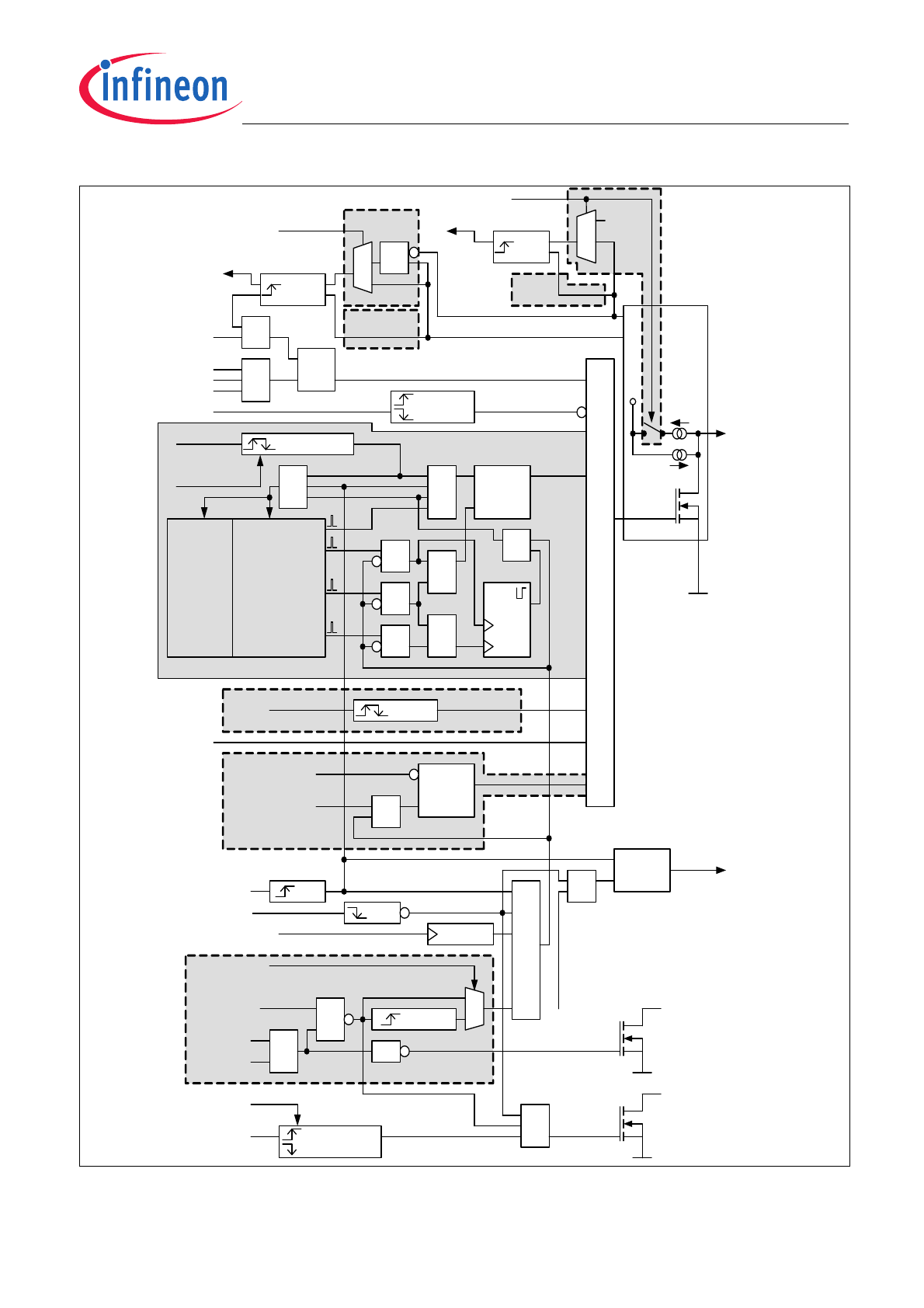
Figure 1
Output stages, functional schematic
&
n=15, 16
"Off"
"On, no delay "
"On, restart timeout "
"Keep State , restart
timeout“
DIS5_10
STAUS_UV
STATUS_OV
t
DIS5_10
T
OUTn _OTSD
MSC_MON
(timeout)
OUTn
ABE_STATUS
RST
V
DD
<V
DD_POR
t
DIAG_SCB
SCB
OUTn_SCB
n=5...10
OUTn_DIAC
n=
11
...
18
D
R
MSC downstream
OUTn
Control
Flipflop
OUTREG
≥1
DELAYIN
Lower thresholds
DELAYOUT
DELAYIN_CONFx
DELAYIN_FIL
OUTPUT_STBY
ABE_IMPACT
t
POR
t
DELRES
Discard
Restart
n=1...14, 17, 18
Output _Stages _Function _Overview.vsd
t
FIL_OFF_DEL
MU
X
SVBATT
t
MSC_MON
EXT_SCB
MU
X
OL
RES15_16
Higher thresholds
of DELAYIN
&
n=5...14
n=1…4, 15…18
MU
X
OUTn_DIA1/2
t
DIAG_OL
„0"
n=1…10
See „Block Diagramm V
DD
Monitoring“
t
RST
DELAYIN_FIL
OUTn_DIA1/2
t
DELAYIN_GLITCH_x
≥1
≥1
&
&
≥1
≥1
R
S
OUTn
Control
Flipflop
&
&
t
OUTn_OVSD
t
OUTn_OVSON
t
DELAYIN_GLITCH_x
t
DELAYIN_x
V
O
U
T
n_B
IA
S
&
Reset
≥1
OUTn_CONTROL
OUTn_DELAY
OUTn_SCB
OUTn_DIAC
S
R
Flip
Flop
RD_DATA
OFF/ON
≥1
WR_RST
≥1
ABE
&
&
Reset
STATUS_SVBATT
DIS5_10_STATUS
DELAYIN _STATUS
RES15_16_STATUS
D
R
POR
POR_FLAG
DIAREG
6.2
≥1
R
EAD
_D
IA
R
E
G
6
≥1
TLE 8718 SA
Block Diagram
Data Sheet
7
Rev. 1.1, 2012-07-31
2
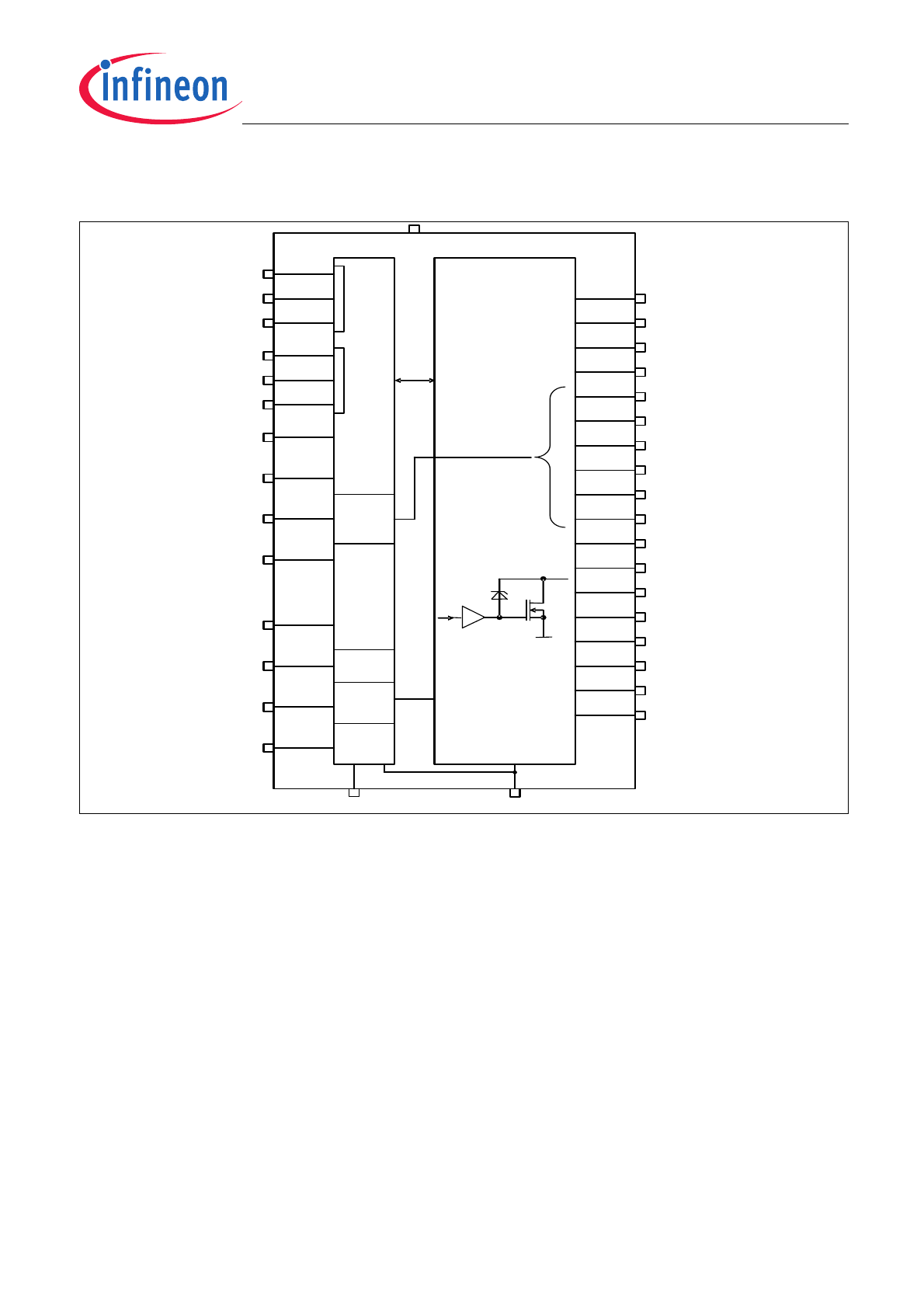
Block Diagram
Figure 2
Block Diagram
SIN
SIP
FCLP
FCLN
SSY
SDO
OUT1
M
ic
ro S
ec
on
d
C
han
ne
l
Reset
VDD
Monitoring
Power
Logic
8A/55V
GNDABE
ABE
RST
DIS5_10
SI
FCL
Enable
SVBATT
Block_Diagram.vsd
DELAYIN
DELAYOUT
Slug
OUT2
3A/55V
OUT3
8A/55V
OUT4
3A/55V
OUT5
2.2A/55V
OUT6
2.2A/55V
OUT7
2.2A/55V
OUT8
2.2A/55V
OUT9
2.2A/55V
OUT10
2.2A/55V
OUT11
2.2A/55V
OUT12
2.2A/55V
OUT13
2.2A/55V
OUT14
2.2A/55V
OUT15
0.6A/55V
OUT16
0.6A/55V
OUT17
0.6A/55V
OUT18
0.6A/55V
DE
LA
Y
IN/
O
U
T
Battery
Voltage
Monitoring
PGND
VDD
Data Sheet
8
Rev. 1.1, 2012-07-31
TLE 8718 SA
Pin Configuration
3
Pin Configuration
3.1
Pin Assignment
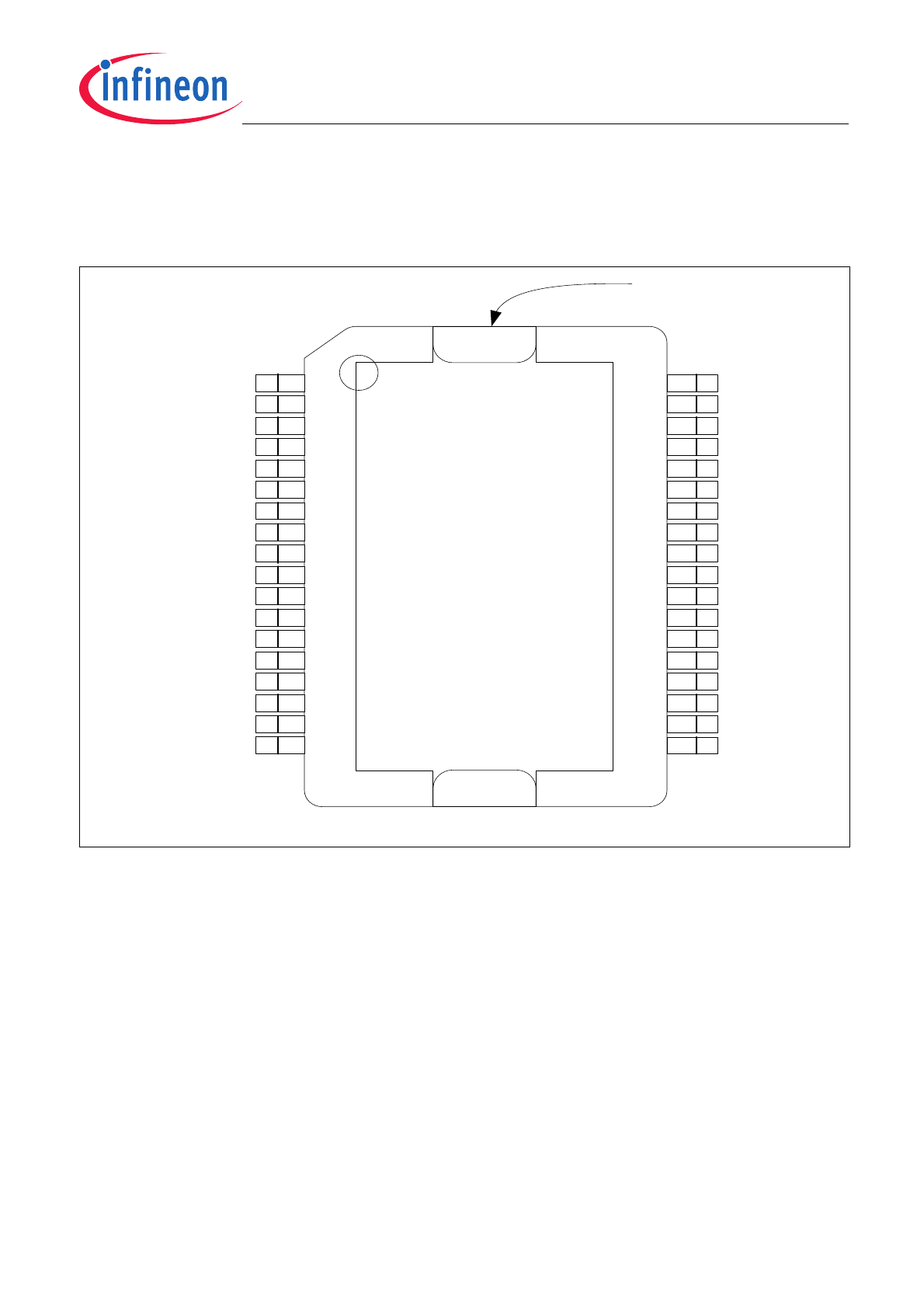
Figure 3
Pin Assignment
1
2
3
4
5
6
7
8
9
10
11
12
13
14
15
16
17
18
OUT1
OUT5
OUT9
SVBATT
ABE
GNDABE
VDD
OUT15
36
35
34
33
32
31
30
29
28
27
26
25
24
23
22
21
20
19
OUT2
OUT6
OUT14
OUT18
FCL
FCLN
FCLP
SI
SIP
SSY
SDO
RST
OUT16
OUT12
OUT8
OUT4
OUT10
OUT1
OUT13
OUT17
DELAYIN
DELAYOUT
DIS5_10
SIN
PGND
(Slug)
OUT11
OUT7
OUT3
OUT3
Pin_Config.vsd
TLE 8718 SA
Pin Configuration
Data Sheet
9
Rev. 1.1, 2012-07-31
3.2
Pin Definitions and Functions
Pin
Symbol
Function
1, 2
OUT1
1)
Drain Connection of Power stage.
Short circuit proof
Individually protected against overtemperature
diagnostic functions
control via MSC
Clamping of the output voltage by zener diodes
36
OUT2
17, 18
OUT3
2)
19
OUT4
3
OUT5
35
OUT6
16
OUT7
20
OUT8
4
OUT9
34
OUT10
15
OUT11
21
OUT12
5
OUT13
33
OUT14
14
OUT15
22
OUT16
6
OUT17
32
OUT18
9
DIS5_10
Disable pin for OUT5...OUT10 (low level disables OUT5...OUT10 after filtering time
(
t
DIS5_10
) has expired). The thresholds are defined in
Chapter 7
(active low, internal
pull-up)
7
DELAYIN
DELAYIN input (internal pull-down, active low): Disable pin for DELAYOUT after the
configurable filtering time (
t
DELAYIN
) has expired and Reset pin for OUT15 and OUT16.
The thresholds are defined in
Chapter 7
.
8
DELAYOUT
Open drain output generating active low level if DELAYIN is low level (below
V
DELAYIN_L
) and
t
DELYAIN
has expired, input ABE disables stages or
V
DD
monitoring has
detected a supply voltage failure. See
Chapter 7
.
11
ABE
Bidirectional pin (active low).
Indicates VDD overvoltage and undervoltage condition by pulling ABE-pin low.
If forced to low from externally all stages are turned off.
12
GNDABE
Sense ground. Reference ground for
V
DD
monitoring only. Connect this pin to ground.
13
VDD
Supply voltage 5V
24
SDO
MSC interface. Upstream data, open drain output
25
SSY
MSC interface. Chip select and synchronization strobe.
26
SIP
MSC interface. Downstream data positive for differential interface
27
SIN
MSC interface. Downstream data negative for differential interface
28
SI
MSC interface optional downstream data input for single ended interface
29
FCLP
MSC interface. Clock positive for differential interface
30
FCLN
MSC interface. Clock negative for differential interface
31
FCL
MSC interface optional clock input for single ended interface
Data Sheet
10
Rev. 1.1, 2012-07-31
TLE 8718 SA
Pin Configuration
3.3
Abbreviations
23
RST
Reset input (active low, internal pull-up). Shuts down all stages regardless of their
input signals. Clears the fault registers and resets the MSC interface registers
(partially).
10
SVBATT
Sense Battery Voltage Monitoring Pin. Connect to V
BAT
. Used to activate factory test
mode. See
Chapter 6.4
.
Slug
PGND
Power Ground. Internally used as PGND. Analogue circuits except VDD-monitoring
refer to PGND. Connect to Ground.
1) Pin1 and Pin2 have to be connected together without any parasitic resistor
2) Pin17 and Pin18 have to be connected together without any parasitic resistor in between.
Table 2
Abbreviations
ABE
“ABschaltung Endstufen” (switch off output stages)
C
Command bit
CD
Command data bit
DC
Don´t care bit
DOT
Diagnosis overtemperature
LVDS
Low voltage differential signal
MSC
Micro Second Channel
NCB
Number of bits of the active phase of a command frame
NDB
Number of bits of the active phase of a data frame
OL
Open Load (diagnostic stage information)
OTSD
Over Temperature Shut Down (threshold to shut down stages for device self
protection)
OTW
Over Temperature Warning (diagnostic information)
POR
Power On Reset, including filter time t
POR
PS
Power Stage(s)
RST
ReSeT input pin
SCB
Short Circuit to Battery (diagnostic stage information)
SCG
Short Circuit to Ground (diagnostic stage information)
SSY
Select / SYnc signal for MSC communication
SB
Selection bit
TC
Test coverage
UD
Upstream data bit
Pin
Symbol
Function