

Industrial & Multimarket
Data Sheet
Revision 2.0, 2012-06-14
ISO1I811T
Isolated 8 Channel Digital Input with IEC61131-2 Type 1/2/3 Characteristics
ISOFACE™

Edition 2012-06-14
Published by
Infineon Technologies AG
81726 Munich, Germany
©
2012
Infineon Technologies AG
All Rights Reserved.
Legal Disclaimer
The information given in this document shall in no event be regarded as a guarantee of conditions or
characteristics. With respect to any examples or hints given herein, any typical values stated herein and/or any
information regarding the application of the device, Infineon Technologies hereby disclaims any and all warranties
and liabilities of any kind, including without limitation, warranties of non-infringement of intellectual property rights
of any third party.
Information
For further information on technology, delivery terms and conditions and prices, please contact the nearest
Infineon Technologies Office (
www.infineon.com
).
Warnings
Due to technical requirements, components may contain dangerous substances. For information on the types in
question, please contact the nearest Infineon Technologies Office.
Infineon Technologies components may be used in life-support devices or systems only with the express written
approval of Infineon Technologies, if a failure of such components can reasonably be expected to cause the failure
of that life-support device or system or to affect the safety or effectiveness of that device or system. Life support
devices or systems are intended to be implanted in the human body or to support and/or maintain and sustain
and/or protect human life. If they fail, it is reasonable to assume that the health of the user or other persons may
be endangered.
Data Sheet
3
Revision 2.0, 2012-06-14
ISO1I811T
ISO1I811T
Revision History: 2012-06-14, Revision 2.0
Previous Version: Preliminary Data Sheet V1.0
Page
Subjects (major changes since last revision)
V2.0
Data Sheet
Page 25
Parallel Interface timing table updated
Page 26
Serial Interface timing table updated

ISO1I811T
Data Sheet
4
Revision 2.0, 2012-06-14
1
Pin Configuration and Functionality . . . . . . . . . . . . . . . . . . . . . . . . . . . . . . . . . . . . . . . . . . . . . . . . . 6
1.1
Pin Configuration . . . . . . . . . . . . . . . . . . . . . . . . . . . . . . . . . . . . . . . . . . . . . . . . . . . . . . . . . . . . . . . . . 6
1.2
Pin Functionality . . . . . . . . . . . . . . . . . . . . . . . . . . . . . . . . . . . . . . . . . . . . . . . . . . . . . . . . . . . . . . . . . . 8
1.2.1
Pins of Sensor Interface . . . . . . . . . . . . . . . . . . . . . . . . . . . . . . . . . . . . . . . . . . . . . . . . . . . . . . . . . . 8
1.2.2
Pins of Serial and Parallel logic Interface . . . . . . . . . . . . . . . . . . . . . . . . . . . . . . . . . . . . . . . . . . . . . 9
2
Blockdiagram . . . . . . . . . . . . . . . . . . . . . . . . . . . . . . . . . . . . . . . . . . . . . . . . . . . . . . . . . . . . . . . . . . 10
3
Functional Description . . . . . . . . . . . . . . . . . . . . . . . . . . . . . . . . . . . . . . . . . . . . . . . . . . . . . . . . . . . 11
3.1
Introduction . . . . . . . . . . . . . . . . . . . . . . . . . . . . . . . . . . . . . . . . . . . . . . . . . . . . . . . . . . . . . . . . . . . . . 11
3.2
Power Supply . . . . . . . . . . . . . . . . . . . . . . . . . . . . . . . . . . . . . . . . . . . . . . . . . . . . . . . . . . . . . . . . . . . 11
3.3
Internal Oscillator . . . . . . . . . . . . . . . . . . . . . . . . . . . . . . . . . . . . . . . . . . . . . . . . . . . . . . . . . . . . . . . . 12
3.4
Sensor Input . . . . . . . . . . . . . . . . . . . . . . . . . . . . . . . . . . . . . . . . . . . . . . . . . . . . . . . . . . . . . . . . . . . . 12
3.5
Common Error Output . . . . . . . . . . . . . . . . . . . . . . . . . . . . . . . . . . . . . . . . . . . . . . . . . . . . . . . . . . . . 14
3.6
Programmable Digital Input Filter . . . . . . . . . . . . . . . . . . . . . . . . . . . . . . . . . . . . . . . . . . . . . . . . . . . . 14
3.7
Parallel Interface Mode . . . . . . . . . . . . . . . . . . . . . . . . . . . . . . . . . . . . . . . . . . . . . . . . . . . . . . . . . . . . 15
3.8
Serial Interface Mode . . . . . . . . . . . . . . . . . . . . . . . . . . . . . . . . . . . . . . . . . . . . . . . . . . . . . . . . . . . . . 16
4
Standard Compliance . . . . . . . . . . . . . . . . . . . . . . . . . . . . . . . . . . . . . . . . . . . . . . . . . . . . . . . . . . . . 17
5
Electrical Characteristics . . . . . . . . . . . . . . . . . . . . . . . . . . . . . . . . . . . . . . . . . . . . . . . . . . . . . . . . . 19
5.1
Absolute Maximum Ratings . . . . . . . . . . . . . . . . . . . . . . . . . . . . . . . . . . . . . . . . . . . . . . . . . . . . . . . . 19
5.2
Operating Conditions and Power Supply . . . . . . . . . . . . . . . . . . . . . . . . . . . . . . . . . . . . . . . . . . . . . . 20
5.3
Electrical Characteristics Input Side . . . . . . . . . . . . . . . . . . . . . . . . . . . . . . . . . . . . . . . . . . . . . . . . . . 22
5.4
Electrical Characteristics Microcontroller Interface . . . . . . . . . . . . . . . . . . . . . . . . . . . . . . . . . . . . . . . 24
6
Package Outline . . . . . . . . . . . . . . . . . . . . . . . . . . . . . . . . . . . . . . . . . . . . . . . . . . . . . . . . . . . . . . . . 27
Data Sheet
5
Revision 2.0, 2012-06-14
ISO1I811T
Isolated 8 Channel Digital Input with
IEC61131-2 Type 1/2/3 Characteristics
Product Highlights
•
Minimization of power dissipation due to constant current
characteristic
•
Status LED output for each input
•
Digital averaging of the input signals to suppress interference
pulses
•
Isolation between Input and Output using Coreless
Transformer Technology
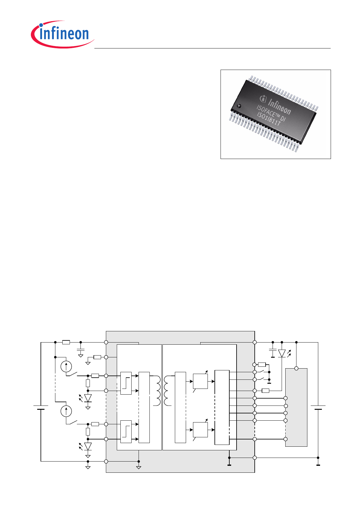
µC
e.g.
XE166
I0H
I0L
GNDBB
I7H
I7L
VBB
VCC
TS
/ERR
/CS
/RD
GND
S
E
R
I
A
L
I
Z
E
D
E
S
E
R
I
A
L
I
Z
E
L
O
G
I
C
ISO1I811T
parallel
or serial
interface
digital
filter
digital
filter
8 s
ens
or
s
2k
12k
330n
2k
12k
IN0
IN7
V
FI
GNDFI
DS0
DS1
Rosc
Features
•
Complete system integration (up to eight digital
sensor or switch inputs, galvanic isolation and
intelligent micro-controller or bus-ASIC interface)
•
8-channel input according to IEC61131-2 (Type
1/2/3)
•
Integrated galvanic isolation 500VAC
(EN60664-1, UL1577)
•
3.3/5V SPI and parallel micro-controller interface
•
Adjustable deglitching filters
•
Up to 125 kHz sampling frequency
•
V
BB
under-voltage detection
•
Package: TSSOP-48, 8 mm x 12.5 mm
Typical Application
Programmable Logic Controllers(PLC)
Industrial PC
General Control Equipment
Description
The ISO1I811T is an electrically isolated 8 bit data
input interface in TSSOP-48 package.
This part is used to detect the signal states of eight
independent input lines according to IEC61131-2 Type
1/2/3 (e.g. two-wire proximity switches) with a common
ground (GNDFI).
For operation in accordance with IEC61131-2, it is
necessary for the ISO1I811T to be wired with resistors
according to the application diagram.
The 8 bit parallel/serial µC compatible interface allows
the IC to directly connect to a µC system. The µC
interface also supports a direct control mode and is
designed to operate with 3.3/5V CMOS compatible
levels.
The data transfer and isolation from input to output side
is realized by the integrated Coreless Transformer
Technology.
ISO1I811T
Pin Configuration and Functionality
Data Sheet
6
Revision 2.0, 2012-06-14
1
Pin Configuration and Functionality
The pin configuration slightly differs for the parallel or the serial interface.
1.1
Pin Configuration
The ordering, type and functions of the IC pins are listed in the
Table 1
.
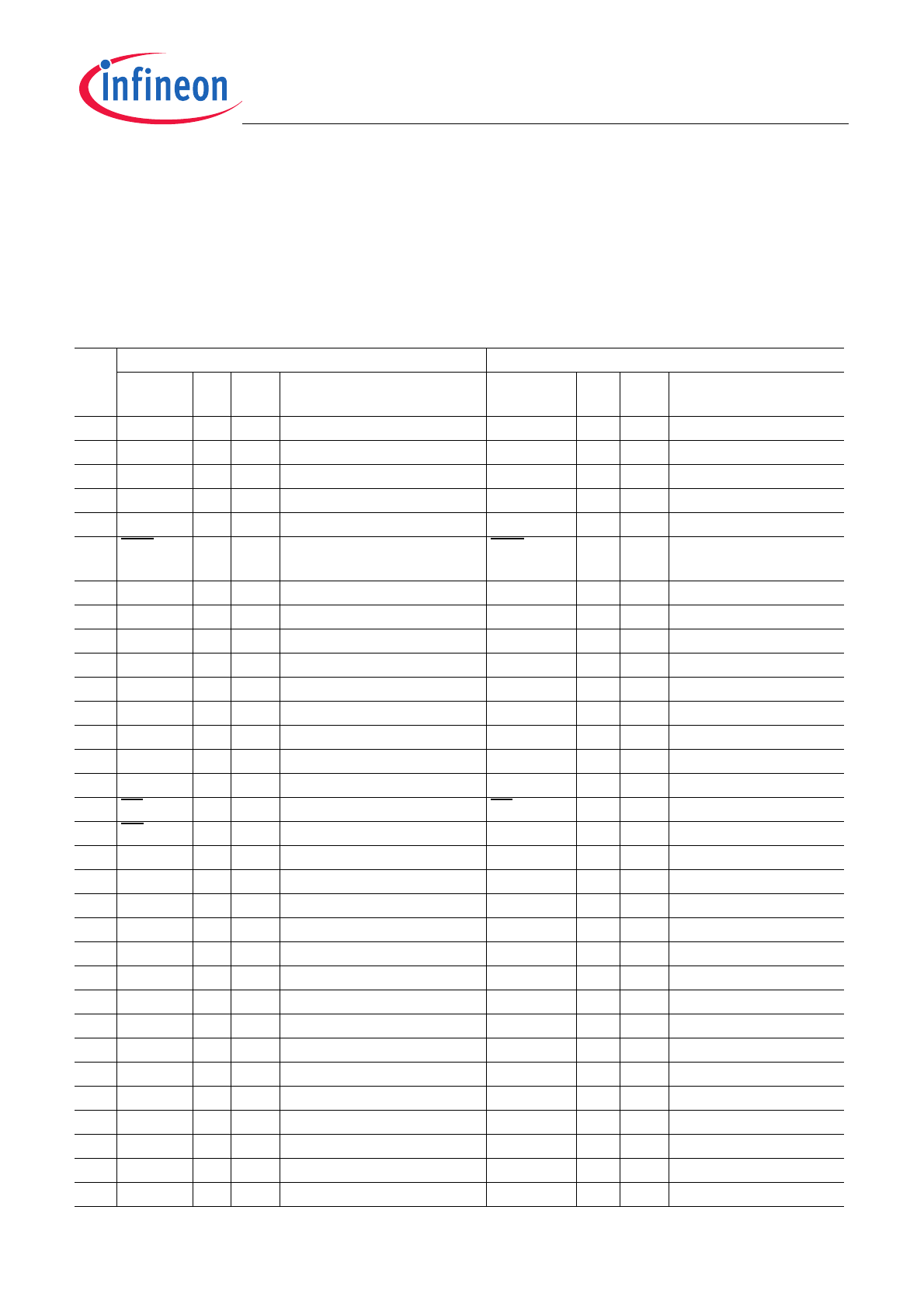
Table 1
Pin Configuration
Pin
Parallel Interface Mode
Serial Interface Mode
Symbol
Ctrl
1)
Type
2)
Function
Symbol
Ctrl. Type Function
1
GND
A
Logic Ground
GND
2
SEL
I
PU
Serial Parallel Mode Select
SEL
3
n.c.
not connected
n.c.
4
ROSC
A
Clock Frequency Adjustment ROSC
5
VCC
A
Positive 5/3.3V logic supply
VCC
6
ERR
O
OD,
PU
Error output
ERR
7
GND
A
Logic Ground
GND
8
D0
O
PPZ
Data output bit0
SDI
I
PD
SPI Data input
9
D1
O
PPZ
Data output bit1
GND
10
D2
O
PPZ
Data output bit2
GND
11
D3
O
PPZ
Data output bit3
GND
12
D4
O
PPZ
Data output bit4
GND
13
D5
O
PPZ
Data output bit5
SCLK
I
PD
SPI Shift Clock input
14
D6
O
PPZ
Data output bit6
GND
15
D7
O
PPZ
Data output bit7
SDO
O
PPZ
SPI Data output
16
CS
I
PU
Chip Select
CS
17
RD
I
PU
Data Read Input
n.c.
not connected
18
GND
A
Logic Ground
GND
19
DS0
I
PD
Filter Select Input 0
DS0
20
DS1
I
PD
Filter Select Input 1
DS1
21
GND
A
Logic Ground
GND
22
n.c.
not connected
n.c.
23
n.c.
not connected
n.c.
24
GND
A
Logic Ground
GND
25
GNDBB
A
Input Ground
GNDBB
26
VBB
A
Positive input supply voltage VBB
27
I0L
A
Input 0 Low, LED Out
I0L
28
I0H
A
Input 0 High
I0H
29
I1L
A
Input 1 Low, LED Out
I1L
30
I1H
A
Input 1 High
I1H
31
GNDBB
A
Input Ground
GNDBB
32
I2L
A
Input 2 Low, LED Out
I2L
Data Sheet
7
Revision 2.0, 2012-06-14
ISO1I811T
Pin Configuration and Functionality
33
I2H
A
Input 2 High
I2H
34
I3L
A
Input 3 Low, LED Out
I3L
35
I3H
A
Input 3 High
I3H
36
TS
A
Sensor Type 1/2/3 Select
TS
37
GNDBB
A
Input Ground
GNDBB
38
n.c.
not connected
n.c.
39
I4L
A
Input 4 Low, LED Out
I4L
40
I4H
A
Input 4 High
I4H
41
I5L
A
Input 5 Low, LED Out
I5L
42
I5H
A
Input 5 High
I5H
33
GNDBB
A
Input Ground
GNDBB
44
I6L
A
Input 6 Low, LED Out
I6L
45
I6H
A
Input 6 High
I6H
46
I7L
A
Input 7 Low, LED Out
I7L
47
I7H
A
Input 7 High
I7H
48
GNDBB
A
Input Ground
GNDBB
1) Direction of the pin: I = input, O = output, IO = Input/Output
2) Type of the pin: A = analog, OD = Open-Drain, PU = internal Pull-Up resistor, PD = internal Pull-Down resistor,
PPZ = Push-Pull pin with High-Impedance functionality
Table 1
Pin Configuration
Pin
Parallel Interface Mode
Serial Interface Mode
Symbol
Ctrl
1)
Type
2)
Function
Symbol
Ctrl. Type Function
ISO1I811T
Pin Configuration and Functionality
Data Sheet
8
Revision 2.0, 2012-06-14
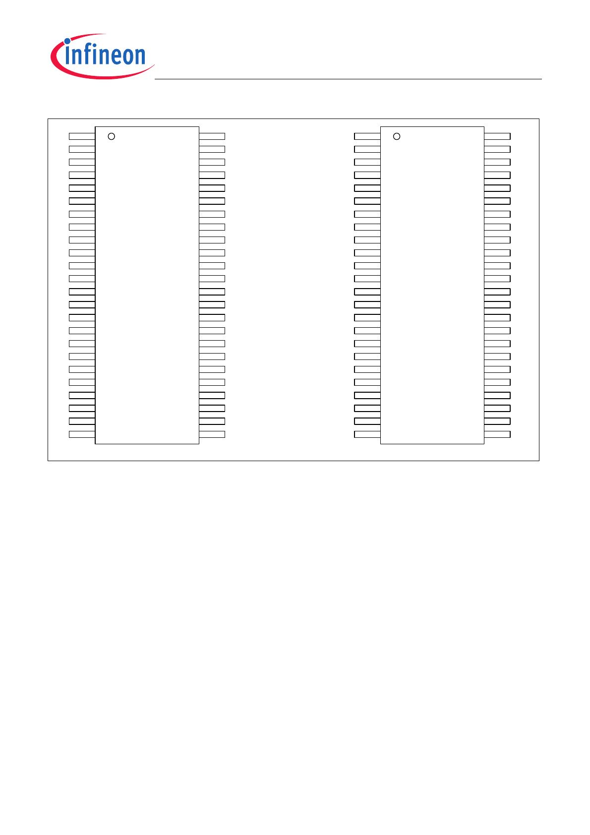
Figure 1
TSSOP-48 Pinout for Parallel and Serial Interface
1.2
Pin Functionality
The meaning and the functions of the IC pins are described below.
1.2.1
Pins of Sensor Interface
VBB (Positive supply 9.6-35V sensor supply)
VBB supplies the sensor input stage.
GNDBB (Ground for VBB domain)
This pin acts as the ground reference for the sensor input stage, that is supplied by VBB.
I0H... I7H (Input channel 0 ... 7)
Sensor inputs with current sink characteristic according IEC61131-2 Type 1/2/3 which has been selected by pin TS
I0L... I7L (LED output channel 0 ... 7)
This pin provides the output signal to switch on the LED if the input voltage and current has been detected as
“High” according the selected type.
TS (Type Select)
By connecting a resistor between TS and GNDBB the sensor type (Type 1/2/3) can be selected (refer to
Table 9
for corresponding resistor value). This pin is for static configuration (pin-strapping). The voltage level at pin TS is
not allowed to be changed during operation.
GND
SEL
n.c.
Rosc
/ERR
GND
D0
D1
D3
D4
D5
D6
D7
/CS
/RD
GND
D2
DS0
1
2
3
4
5
6
7
8
9
10
11
12
13
14
15
16
17
18
GNDBB
I6H
I6L
n.c.
I5H
I5L
I4H
GNDBB
GNDBB
I3H
I7H
I7L
I2H
I3L
I2L
I4L
TS
36
35
34
33
32
31
30
29
28
27
26
25
Pinout for parallel
Interface
DS1
VCC
GND
n.c.
n.c.
GND
19
20
21
22
23
24
I1H
I1L
I0L
I0H
VBB
GNDBB
44
43
42
41
40
39
38
37
48
47
46
45
1
2
3
4
5
6
7
8
9
10
11
12
13
14
15
16
17
18
36
35
34
33
32
31
30
29
28
27
26
25
Pinout for serial
Interface
19
20
21
22
23
24
44
43
42
41
40
39
38
37
48
47
46
45
GND
SEL
n.c.
Rosc
/ERR
GND
SDI
GND
GND
GND
SCLK
GND
SDO
/CS
n.c.
GND
GND
DS0
DS1
VCC
GND
n.c.
n.c.
GND
n.c. = Not Connected
GNDBB
GNDBB
I6H
I6L
n.c.
I5H
I5L
I4H
GNDBB
GNDBB
I3H
I7H
I7L
I2H
I3L
I2L
I4L
TS
I1H
I1L
I0L
I0H
VBB
GNDBB
GNDBB

Data Sheet
9
Revision 2.0, 2012-06-14
ISO1I811T
Pin Configuration and Functionality
1.2.2
Pins of Serial and Parallel logic Interface
Some pins are common for both interface types, some others are specific for the parallel or serial access.
VCC (Positive 3.3 / 5V logic supply)
VCC supplies the output interface that is electrically isolated from the sensor input stage. The interface can be
supplied with 3.3 / 5V.
GND (Ground for VCC domain)
This pin is the ground reference for the uC-interface that is supplied by VCC.
ROSC (Clock Adjustment)
A high precision resistor has to be connected between ROSC and GND to guarantee the frequency accuracy of
the sampling clock. For details see
Chapter 3.3
.
ERR (Error Output)
The low active ERR signal contains the OR-wired information of the sensor input missing voltage (MV) detection
and the internal data transmission failure detection unit. The output pin ERR provides an open drain functionality.
A current source is also connected to the pin ERR. In normal operation the signal ERR is high. See
Chapter 3.5
for more details.
DS0, DS1 (Filter Select)
The internal filter delay can be selected by pulling those pins to VCC or to GND (see
Table 10
). These pins are
for static configuration (pin-strapping).
CS (Chip Select)
When this pin is in a logic Low state, the IC interface is enabled and data can be transferred.
SEL (Serial or Parallel Mode Select)
When this pin is in a logic High state, the IC operates in Serial Mode. For Parallel Mode operation the pin has to
be pulled into logic Low state. This pin has an internal Pull-UP resistor.
The following pins are provided by the parallel interface
D7:D0 (Data output bit7 ... bit0)
The pins D0 .. D7 are the outputs for data read.
RD (Read Select)
By pulling this pin down, a read transaction is initiated on the data bus and the data becomes valid.
The following pins are provided by the serial interface
SCLK (Serial interface shift clock)
Output data is updated with the falling edge of this input clock signal.
SDI (Serial interface input data)
SDI is put into a FIFO dedicated to the sensor data bits (no internal registers Write operation supported, only daisy
chain). Input data is sampled with the rising edge of SCLK.
SDO (Serial interface data)
SDO provides the sensor data bits.
ISO1I811T
Blockdiagram
Data Sheet
10
Revision 2.0, 2012-06-14
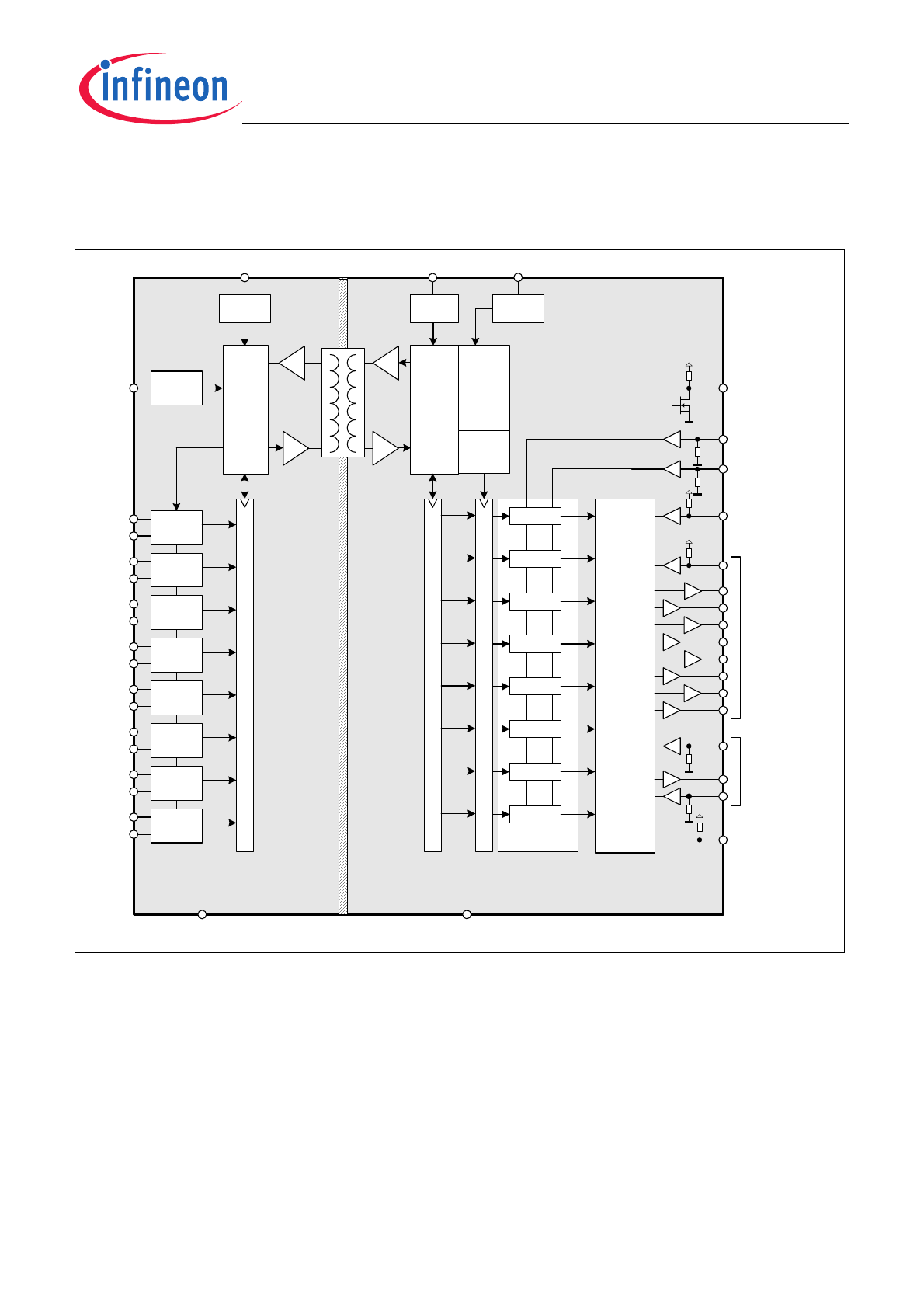
2
Blockdiagram
Figure 2
Block Diagram
I1H
I1L
I2H
I2L
I3H
I3L
I4H
I4L
I5H
I5L
I6H
I6L
I7H
I7L
Sensor
Circuit 0
I0H
I0L
GNDBB
DATA
DATA
DATA
DATA
DATA
DATA
DATA
DATA
S
E
R
I
A
L
I
Z
E
MV
D
E
S
E
R
I
A
L
I
Z
E
U
P
D
A
T
E
G
A
T
E
/ERR
Interface
Handler
/CS
/RD
SDI
D7
D6
D5
D4
D3
D2
D1
D0
SCLK
SDO
parallel
interface
serial
interface
GND
UVLO
VCC
Vali-
dation
UVLO
VBB
TX/RX
Control
TS
Type
Selector
Sensor
Circuit 1
Sensor
Circuit 2
Sensor
Circuit 3
Sensor
Circuit 4
Sensor
Circuit 5
Sensor
Circuit 6
Sensor
Circuit 7
DS0
TX/RX
Control
DATA
DATA
DATA
DATA
DATA
DATA
DATA
DATA
Filter 7
Filter 6
Filter 5
Filter 4
Filter 3
Filter 2
Filter 1
Filter 0
Startup
Common
Error
OSC
CLK
ROSC
DS1
SEL