

Sense and Control
Datasheet
Rev1.1, 2010-08-02
TLV4946K, TLV4946-2K
Value Optimized Hall Effect Latches for Industrial and Consumer
Applications

Edition 2010-08-02
Published by
Infineon Technologies AG
81726 Munich, Germany
©
2010
Infineon Technologies AG
All Rights Reserved.
Legal Disclaimer
The information given in this document shall in no event be regarded as a guarantee of conditions or
characteristics. With respect to any examples or hints given herein, any typical values stated herein and/or any
information regarding the application of the device, Infineon Technologies hereby disclaims any and all warranties
and liabilities of any kind, including without limitation, warranties of non-infringement of intellectual property rights
of any third party.
Information
For further information on technology, delivery terms and conditions and prices, please contact the nearest
Infineon Technologies Office (
www.infineon.com
).
Warnings
Due to technical requirements, components may contain dangerous substances. For information on the types in
question, please contact the nearest Infineon Technologies Office.
Infineon Technologies components may be used in life-support devices or systems only with the express written
approval of Infineon Technologies, if a failure of such components can reasonably be expected to cause the failure
of that life-support device or system or to affect the safety or effectiveness of that device or system. Life support
devices or systems are intended to be implanted in the human body or to support and/or maintain and sustain
and/or protect human life. If they fail, it is reasonable to assume that the health of the user or other persons may
be endangered.

TLV4946K, TLV4946-2K
Datasheet
3
Rev1.1, 2010-08-02
Value Optimized Hall Effect Latches for Industrial and Consumer Applications
Revision History: 2010-08-02, Rev1.1
Previous Revisions: 1.0
Page
Subjects (major changes since last revision)
all
TLV4946-2L removed
We Listen to Your Comments
Any information within this document that you feel is wrong, unclear or missing at all?
Your feedback will help us to continuously improve the quality of this document.
Please send your proposal (including a reference to this document) to:
sensors@infineon.com

TLV4946K, TLV4946-2K
Table of Contents
Datasheet
4
Rev1.1, 2010-08-02
Table of Contents . . . . . . . . . . . . . . . . . . . . . . . . . . . . . . . . . . . . . . . . . . . . . . . . . . . . . . . . . . . . . . . . 4
List of Figures . . . . . . . . . . . . . . . . . . . . . . . . . . . . . . . . . . . . . . . . . . . . . . . . . . . . . . . . . . . . . . . . . . . 5
List of Tables . . . . . . . . . . . . . . . . . . . . . . . . . . . . . . . . . . . . . . . . . . . . . . . . . . . . . . . . . . . . . . . . . . . . 6
1
Product Description . . . . . . . . . . . . . . . . . . . . . . . . . . . . . . . . . . . . . . . . . . . . . . . . . . . . . . . . . . . . . . 7
1.1
Overview . . . . . . . . . . . . . . . . . . . . . . . . . . . . . . . . . . . . . . . . . . . . . . . . . . . . . . . . . . . . . . . . . . . . . . . . 7
1.2
Features . . . . . . . . . . . . . . . . . . . . . . . . . . . . . . . . . . . . . . . . . . . . . . . . . . . . . . . . . . . . . . . . . . . . . . . . 7
1.3
Target Applications . . . . . . . . . . . . . . . . . . . . . . . . . . . . . . . . . . . . . . . . . . . . . . . . . . . . . . . . . . . . . . . . 7
2
Functional Description . . . . . . . . . . . . . . . . . . . . . . . . . . . . . . . . . . . . . . . . . . . . . . . . . . . . . . . . . . . . 8
2.1
General . . . . . . . . . . . . . . . . . . . . . . . . . . . . . . . . . . . . . . . . . . . . . . . . . . . . . . . . . . . . . . . . . . . . . . . . . 8
2.2
Pin Configuration . . . . . . . . . . . . . . . . . . . . . . . . . . . . . . . . . . . . . . . . . . . . . . . . . . . . . . . . . . . . . . . . . 8
2.3
Pin Description . . . . . . . . . . . . . . . . . . . . . . . . . . . . . . . . . . . . . . . . . . . . . . . . . . . . . . . . . . . . . . . . . . . 9
2.4
Block Diagram . . . . . . . . . . . . . . . . . . . . . . . . . . . . . . . . . . . . . . . . . . . . . . . . . . . . . . . . . . . . . . . . . . . 9
2.5
Operating Modes and States . . . . . . . . . . . . . . . . . . . . . . . . . . . . . . . . . . . . . . . . . . . . . . . . . . . . . . . 10
2.6
Functional Block Description . . . . . . . . . . . . . . . . . . . . . . . . . . . . . . . . . . . . . . . . . . . . . . . . . . . . . . . 10
3
Specification . . . . . . . . . . . . . . . . . . . . . . . . . . . . . . . . . . . . . . . . . . . . . . . . . . . . . . . . . . . . . . . . . . . 11
3.1
Application circuit . . . . . . . . . . . . . . . . . . . . . . . . . . . . . . . . . . . . . . . . . . . . . . . . . . . . . . . . . . . . . . . . 11
3.2
Absolute Maximum Ratings . . . . . . . . . . . . . . . . . . . . . . . . . . . . . . . . . . . . . . . . . . . . . . . . . . . . . . . . 11
3.3
Operating Range . . . . . . . . . . . . . . . . . . . . . . . . . . . . . . . . . . . . . . . . . . . . . . . . . . . . . . . . . . . . . . . . 12
3.4
Electrical Characteristics . . . . . . . . . . . . . . . . . . . . . . . . . . . . . . . . . . . . . . . . . . . . . . . . . . . . . . . . . . 12
4
Package Information . . . . . . . . . . . . . . . . . . . . . . . . . . . . . . . . . . . . . . . . . . . . . . . . . . . . . . . . . . . . 14
4.1
TLV4946K and TLV4946-2K Package Outline . . . . . . . . . . . . . . . . . . . . . . . . . . . . . . . . . . . . . . . . . . 14
Table of Contents

TLV4946K, TLV4946-2K
List of Figures
Datasheet
5
Rev1.1, 2010-08-02
Figure 1
Pin Configuration and sensitive area (Top view, figure not to scale) . . . . . . . . . . . . . . . . . . . . . . . . 8
Figure 2
TLV4946K, TLV4946-2K Block Diagram . . . . . . . . . . . . . . . . . . . . . . . . . . . . . . . . . . . . . . . . . . . . . 9
Figure 3
Definition of the Magnetic Field direction . . . . . . . . . . . . . . . . . . . . . . . . . . . . . . . . . . . . . . . . . . . . 10
Figure 4
Output Signal . . . . . . . . . . . . . . . . . . . . . . . . . . . . . . . . . . . . . . . . . . . . . . . . . . . . . . . . . . . . . . . . . 10
Figure 5
Application circuit . . . . . . . . . . . . . . . . . . . . . . . . . . . . . . . . . . . . . . . . . . . . . . . . . . . . . . . . . . . . . . 11
Figure 6
Timing Diagram . . . . . . . . . . . . . . . . . . . . . . . . . . . . . . . . . . . . . . . . . . . . . . . . . . . . . . . . . . . . . . . 13
Figure 7
Marking of the TLV4946K and TLV4946-2K and distance of the chip to the upper side . . . . . . . . 14
Figure 8
PG-SC59-3-5 Package Outline. . . . . . . . . . . . . . . . . . . . . . . . . . . . . . . . . . . . . . . . . . . . . . . . . . . . 14
Figure 9
Footprint PG-SC59-3-5 (SOT23 compatible) . . . . . . . . . . . . . . . . . . . . . . . . . . . . . . . . . . . . . . . . . 15
List of Figures

TLV4946K, TLV4946-2K
List of Tables
Datasheet
6
Rev1.1, 2010-08-02
Table 1
PIN Definitions for the PG-SC59-3-5 package . . . . . . . . . . . . . . . . . . . . . . . . . . . . . . . . . . . . . . . . 9
Table 2
Absolute Maximum Ratings . . . . . . . . . . . . . . . . . . . . . . . . . . . . . . . . . . . . . . . . . . . . . . . . . . . . . . 11
Table 3
Operating Range . . . . . . . . . . . . . . . . . . . . . . . . . . . . . . . . . . . . . . . . . . . . . . . . . . . . . . . . . . . . . . 12
Table 4
Electrical Characteristics . . . . . . . . . . . . . . . . . . . . . . . . . . . . . . . . . . . . . . . . . . . . . . . . . . . . . . . . 12
Table 5
Magnetic Characteristics . . . . . . . . . . . . . . . . . . . . . . . . . . . . . . . . . . . . . . . . . . . . . . . . . . . . . . . . 13
List of Tables
Product Name
Product Type
Order Code
Package
TLV4946K
Hall Effect Latch
SP000604402
PG-SC59-3-5
TLV4946-2K
Hall Effect latch
SP000604332
PG-SC59-3-5
High Precision Hall Effect Latch
TLV4946K, TLV4946-2K
Datasheet
7
Rev1.1, 2010-08-02
1
Product Description
1.1
Overview
The TLV4946K and TLV4946-2K are high precision Hall Effect Latches
with highly accurate switching thresholds for ambient operating
temperatures up to 85°C.
The TLV4946K and the TLV4946-2K are available in a lead-free and
halogen-free SMD package PG-SC59-3-5 package to meet current and
future requirements.
1.2
Features
•
2.7 V to 18 V supply voltage operation.
•
Operation from unregulated power supply.
•
High sensitivity and high stability of the magnetic switching points.
•
High resistance to mechanical stress by active error compensation.
•
Reverse battery protection (-18 V).
•
Superior temperature stability.
•
Low jitter (typically 1 µs).
•
High ESD performance (
± 4 kV HBM).
•
Digital output signal (open-drain).
•
Lead-free and halogen free SMD package
•
Not suitable for automotive applications
1.3
Target Applications
The TLV4946-2K is ideally suited to detect the rotor position in Brushless DC (BLDC) Motors used in industrial
and consumer applications, such as: air conditioning systems, pumps, washing machines, DVD players, rolling
shutter, etc. The TLV4946K can be used in index counting applications with a magnetized pole wheel mounted on
the axle of a motor.
TLV4946K, TLV4946-2K
Functional Description
Datasheet
8
Rev1.1, 2010-08-02
2
Functional Description
2.1
General
Precise magnetic switching thresholds and high temperature stability are achieved by active compensation circuits
and chopper techniques on chip. Offset voltages generated by temperature-induced stress or overmolding are
canceled so that high accuracy is achieved. The IC has an open collector output stage with 20 mA current sink
capability. A wide operating voltage range from 2.7 V to 18 V with reverse polarity protection down to -18 V makes
the TLV4946K and TLV4946-2K suitable for a wide range of applications. A magnetic south pole with a field
strength above B
op
turns the output on. A magnetic north pole exceeding B
rp
turns it off.
2.2
Pin Configuration
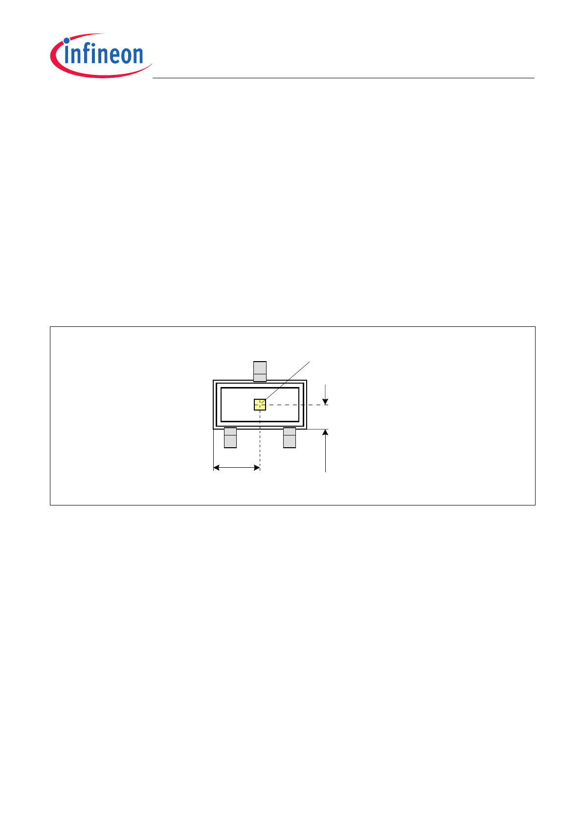
Figure 1
Pin Configuration and sensitive area (Top view, figure not to scale)
Center of
Sensitive Area
1
± 0.15
1.5
± 0.15
0.8
2
3
SC59
TLV4946K, TLV4946-2K
Functional Description
Datasheet
9
Rev1.1, 2010-08-02
2.3
Pin Description
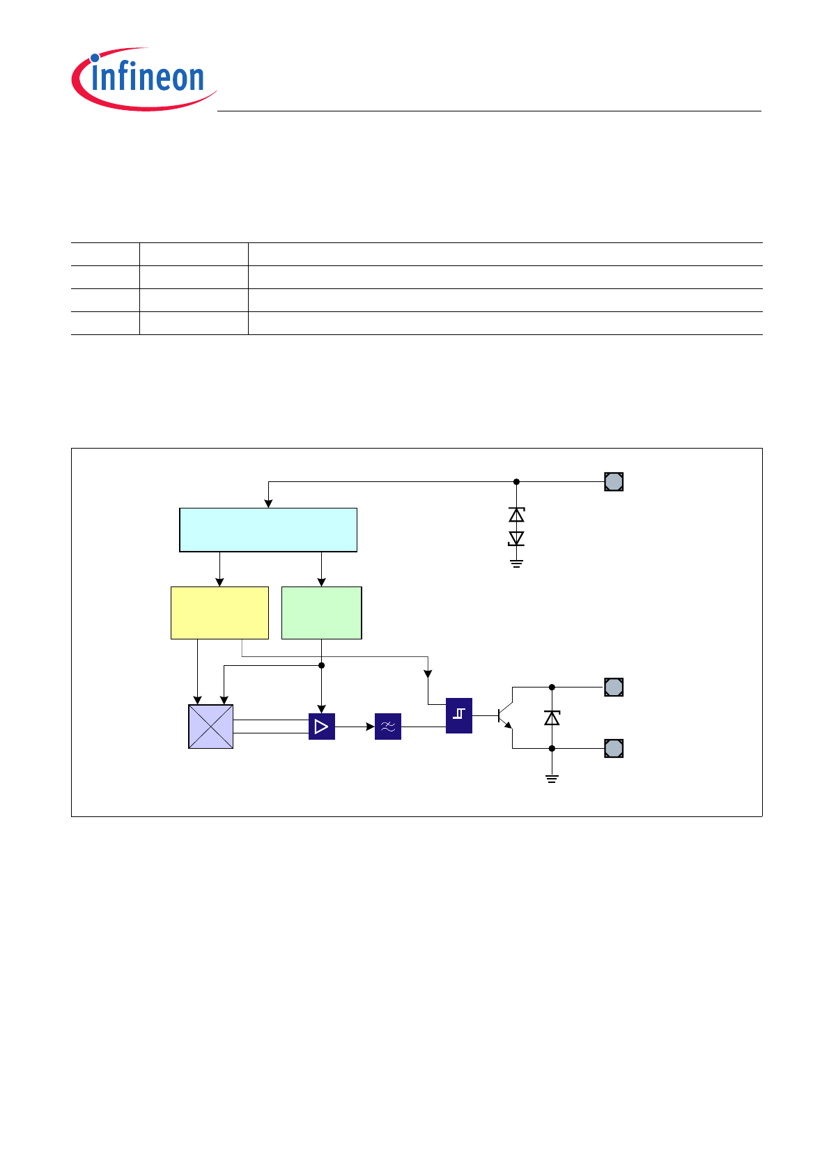
2.4
Block Diagram
Figure 2
TLV4946K, TLV4946-2K Block Diagram
Table 1
PIN Definitions for the PG-SC59-3-5 package
PIN No.
Name
Function
1
V
s
Supply Voltage
2
Q
Output
3
GND
Ground
Ref
Chopped
Hall Probe
V
S
Q
GND
Amplifier
Low
Pass
Filter
Comparator
with
Hysteresis
Voltage Regulator
reverse polarity protected
Oscillator
and
Sequencer
Bias and
Compensation
Circuits
TLV4946K, TLV4946-2K
Functional Description
Datasheet
10
Rev1.1, 2010-08-02
2.5
Operating Modes and States
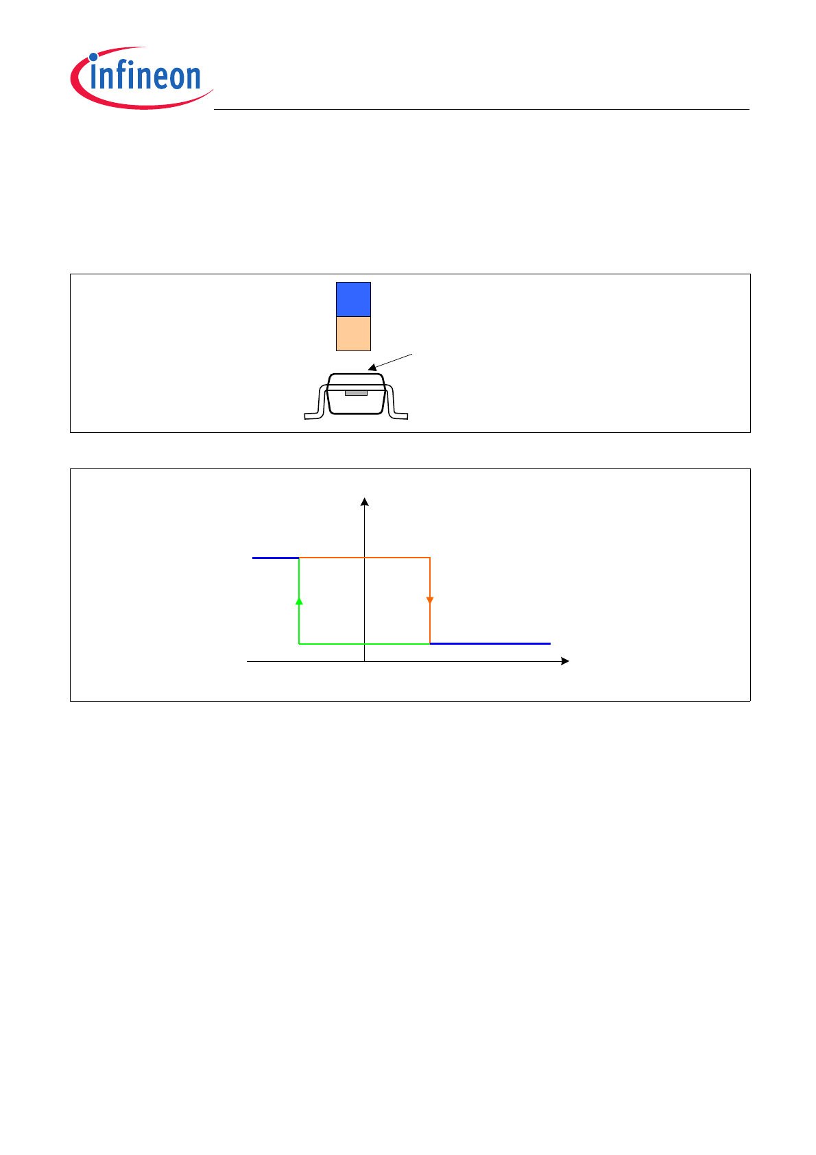
Field Direction and Definition
Positive magnetic fields correspond to the south pole of the magnet targeting the branded side of the package.
Figure 3
Definition of the Magnetic Field direction
Figure 4
Output Signal
2.6
Functional Block Description
The chopped Hall Effect Latch comprises a Hall probe, a bias generator, compensation circuits, an oscillator and
an output transistor. The bias generator provides currents to the Hall probe and the active circuits. Compensation
circuits stabilize response of the IC over temperature and reduce the impact of process variations.
The Active Error Compensation rejects offsets in the signal path and reduces the impact of mechanical stress in
the package caused by molding, soldering and thermal effects.
The chopper technique together with the threshold generator and the comparator ensure high accurate magnetic
switching points.
Branded Side
N
S
V
Q
B
op
B
rp
0
B