

TLE8242-2
8 Channel Fixed Frequency Constant Current
Control With Current Profile Detection
Data Sheet, Rev. 1.0, Feb 2010
Automotive Power

Data Sheet
2
Rev. 1.0, 2010-02-09
TLE8242-2
Table of Contents
Table of Contents . . . . . . . . . . . . . . . . . . . . . . . . . . . . . . . . . . . . . . . . . . . . . . . . . . . . . . . . . . . . . . . . 2
1
Overview . . . . . . . . . . . . . . . . . . . . . . . . . . . . . . . . . . . . . . . . . . . . . . . . . . . . . . . . . . . . . . . . . . . . . . . 4
1.1
Features . . . . . . . . . . . . . . . . . . . . . . . . . . . . . . . . . . . . . . . . . . . . . . . . . . . . . . . . . . . . . . . . . . . . . . . . 4
1.2
Applications . . . . . . . . . . . . . . . . . . . . . . . . . . . . . . . . . . . . . . . . . . . . . . . . . . . . . . . . . . . . . . . . . . . . . 5
1.3
General Description . . . . . . . . . . . . . . . . . . . . . . . . . . . . . . . . . . . . . . . . . . . . . . . . . . . . . . . . . . . . . . . 5
1.3.1
Direct PWM Mode Operation . . . . . . . . . . . . . . . . . . . . . . . . . . . . . . . . . . . . . . . . . . . . . . . . . . . . . . . 5
1.3.2
Constant Current Mode Operation . . . . . . . . . . . . . . . . . . . . . . . . . . . . . . . . . . . . . . . . . . . . . . . . . . . 6
2
Block Diagram . . . . . . . . . . . . . . . . . . . . . . . . . . . . . . . . . . . . . . . . . . . . . . . . . . . . . . . . . . . . . . . . . . 10
3
Pin Configuration . . . . . . . . . . . . . . . . . . . . . . . . . . . . . . . . . . . . . . . . . . . . . . . . . . . . . . . . . . . . . . . 11
3.1
Pin Assignment . . . . . . . . . . . . . . . . . . . . . . . . . . . . . . . . . . . . . . . . . . . . . . . . . . . . . . . . . . . . . . . . . 11
3.2
Pin Definitions and Functions . . . . . . . . . . . . . . . . . . . . . . . . . . . . . . . . . . . . . . . . . . . . . . . . . . . . . 11
4
General Product Characteristics . . . . . . . . . . . . . . . . . . . . . . . . . . . . . . . . . . . . . . . . . . . . . . . . . . . 15
4.1
Maximum Ratings . . . . . . . . . . . . . . . . . . . . . . . . . . . . . . . . . . . . . . . . . . . . . . . . . . . . . . . . . . . . . . . . 15
4.2
Functional Range . . . . . . . . . . . . . . . . . . . . . . . . . . . . . . . . . . . . . . . . . . . . . . . . . . . . . . . . . . . . . . . . 16
4.3
Thermal Resistance . . . . . . . . . . . . . . . . . . . . . . . . . . . . . . . . . . . . . . . . . . . . . . . . . . . . . . . . . . . . . . 16
5
Functional Description and Electrical Characteristics . . . . . . . . . . . . . . . . . . . . . . . . . . . . . . . . . 17
5.1
Supply and Reference . . . . . . . . . . . . . . . . . . . . . . . . . . . . . . . . . . . . . . . . . . . . . . . . . . . . . . . . . . . . 17
5.2
Input / Output . . . . . . . . . . . . . . . . . . . . . . . . . . . . . . . . . . . . . . . . . . . . . . . . . . . . . . . . . . . . . . . . . . . 18
5.3
Diagnostics . . . . . . . . . . . . . . . . . . . . . . . . . . . . . . . . . . . . . . . . . . . . . . . . . . . . . . . . . . . . . . . . . . . . . 20
5.3.1
On-State Diagnostics . . . . . . . . . . . . . . . . . . . . . . . . . . . . . . . . . . . . . . . . . . . . . . . . . . . . . . . . . . . . 22
5.3.2
Off-State Diagnostics . . . . . . . . . . . . . . . . . . . . . . . . . . . . . . . . . . . . . . . . . . . . . . . . . . . . . . . . . . . . 24
5.4
Output Driver . . . . . . . . . . . . . . . . . . . . . . . . . . . . . . . . . . . . . . . . . . . . . . . . . . . . . . . . . . . . . . . . . . . 28
5.5
Current Control . . . . . . . . . . . . . . . . . . . . . . . . . . . . . . . . . . . . . . . . . . . . . . . . . . . . . . . . . . . . . . . . . . 28
5.6
Current Feedback Registers . . . . . . . . . . . . . . . . . . . . . . . . . . . . . . . . . . . . . . . . . . . . . . . . . . . . . . . . 29
5.7
Direct PWM control . . . . . . . . . . . . . . . . . . . . . . . . . . . . . . . . . . . . . . . . . . . . . . . . . . . . . . . . . . . . . . . 30
5.7.1
Selecting the Frequency of Operation . . . . . . . . . . . . . . . . . . . . . . . . . . . . . . . . . . . . . . . . . . . . . . . 30
5.7.2
Selecting the Duty Cycle . . . . . . . . . . . . . . . . . . . . . . . . . . . . . . . . . . . . . . . . . . . . . . . . . . . . . . . . . 30
5.8
Current Profile Detection . . . . . . . . . . . . . . . . . . . . . . . . . . . . . . . . . . . . . . . . . . . . . . . . . . . . . . . . . . 31
5.8.1
Zone 1 . . . . . . . . . . . . . . . . . . . . . . . . . . . . . . . . . . . . . . . . . . . . . . . . . . . . . . . . . . . . . . . . . . . . . . . 33
5.8.2
Zone 2 . . . . . . . . . . . . . . . . . . . . . . . . . . . . . . . . . . . . . . . . . . . . . . . . . . . . . . . . . . . . . . . . . . . . . . . 33
5.8.3
Zone 3 . . . . . . . . . . . . . . . . . . . . . . . . . . . . . . . . . . . . . . . . . . . . . . . . . . . . . . . . . . . . . . . . . . . . . . . 33
5.8.4
Current Profile Time out & Detection Interrupted . . . . . . . . . . . . . . . . . . . . . . . . . . . . . . . . . . . . . . . 34
5.9
Serial Peripheral Interface (SPI) . . . . . . . . . . . . . . . . . . . . . . . . . . . . . . . . . . . . . . . . . . . . . . . . . . . . . 35
5.9.1
SPI Signal Description . . . . . . . . . . . . . . . . . . . . . . . . . . . . . . . . . . . . . . . . . . . . . . . . . . . . . . . . . . . 36
5.9.2
SPI Message Structure . . . . . . . . . . . . . . . . . . . . . . . . . . . . . . . . . . . . . . . . . . . . . . . . . . . . . . . . . . 38
5.9.2.1
SPI Message #0 - IC Version / Manufacturer . . . . . . . . . . . . . . . . . . . . . . . . . . . . . . . . . . . . . . . 38
5.9.2.2
SPI Message #1 - Control Method and Fault Mask Configuration . . . . . . . . . . . . . . . . . . . . . . . . 39
5.9.2.3
SPI Message #2 - Diagnostic Configuration (channel 0-3) . . . . . . . . . . . . . . . . . . . . . . . . . . . . . 41
5.9.2.4
SPI Message #3 - Diagnostic Configuration (channel 4-7) . . . . . . . . . . . . . . . . . . . . . . . . . . . . . 43
5.9.2.5
SPI Message #4 - Diagnostic Read (channel 0-3) . . . . . . . . . . . . . . . . . . . . . . . . . . . . . . . . . . . . 45
5.9.2.6
SPI Message #5 - Diagnostic Read (channel 4-7) . . . . . . . . . . . . . . . . . . . . . . . . . . . . . . . . . . . . 46
5.9.2.7
SPI Message #6 - PWM Offset (channel 0-3) . . . . . . . . . . . . . . . . . . . . . . . . . . . . . . . . . . . . . . . 47
5.9.2.8
SPI Message #7 - PWM Offset (channel 4-7) . . . . . . . . . . . . . . . . . . . . . . . . . . . . . . . . . . . . . . . 49
5.9.2.9
SPI Message #8 - Main Period Set . . . . . . . . . . . . . . . . . . . . . . . . . . . . . . . . . . . . . . . . . . . . . . . 51
5.9.2.10
SPI Message #9 - Control Variable Set (KP and KI) . . . . . . . . . . . . . . . . . . . . . . . . . . . . . . . . . . 53
5.9.2.11
SPI Message #10 - Current and Dither Amplitude Set . . . . . . . . . . . . . . . . . . . . . . . . . . . . . . . . 54
5.9.2.12
SPI Message #11 - Dither Period Set . . . . . . . . . . . . . . . . . . . . . . . . . . . . . . . . . . . . . . . . . . . . . 56
Table of Contents

Data Sheet
3
Rev. 1.0, 2010-02-09
TLE8242-2
Table of Contents
5.9.2.13
SPI Message #12 - Max / Min Current Read . . . . . . . . . . . . . . . . . . . . . . . . . . . . . . . . . . . . . . . . 58
5.9.2.14
SPI Message #13 - Average Current Read Over Dither Period . . . . . . . . . . . . . . . . . . . . . . . . . 60
5.9.2.15
SPI Message #14 - Autozero Trigger / Read . . . . . . . . . . . . . . . . . . . . . . . . . . . . . . . . . . . . . . . . 62
5.9.2.16
SPI Message #15 - PWM Duty Cycle . . . . . . . . . . . . . . . . . . . . . . . . . . . . . . . . . . . . . . . . . . . . . 64
5.9.2.17
SPI Message #16 - Current Profile Detection Setup 1 . . . . . . . . . . . . . . . . . . . . . . . . . . . . . . . . 66
5.9.2.18
SPI Message #17 - Current Profile Detection Setup 2 . . . . . . . . . . . . . . . . . . . . . . . . . . . . . . . . 68
5.9.2.19
SPI Message #18 - Current Profile Detection Feedback . . . . . . . . . . . . . . . . . . . . . . . . . . . . . . . 70
5.9.2.20
SPI Message #19 - Read Generic Flag Bits . . . . . . . . . . . . . . . . . . . . . . . . . . . . . . . . . . . . . . . . 72
6
Application Information . . . . . . . . . . . . . . . . . . . . . . . . . . . . . . . . . . . . . . . . . . . . . . . . . . . . . . . . . . 74
6.1
Further Application Information . . . . . . . . . . . . . . . . . . . . . . . . . . . . . . . . . . . . . . . . . . . . . . . . . . . . . . 74
7
Package Outlines . . . . . . . . . . . . . . . . . . . . . . . . . . . . . . . . . . . . . . . . . . . . . . . . . . . . . . . . . . . . . . . 75
8
Revision History . . . . . . . . . . . . . . . . . . . . . . . . . . . . . . . . . . . . . . . . . . . . . . . . . . . . . . . . . . . . . . . . 77
PG-LQFP-64
Type
Package
Marking
TLE8242-2
PG-LQFP-64
TLE8242-2L
Data Sheet
4
Rev. 1.0, 2010-02-09
8 Channel Fixed Frequency Constant Current Control
With Current Profile Detection
TLE8242-2
1
Overview
1.1
Features
•
Low side constant current control pre-driver integrated circuit
•
Eight independent channels
•
Output current programmable with 11 bit resolution
– Current range = 0 to 1.2A (typ) with a 0.2
Ω sense resistor
– Resolution = 0.78125 mA/bit (typ) with a 0.2
Ω sense resistor
– +/- 2% full scale error over temperature when autozero is used
•
Programmable PWM frequency via SPI from approximately
10 Hz to 4 kHz (typ)
•
Programmable KP and KI coefficients for the PI controller for each
channel
•
Programmable superimposed dither
– Dither programmed by setting a dither step size and the number of PWM periods in each dither period
– Programmed via the SPI interface
– The dither for each channel can be programmed independently
•
Programmable synchronization of the PWM control signals
– Phase delay time set via the SPI interface
– Synchronization initiated via signal at the PHASE_SYNC input pin
– Channels within one device and between multiple devices can be synchronized
•
Each channel can be configured to for constant current control or for direct PWM control via SPI
•
In Direct PWM mode, a current profile detection function is engaged
– Verifies solenoid armature movement
– Profile characteristics programmed via SPI
– Pass / Fail Status can be read via SPI
•
Interface and Control
– 32 Bit SPI (Serial Peripheral Interface) - Slave only
– ENABLE pin to disable all channels or freeze all channels
– Active low RESET_B pin resets internal registers to their default state and disables all channels
– Open drain FAULT pin can be programmed to transition low when various faults are detected
– 5.0V and 3.3V logic compatible I/O
•
Protection
– Over current shutdown - monitored at POSx pin
– Programmable over current threshold
– Programmable over current delay time
– Programmable over current retry time
– Battery pin (BAT) overvoltage shutdown

Data Sheet
5
Rev. 1.0, 2010-02-09
TLE8242-2
Overview
•
Diagnostics
– Over current
– Open load in on state
– Open load in off state
– Short to ground
– Test complete bit - indicates that fault detection test has completed
•
Control loop monitor capabilities
– The average current measurement over the last completed dither cycle for a selected channel can be
accessed via SPI
– The minimum and maximum current measurements over the last completed dither cycle for a selected
channel can be accessed via SPI. This data can be used to measure the achieved dither amplitude
– The duty cycle of each channel can be accessed via SPI
– The auto zero values used to cancel the offsets of the input amplifiers can be accessed via SPI
•
Required External Components:
– N-Channel Logic level (5V) MOSFET transistor with typical Ron
≤ 100 mΩ (e.g. SPD15N06S2L-64)
– Recirculation diode (ultrafast)
– Sense resistor (0.2
Ω for 1.2A average output current range)
•
Green Product (RoHS compliant)
•
AEC Qualified
1.2
Applications
•
Variable Force Solenoids (e.g. automatic transmission solenoids)
•
Other constant current solenoids
– Idle Air Control
– Exhaust Gas Recirculation
– Vapor Management Valve
– Suspension Control
1.3
General Description
The TLE8242G IC is an eight channel low-side constant current control predriver IC. Each channel can be
configured to function either in direct PWM mode or in constant current mode by setting the appropriate CM bit in
SPI message #1.
1.3.1
Direct PWM Mode Operation
For Direct PWM operation, the POSx and NEGx pins must be connected to the circuit in either of the configurations
shown in
Figure 1
. If the sense resistor is included, the load current can be monitored by the microcontroller via
a SPI command. The open load in on state fault detection feature is disabled in direct PWM mode.
Note: An external flyback clamp is required in this configuration otherwise the IC may be damaged.
TLE8242-2
Overview
Data Sheet
6
Rev. 1.0, 2010-02-09
Figure 1
External Circuit Diagram for Direct PWM Mode Operation
1.3.2
Constant Current Mode Operation
During constant current operation, the POSx and NEGx pins must be connected to the circuit in the configuration
shown in
Figure 2
.
Note: An external recirculation diode is required in this configuration otherwise the IC may be damaged.
Figure 2
External Circuit Diagram for Constant Current Mode Operation
During constant current operation, the PWM control signal driven at the OUTx pin is controlled by the control loop
shown in
Figure 3
. The PWM Frequency is programmed via the SPI message # 8. In this message the main period
10nF
0.2
Ω
P
W
M
or
O
n/O
ff
S
ole
no
id
Vs
POSx
NEGx
OUTx
Electronic
Module
10nF
0.2
Ω
C
ons
ta
nt C
ur
re
nt
So
le
no
id
Vs
Vs
POSx
NEGx
OUTx
Electronic
Module

Data Sheet
7
Rev. 1.0, 2010-02-09
TLE8242-2
Overview
divider, N, can be set to any value between 79 and 2
14
-1 and the divider M can be set to 32, 64, or 128. In direct
PWM mode, the value M can also be set to 512. The equation for calculating the PWM frequency is:
In constant current mode, the value of M is the number of A/D samples within one PWM period. Setting the SAM
bit in SPI Message #8 to a “1” will cause the ADC samples immediately following a change in the state of the OUTx
pin to be discarded. If the SAM bit is set to ‘0’, all M A/D samples are used in the average calculation.
The 11 bit Current Set Point is programmed via the SPI message #10. The equation for calculating the current
setpoint is:
The Proportional coefficient (KP) and the Integral coefficient (KI) of the control loop are programmed in SPI
message #9. The KP and KI values should be set to values that result in the desired transient response of the
control loop. The duty cycle of the OUTx pin can be calculated from the difference equations:
where error is the difference between the commanded average current and measured average current in units of
Amps.
where k indicates the integer number of PWM periods that have elapsed since current regulation was initiated.
N
M
F
F
∗
=
CLK
PWM
[ohm]
R
[mV]
320
2
(11bit)
setpoint
[mA]
Setpoint
Current
SENSE
11
∗
=
( )
(
)
(
)
)
1
(
]
[
1
*
]
[
)
(
)
(
]
[
1
*
]
[
−
+
−
∗
∗
∗
=
+
−
∗
∗
∗
=
k
INT
A
k
error
N
M
0.04
Ohm
Rsense
KI
k
INT
k
INT
A
k
error
N
M
0.04
Ohm
Rsense
KP
k
DutyCycle
TLE8242-2
Overview
Data Sheet
8
Rev. 1.0, 2010-02-09
Figure 3
Control Loop - Simplified Diagram
Table 1 describes the effect on the integrator of the PI controller of several events.
Table 1
Control Loop Integrator Control
Condition
Action to Integrator
Reset Active
Cleared
V5D undervoltage
Cleared
V5Ax undervoltage
Cleared
ENABLE pin low (SPI message #10 bit EN = 0)
Cleared
ENABLE pin low (SPI message #10 bit EN = 1)
Remains Operational
VBAT overvoltage
Held at current value
Short to BAT
Cleared
Phase_Sync Transition
Remains Operational
Integrator value for first PWM cycle = value from end of
last complete PWM cycle.
Average Current set to 0
Cleared
Control Mode set to Direct PWM
Cleared
Main Period Set (N, M) Changed
Remains Operational
KP, KI settings Changed
Remains Operational
A/D
Average
Autozero
Value
“ON”
-
CURRENT SET
POINT
DITHER STEP SIZE
Dither
Generation
+
+
+
KP
Σ
KI
PWM
Block
+
+
DITHER STEPS
OUTx
POSx
NEGx
Amp
+
-
Auto Zero
Autozero
Value
“OFF”
DUTY
CYCLE
AVG
CURRENT READ
Italics = CAN BE MONITORED VIA SPI
Underlined = CAN BE PROGRAMMED VIA SPI
Current
Readout
MIN
CURRENT READ
MAX
CURRENT READ
CL K
DIRECT PWM
Data Sheet
9
Rev. 1.0, 2010-02-09
TLE8242-2
Overview
Auto Zero
The TLE8242 includes an autozero feature for each channel. When the setpoint of a channel is set to 0 mA and
the autozero is triggered by an SPI command, the offset of the amplifiers and analog to digital converters are
measured. The time required for the autozero sequence is calculated according to the formula:
The measured offsets can be read via SPI message #14. these offsets will be subtracted from the A/D converter
output as shown in
Figure 3
when the current set point is greater than 0.
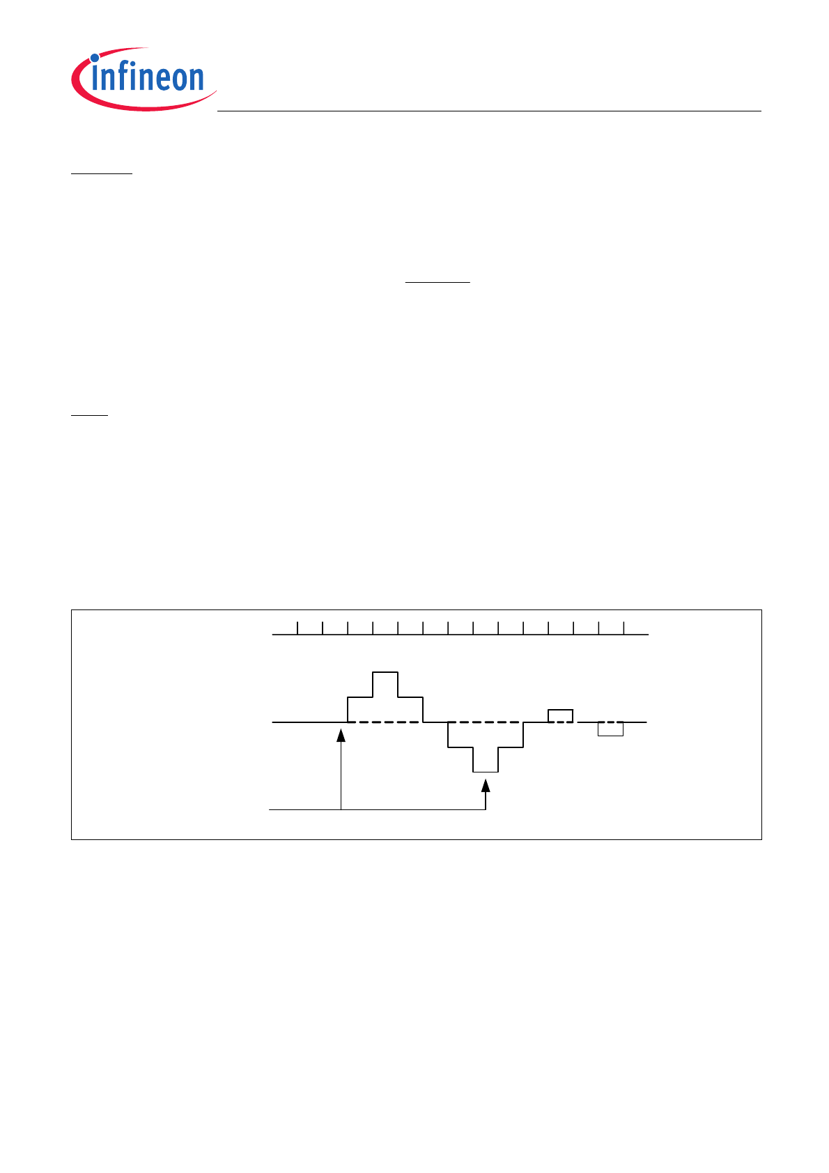
Dither
A triangular dither waveform can be superimposed on the current set point by setting the amplitude and frequency
parameters of the dither waveform via SPI messages #10 and #11. See the SPI message section for details.
The first programmed value is the step size of the dither waveform which is the number of bits added or subtracted
from the setpoint per PWM period. One LSb of the dither step size is 1/4
th
the magnitude of the nominal setpoint
current value. The second programmed value is the number of steps in one quarter of the dither waveform.
When dither is enabled, a new average current set point will not be activated until the current dither cycle has
completed. The dither cycle is completed on the positive zero crossing of the dither waveform. A new dither
amplitude setting or a new dither frequency setting will also not be activated until the current dither cycle has
completed. See
Figure 4
.
Figure 4
New Dither Values Programmed and the Resulting Waveform Timing
Note: The actual measured dither waveform is attenuated and phase shifted according to the frequency response
of the control loop.
CLK
AZ
F
N
M
4
T
∗
∗
=
PWM_START
Dither
Dither
Parameter
Change
TLE8242-2
Block Diagram
Data Sheet
10
Rev. 1.0, 2010-02-09
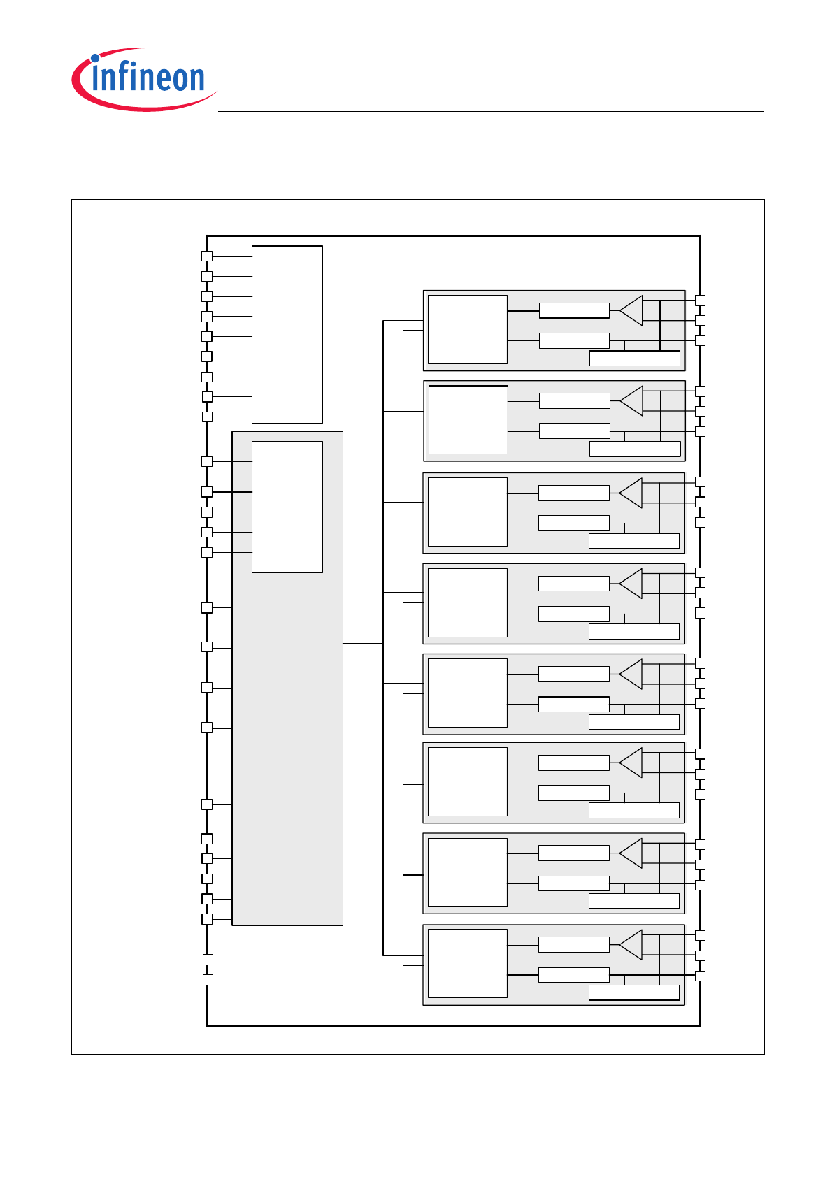
2
Block Diagram
Figure 5
Block Diagram
POS0
OUT0
NEG0
SCK
SI
SO
CS_B
FAULT
RESET_B
PHASE_SYNC
V5D
GND_D
GNDA1
CLK
ENABLE
V_SIGNAL
TEST
Power
POS1
OUT1
NEG1
POS2
OUT2
NEG2
POS3
OUT3
NEG3
POS4
OUT4
NEG4
POS5
OUT5
NEG5
POS6
OUT6
NEG6
POS7
OUT7
NEG7
Logic
SPI
Interface
SO
Supply
BAT
A/D Converter
PWM
Diagnostics
Current Control,
Dither,
PWM,
Autozero,
Channel Logic,
Current Profile
A/D Converter
PWM
Diagnostics
Current Control,
Dither,
PWM,
Autozero,
Channel Logic,
Current Profile
A/D Converter
PWM
Diagnostics
Current Control,
Dither,
PWM,
Autozero,
Channel Logic,
Current Profile
A/D Converter
PWM
Diagnostics
Current Control,
Dither,
PWM,
Autozero,
Channel Logic,
Current Profile
A/D Converter
PWM
Diagnostics
Current Control,
Dither,
PWM,
Autozero,
Channel Logic,
Current Profile
A/D Converter
PWM
Diagnostics
Current Control,
Dither,
PWM,
Autozero,
Channel Logic,
Current Profile
A/D Converter
PWM
Diagnostics
Current Control,
Dither,
PWM,
Autozero,
Channel Logic,
Current Profile
A/D Converter
PWM
Diagnostics
Current Control,
Dither,
PWM,
Autozero,
Channel Logic,
Current Profile
V5A1
V5A2
V5A3
GNDA2
GNDA3
SCI3
SCO2
SCO3
AMUX
GNDSA
GNDSD