

Automotive Power
Data Sheet
Rev. 1.0, 2011-03-23
TLE 8108 EM
Smart 8-Channel Low Side Relay Driver with SPI Interface
coreFLEX TLE8108EM

Data Sheet
2
Rev. 1.0, 2011-03-23
TLE 8108 EM
Smart 8-Channel Low Side Switch
Table of Contents
Table of Contents
1
Overview . . . . . . . . . . . . . . . . . . . . . . . . . . . . . . . . . . . . . . . . . . . . . . . . . . . . . . . . . . . . . . . . . . . . . . . 3
2
Block Diagram . . . . . . . . . . . . . . . . . . . . . . . . . . . . . . . . . . . . . . . . . . . . . . . . . . . . . . . . . . . . . . . . . . . 5
3
Pin Configuration . . . . . . . . . . . . . . . . . . . . . . . . . . . . . . . . . . . . . . . . . . . . . . . . . . . . . . . . . . . . . . . . 6
3.1
Pin Assignment . . . . . . . . . . . . . . . . . . . . . . . . . . . . . . . . . . . . . . . . . . . . . . . . . . . . . . . . . . . . . . . . . . . 6
3.2
Pin Definitions and Functions . . . . . . . . . . . . . . . . . . . . . . . . . . . . . . . . . . . . . . . . . . . . . . . . . . . . . . . . 6
4
General Product Characteristics . . . . . . . . . . . . . . . . . . . . . . . . . . . . . . . . . . . . . . . . . . . . . . . . . . . . 8
4.1
Absolute Maximum Ratings . . . . . . . . . . . . . . . . . . . . . . . . . . . . . . . . . . . . . . . . . . . . . . . . . . . . . . . . . 8
4.2
Thermal Resistance . . . . . . . . . . . . . . . . . . . . . . . . . . . . . . . . . . . . . . . . . . . . . . . . . . . . . . . . . . . . . . . 9
5
Electrical and functional Description of the Device . . . . . . . . . . . . . . . . . . . . . . . . . . . . . . . . . . . 10
5.1
Functional Description of Supply and Input Pins . . . . . . . . . . . . . . . . . . . . . . . . . . . . . . . . . . . . . . . . 10
5.1.1
Power Supply and Reset . . . . . . . . . . . . . . . . . . . . . . . . . . . . . . . . . . . . . . . . . . . . . . . . . . . . . . . . . 10
5.1.2
Switching Inputs IN1 to IN4 . . . . . . . . . . . . . . . . . . . . . . . . . . . . . . . . . . . . . . . . . . . . . . . . . . . . . . . 11
5.2
Power Outputs . . . . . . . . . . . . . . . . . . . . . . . . . . . . . . . . . . . . . . . . . . . . . . . . . . . . . . . . . . . . . . . . . . 12
5.2.1
Inductive Output Clamp . . . . . . . . . . . . . . . . . . . . . . . . . . . . . . . . . . . . . . . . . . . . . . . . . . . . . . . . . . 12
5.2.2
Timing Diagrams . . . . . . . . . . . . . . . . . . . . . . . . . . . . . . . . . . . . . . . . . . . . . . . . . . . . . . . . . . . . . . . 13
5.3
Electrical Characteristics . . . . . . . . . . . . . . . . . . . . . . . . . . . . . . . . . . . . . . . . . . . . . . . . . . . . . . . . . . 14
6
Protection Functions . . . . . . . . . . . . . . . . . . . . . . . . . . . . . . . . . . . . . . . . . . . . . . . . . . . . . . . . . . . . 16
6.1
Overload Protection . . . . . . . . . . . . . . . . . . . . . . . . . . . . . . . . . . . . . . . . . . . . . . . . . . . . . . . . . . . . . . 16
6.2
Overtemperature Protection . . . . . . . . . . . . . . . . . . . . . . . . . . . . . . . . . . . . . . . . . . . . . . . . . . . . . . . . 16
6.3
Reverse Polarity Protection . . . . . . . . . . . . . . . . . . . . . . . . . . . . . . . . . . . . . . . . . . . . . . . . . . . . . . . . 16
6.4
Protection Characteristics . . . . . . . . . . . . . . . . . . . . . . . . . . . . . . . . . . . . . . . . . . . . . . . . . . . . . . . . . . 17
7
Diagnosis Features . . . . . . . . . . . . . . . . . . . . . . . . . . . . . . . . . . . . . . . . . . . . . . . . . . . . . . . . . . . . . . 18
7.1
Diagnosis Characteristics . . . . . . . . . . . . . . . . . . . . . . . . . . . . . . . . . . . . . . . . . . . . . . . . . . . . . . . . . . 19
8
Serial Peripheral Interface (SPI) . . . . . . . . . . . . . . . . . . . . . . . . . . . . . . . . . . . . . . . . . . . . . . . . . . . 21
8.1
SPI Signal Description . . . . . . . . . . . . . . . . . . . . . . . . . . . . . . . . . . . . . . . . . . . . . . . . . . . . . . . . . . . . 21
8.2
Daisy Chain Capability . . . . . . . . . . . . . . . . . . . . . . . . . . . . . . . . . . . . . . . . . . . . . . . . . . . . . . . . . . . . 23
8.3
SPI Protocol . . . . . . . . . . . . . . . . . . . . . . . . . . . . . . . . . . . . . . . . . . . . . . . . . . . . . . . . . . . . . . . . . . . . 24
8.3.1
Timing Diagrams . . . . . . . . . . . . . . . . . . . . . . . . . . . . . . . . . . . . . . . . . . . . . . . . . . . . . . . . . . . . . . . 25
8.4
SPI Characteristics . . . . . . . . . . . . . . . . . . . . . . . . . . . . . . . . . . . . . . . . . . . . . . . . . . . . . . . . . . . . . . . 25
9
Application Information . . . . . . . . . . . . . . . . . . . . . . . . . . . . . . . . . . . . . . . . . . . . . . . . . . . . . . . . . . 27
10
Package Outlines . . . . . . . . . . . . . . . . . . . . . . . . . . . . . . . . . . . . . . . . . . . . . . . . . . . . . . . . . . . . . . . 28
11
Revision History . . . . . . . . . . . . . . . . . . . . . . . . . . . . . . . . . . . . . . . . . . . . . . . . . . . . . . . . . . . . . . . . 29
PG-SSOP-24
Type
Package
Marking
TLE8108EM
PG-SSOP-24
Data Sheet
3
Rev. 1.0, 2011-03-23
Smart 8-Channel Low Side Relay Driver with SPI Interface
coreFLEX
TLE8108EM
1
Overview
Features
•
4 input pins providing flexible PWM configuration
•
Active Clamping
•
Low Power Consumption Mode (Standby)
•
16 bit SPI for diagnostics and control
•
Daisy chain capability also compatible with 8bit SPI devices
•
Green product (RoHS compliant)
•
AEC qualified
Description
The TLE8108EM is an 8-Channel Low Side Switch in PG-SSOP-24 package providing embedded protective
functions.
It is especially designed as relay driver for powertrain automotive applications.
A serial peripheral interface (SPI) is implemented for control and diagnosis of the device and the load.
Four configurable direct inputs are available to control the outputs in PWM.
The device is monolithically integrated. The internal switches are power n-MOSFETs.
Table 1
Basic Electrical Data
Supply voltage
V
DD
4.5V ... 5.5V
Max. ON State resistance at
T
j
= 150°C for each channel
R
DS(ON,max)
1.7
Ω
Continuos load current
I
L (cont)
400mA
Overload switch off threshold
I
D (OVL,min)
500mA
Output leakage current per channel
I
D (STB,max)
5µA
Minimal drain to source clamping voltage
V
DS(CL)
41V
Maximum SPI clock frequency
f
SCLK,max
5MHz

Data Sheet
4
Rev. 1.0, 2011-03-23
TLE 8108 EM
Smart 8-Channel Low Side Switch
Overview
Diagnostic Feedback Information
•
Latched diagnostic information via SPI register
•
Overtemperature detection (DOT)
•
Overload detection corresponding Short Circuit to Battery (SCB) in ON state.
•
Open load detection in OFF state (OL)
•
Short Circuit to GND detection in OFF state (SCG)
Protection Functions
•
Overload switch off
•
Overtemperature switch off
•
Electrostatic discharge (ESD)
Application
•
Resistive, inductive and capacitive loads
•
Especially designed for driving relays in automotive applications
General Information
The TLE8108EM is an 8-Channel Low Side Relay Switch designed for typical automotive relays, providing
embedded protective functions. The PG-SSOP-24 package is used to get a footprint optimized solution. The 16 bit
serial peripheral interface (SPI) is utilized for control and diagnosis of the device and the loads. The SPI interface
provides daisy chain capability.
The TLE8108EM is equipped with 4 input pins that can be used to directly control their dedicated channels thus
offering flexibility in design and PCB layout. The input multiplexer is controlled via SPI.
The device provides full diagnosis of the load, which is open load, short circuit to ground, as well as a short circuit
to battery detection. The SPI diagnosis bits indicate latched fault conditions that may have occurred.
Each output stage is protected against short circuit. In case of Overload, the affected channel switches off. There
are temperature sensors for each channel to protect the device in case of Overtemperature.
The device is supplied by a single power supply. It is operating at 5V nominal value.
The internal switches are power n-MOSFETs. The inputs are ground referenced CMOS compatible. The device
is monolithically integrated in Smart Power Technology.
All output pins are available at one side of the device while the other side bundles the signals to the microcontroller,
thus facilitating the PCB layout.
It is possible to set each channel in a Clear Mode (CLR) in order to clear Diagnosis flags; in CLR state output is
switched off and diagnosis currents are disabled.
A Standby mode of the Device (STB) can be entered if all the channels are set into CLR state; in STB mode the
power consumpiton is reduced to the minimum.
TLE 8108 EM
Smart 8-Channel Low Side Switch
Block Diagram
Data Sheet
5
Rev. 1.0, 2011-03-23
2
Block Diagram
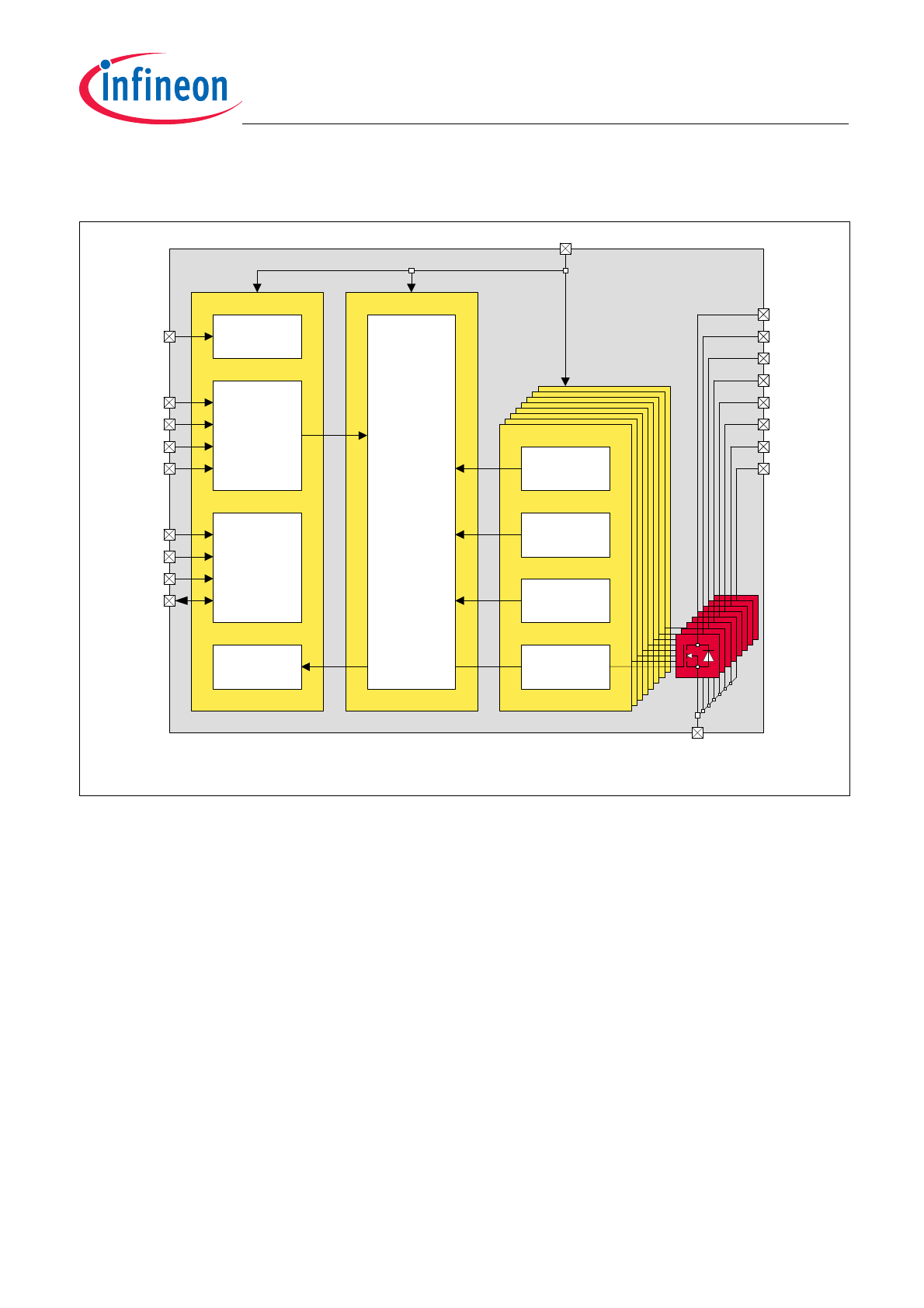
Figure 1
Block Diagram for the TLE8108EM
Block Diagram.vsd
Standby
Control
Control,
Diagnostic,
Protection
Functions
Input MUX,
Control
SPI
Diagnosis
Register
IN1
IN2
IN3
IN4
Gate Control
Short Circuit
Detection
Temperature
Sensor
Open Load
Detection
CS
SCLK
SI
SO
RST
VDD
GND
OUT1
OUT2
OUT3
OUT4
OUT5
OUT6
OUT7
OUT8
Data Sheet
6
Rev. 1.0, 2011-03-23
TLE 8108 EM
Smart 8-Channel Low Side Switch
Pin Configuration
3
Pin Configuration
3.1
Pin Assignment
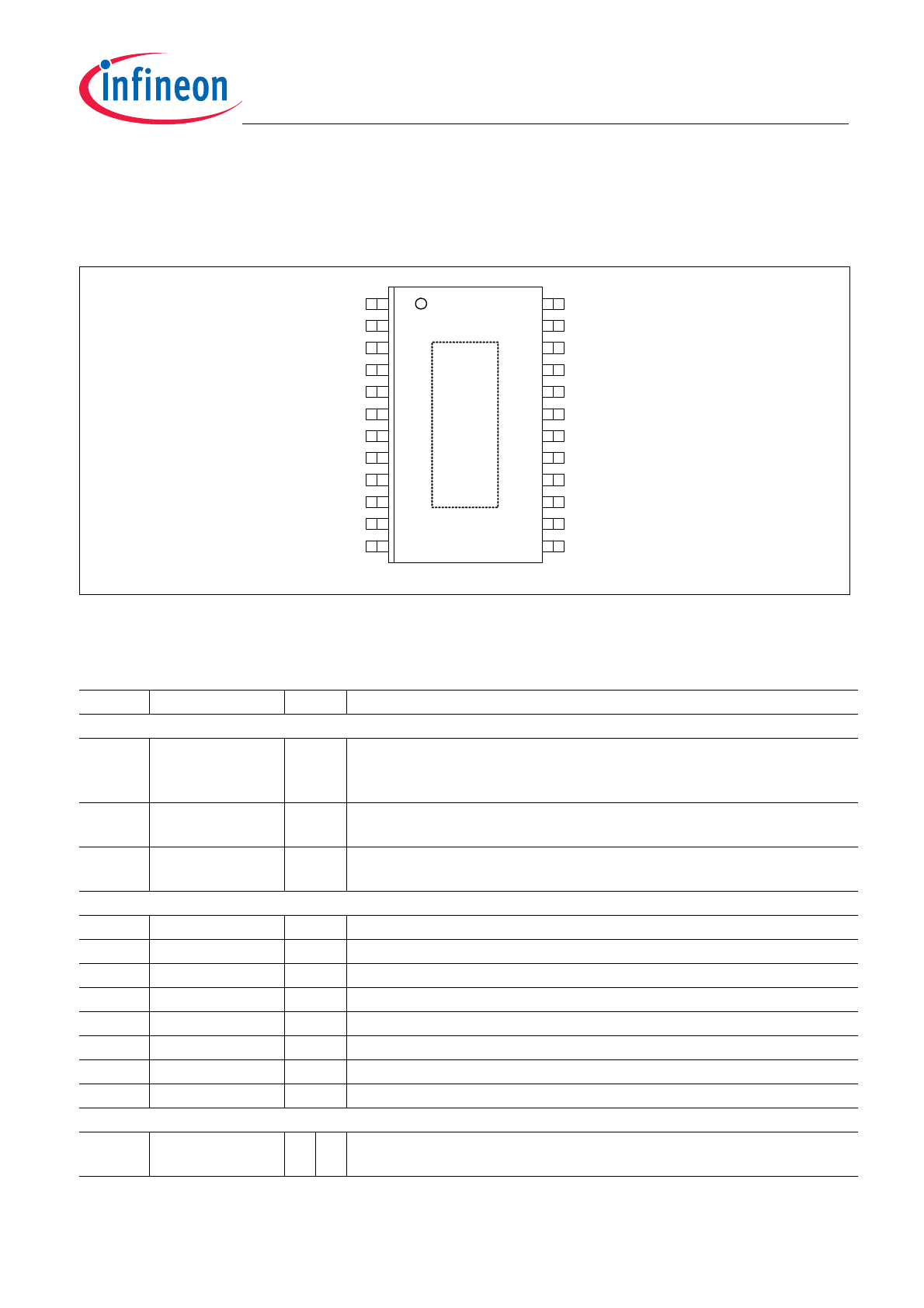
Figure 2
Pin Configuration
3.2
Pin Definitions and Functions
Pin
Symbol
I/O
1)
Function
Power Supply
13,24
VDD
-
Supply voltage; Connected to 5V voltage with reverse protection diode
and filter against EMC; Both pins must be connected to the supply without
parasitic resistors
1,2,11,12 GND
-
Ground; common ground for digital, analog and power; Pins must be
connected together without parasitic resistors
Cooling
TAB
GND
-
Cooling TAB (bottom side); Internally connected to ground; Pin must be
connected externally to ground without parasitic resistors
Power Stages
3
OUT1
O
Output channel 1; Drain of power transistor channel 1
4
OUT2
O
Output channel 2; Drain of power transistor channel 2
5
OUT3
O
Output channel 3; Drain of power transistor channel 3
6
OUT4
O
Output channel 4; Drain of power transistor channel 4
7
OUT5
O
Output channel 5; Drain of power transistor channel 5
8
OUT6
O
Output channel 6; Drain of power transistor channel 6
9
OUT7
O
Output channel 7; Drain of power transistor channel 7
10
OUT8
O
Output channel 8; Drain of power transistor channel 8
Inputs
17
IN1
I
PD Active Low; Control input; Digital input 3.3V or 5V; If not used, pin must be
connected to GND
Pin Configuration.vsd
Cooling
TAB
GND
1
2
3
4
5
6
7
8
9
10
11
12
GND
OUT1
OUT2
OUT3
OUT4
OUT5
OUT6
OUT7
OUT8
GND
GND
24
23
22
21
20
19
18
17
16
15
14
13
VDD
CS
SI
RST
SCLK
SO
N.U.
IN1
IN2
IN3
IN4
VDD
TOP VIEW
TLE 8108 EM
Smart 8-Channel Low Side Switch
Pin Configuration
Data Sheet
7
Rev. 1.0, 2011-03-23
16
IN2
I
PD Active Low; Control input; Digital input 3.3V or 5V; If not used, pin must be
connected to GND
15
IN3
I
PD Active Low; Control input; Digital input 3.3V or 5V; If not used, pin must be
connected to GND
14
IN4
I
PD Active Low; Control input; Digital input 3.3V or 5V; If not used, pin must be
connected to GND
18
N.C.
I
PD Not Connected; pin must be tied to GND
21
RST
I
PD Active Low; Reset input pin; Digital input 3.3V or 5V
SPI
23
CS
I
PU Active Low; SPI chip select; Digital input 3.3V or 5V
20
SCLK
I
PD Active Low; Serial clock; Digital input 3.3V or 5V
22
SI
I
PD Active Low; Serial data in; Digital input 3.3V or 5V.
19
SO
O
2)
Serial data out; Digital output with voltage level referring to VDD
1) O=Output;
I=Input;
PD=integrated pull-down resistor;
PU=integrated pull-up resistor
2) SO is set to tristate if SPI is inactive (CS is high or
RST
is low)
Pin
Symbol
I/O
1)
Function
Data Sheet
8
Rev. 1.0, 2011-03-23
TLE 8108 EM
Smart 8-Channel Low Side Switch
General Product Characteristics
4
General Product Characteristics
4.1
Absolute Maximum Ratings
Note: Stress above the ones listed here may cause permanent damage to the device. Exposure to absolute
maximum rating conditions for extended periods may affect device reliability.
Note: Integrated protection functions are designed to prevent IC destruction under fault conditions described in the
data sheet. Fault conditions are considered as “outside” normal operating range. Protection functions are
not designed for continuous repetitive operation.
Absolute Maximum Ratings
1)
Unless otherwise specified:
T
j
= -40°C to +150°C;
V
DD
= 4.5V to 5.5V
All voltages with respect to ground, positive current flowing into pin
1) Not subject to production test, specified by design.
Pos.
Parameter
Symbol
Limit Values
Unit
Conditions
Min.
Max.
Power Supply
4.1.1
Supply voltage
V
DD
-0.3
5.5
V
-
4.1.2
Output voltage for short circuit protection
(single pulse)
V
DS_SC
0
36
V
-
Power Stages
4.1.3
Load current
I
D
-0.5
0.5
A
-
4.1.4
Voltage at power transistor
V
DS
-0.3
41
V
Active Clamped
Clamping Energy - Singel Pulse
2)
2) Triangular Pulse Shape (Inductance Discharge):
I
D
(t) =
I
D
(0)
×
(1 -
t
/
t
pulse
); 0 <
t
<
t
pulse
.
4.1.5
Single Clamping Energy
per Channel
E
AS
-
20
mJ
I
D
= 0.18A
1 Single Pulse
Logic Pins
4.1.6
IN1 to IN4; Voltage at input pins
V
IN
-0.3
V
DD
+ 0.3 V
3)
4.1.7
RST; Voltage at reset pin
V
RST
-0.3
V
DD
+ 0.3 V
3)
4.1.8
CS; Voltage at chip select
V
CS
-0.3
V
DD
+ 0.3 V
3)
3) Level must not exceed
V
DD
+0.3V < 5.5V
4.1.9
SCLK; Voltage at serial clock pin
V
SCLK
-0.3
V
DD
+ 0.3 V
3)
4.1.10
SI; Voltage at serial input pin
V
SI
-0.3
V
DD
+ 0.3 V
3)
4.1.11
SO; Voltage at serial output pin
V
SO
-0.3
V
DD
+ 0.3 V
3)
Temperatures
4.1.12
Junction Temperature
T
j
-40
150
°C
-
4.1.13
Junction Temperature
T
j
-40
165
°C
Dynamic
Conditions,
100h max total
4.1.14
Storage Temperature
T
stg
-55
150
°C
-
ESD Susceptibility
4.1.15
ESD Resistivity
V
ESD
-4
4
kV
HBM
4)
4) ESD susceptibility, HBM according to EIA/JESD 22-A114-F
TLE 8108 EM
Smart 8-Channel Low Side Switch
General Product Characteristics
Data Sheet
9
Rev. 1.0, 2011-03-23
4.2
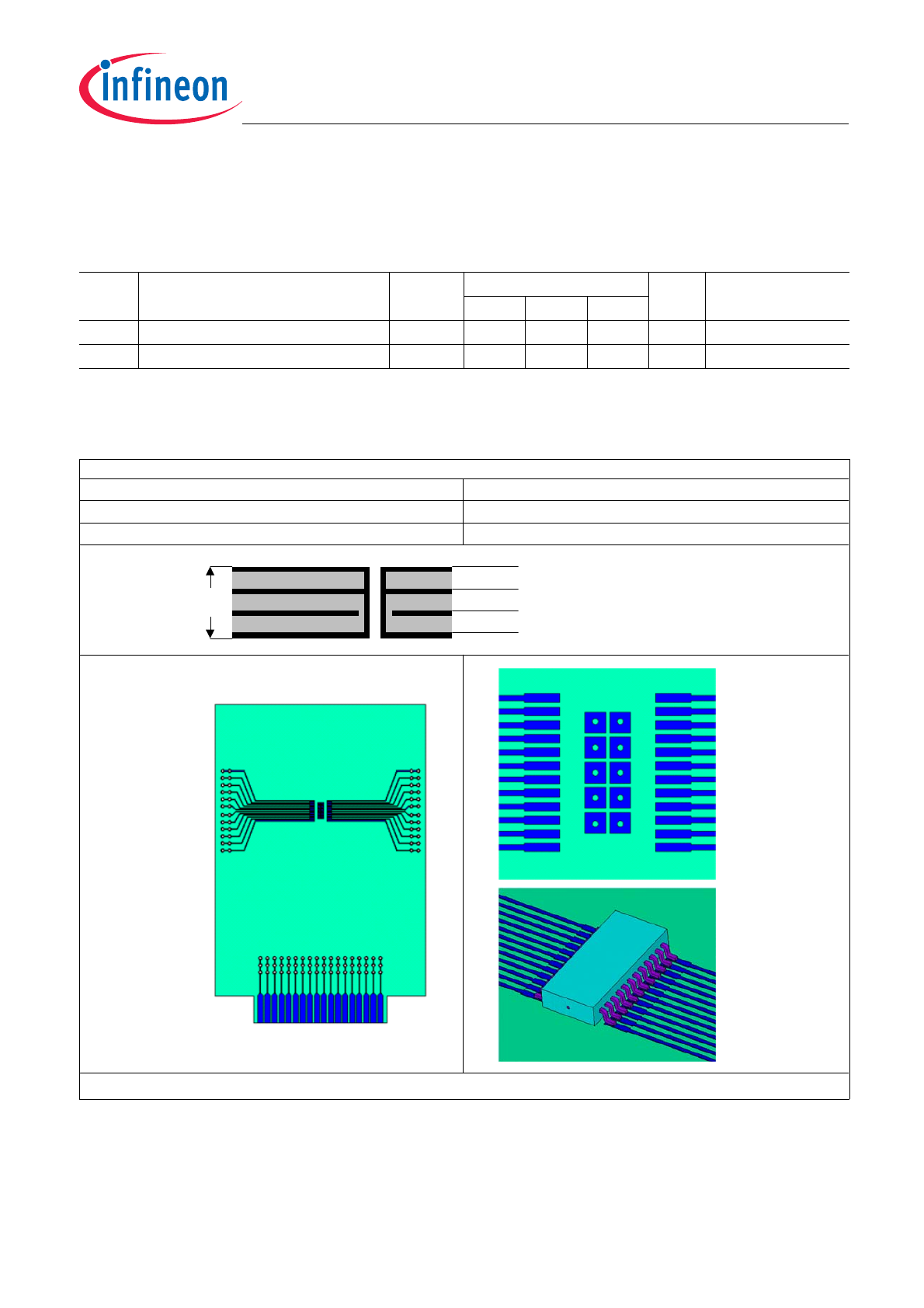
Thermal Resistance
Note: This thermal data was generated in accordance with JEDEC JESD51 standards.
For more information go to
www.jedec.org
.
Figure 3
PG-SSOP-24 PCB setup
Pos.
Parameter
Symbol
Limit Values
Unit
Conditions
Min.
Typ.
Max.
4.2.1
Junction to Case
R
thJC
-
-
7
K/W
P
TOT
= 1W
1)
2)
3)
1) Not subject to production test, specified by design.
2) Homogenous power distrubution over all channels (all power stages equally heated), dependent on cooling setup.
3) Refer to
Figure 3
for the setup.
4.2.2
Junction to Ambient (2s2p)
R
thJA
-
40
-
K/W
P
TOT
= 1W
1)
2)
3)
Rth PCB setup.vsd
1.5
m
m
35µm, 90% metallization
70µm modeled (traces)
35µm, 90% metallization
70µm, 5% metallization
Metallization:
Dimensions:
Thermal Vias:
76.2 x 114.3 x 1.5 mm³ , FR4
JEDEC 2s2p (JESD 51-7) + (JESD 51-5)
F =0.3mm; plating 25µm; 10 pcs. for PG-SSOP-24
Data Sheet
10
Rev. 1.0, 2011-03-23
TLE 8108 EM
Smart 8-Channel Low Side Switch
Electrical and functional Description of the Device
5
Electrical and functional Description of the Device
The TLE8108EM is a 8-Channel Low Side Relay Switch.
The power stages are composed of n-MOSFET transistors.
5.1
Functional Description of Supply and Input Pins
5.1.1
Power Supply and Reset
The TLE8108EM is supplied by a single power supply line
V
DD
with two input pins which must be connected
together. After power supply start-up, the input registers of the device are programmed to OFF mode for all
channels. The output registers must be reset to their default values by programming the Clear mode for all
channels once.
Capacitors at the supply pins
V
DD
to GND are recommended.
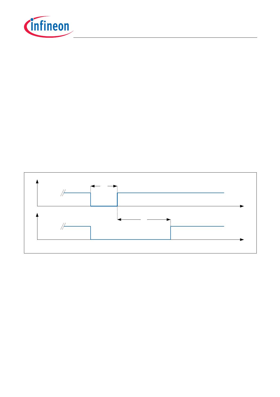
There is a reset pin available. Low level at this pin causes all registers to be set to their default values and the
quiescent supply currents are minimized. This is also true for the Standby Mode in case all channels are
programmed to Clear.
Figure 4
shows the timing requirements for the RST pin to be enabled and for the device
to wake up.
Figure 4
Reset Timings
Reset Timing.vsd
READY
NOT READY
READY
t
RST
t
WU
RST
DEVICE
STATUS
t
t