

TLE7242-2G
4 Channel Fixed Frequency Constant Current
Control IC
Data Sheet, Rev. 1.1, May 2011
Automotive Power

Data Sheet
2
Rev. 1.1, 2011-05-27
TLE7242-2G
Table of Contents
Table of Contents . . . . . . . . . . . . . . . . . . . . . . . . . . . . . . . . . . . . . . . . . . . . . . . . . . . . . . . . . . . . . . . . 2
1
Overview . . . . . . . . . . . . . . . . . . . . . . . . . . . . . . . . . . . . . . . . . . . . . . . . . . . . . . . . . . . . . . . . . . . . . . . 3
1.1
Features . . . . . . . . . . . . . . . . . . . . . . . . . . . . . . . . . . . . . . . . . . . . . . . . . . . . . . . . . . . . . . . . . . . . . . . . 3
1.2
Applications . . . . . . . . . . . . . . . . . . . . . . . . . . . . . . . . . . . . . . . . . . . . . . . . . . . . . . . . . . . . . . . . . . . . . 4
1.3
General Description . . . . . . . . . . . . . . . . . . . . . . . . . . . . . . . . . . . . . . . . . . . . . . . . . . . . . . . . . . . . . . . 4
1.3.1
On / Off Mode Operation . . . . . . . . . . . . . . . . . . . . . . . . . . . . . . . . . . . . . . . . . . . . . . . . . . . . . . . . . . 4
1.3.2
Constant Current Mode Operation . . . . . . . . . . . . . . . . . . . . . . . . . . . . . . . . . . . . . . . . . . . . . . . . . . . 5
2
Block Diagram . . . . . . . . . . . . . . . . . . . . . . . . . . . . . . . . . . . . . . . . . . . . . . . . . . . . . . . . . . . . . . . . . . . 9
3
Pin Configuration . . . . . . . . . . . . . . . . . . . . . . . . . . . . . . . . . . . . . . . . . . . . . . . . . . . . . . . . . . . . . . . 10
3.1
Pin Assignment . . . . . . . . . . . . . . . . . . . . . . . . . . . . . . . . . . . . . . . . . . . . . . . . . . . . . . . . . . . . . . . . . 10
3.2
Pin Definitions and Functions . . . . . . . . . . . . . . . . . . . . . . . . . . . . . . . . . . . . . . . . . . . . . . . . . . . . . 10
4
General Product Characteristics . . . . . . . . . . . . . . . . . . . . . . . . . . . . . . . . . . . . . . . . . . . . . . . . . . . 12
4.1
Maximum Ratings . . . . . . . . . . . . . . . . . . . . . . . . . . . . . . . . . . . . . . . . . . . . . . . . . . . . . . . . . . . . . . . . 12
4.2
Functional Range . . . . . . . . . . . . . . . . . . . . . . . . . . . . . . . . . . . . . . . . . . . . . . . . . . . . . . . . . . . . . . . . 13
4.3
Thermal Resistance . . . . . . . . . . . . . . . . . . . . . . . . . . . . . . . . . . . . . . . . . . . . . . . . . . . . . . . . . . . . . . 13
5
Functional Description and Electrical Characteristics . . . . . . . . . . . . . . . . . . . . . . . . . . . . . . . . . 14
5.1
Supply and Reference . . . . . . . . . . . . . . . . . . . . . . . . . . . . . . . . . . . . . . . . . . . . . . . . . . . . . . . . . . . . 14
5.2
Input / Output . . . . . . . . . . . . . . . . . . . . . . . . . . . . . . . . . . . . . . . . . . . . . . . . . . . . . . . . . . . . . . . . . . . 15
5.3
Diagnostics . . . . . . . . . . . . . . . . . . . . . . . . . . . . . . . . . . . . . . . . . . . . . . . . . . . . . . . . . . . . . . . . . . . . . 16
5.3.1
On-State Diagnostics . . . . . . . . . . . . . . . . . . . . . . . . . . . . . . . . . . . . . . . . . . . . . . . . . . . . . . . . . . . . 19
5.3.2
Off-State Diagnostics . . . . . . . . . . . . . . . . . . . . . . . . . . . . . . . . . . . . . . . . . . . . . . . . . . . . . . . . . . . . 20
5.4
Output Driver . . . . . . . . . . . . . . . . . . . . . . . . . . . . . . . . . . . . . . . . . . . . . . . . . . . . . . . . . . . . . . . . . . . 24
5.5
Current Control . . . . . . . . . . . . . . . . . . . . . . . . . . . . . . . . . . . . . . . . . . . . . . . . . . . . . . . . . . . . . . . . . . 24
5.6
Serial Peripheral Interface (SPI) . . . . . . . . . . . . . . . . . . . . . . . . . . . . . . . . . . . . . . . . . . . . . . . . . . . . . 25
5.6.1
SPI Signal Description . . . . . . . . . . . . . . . . . . . . . . . . . . . . . . . . . . . . . . . . . . . . . . . . . . . . . . . . . . . 26
5.6.2
SPI Message Structure . . . . . . . . . . . . . . . . . . . . . . . . . . . . . . . . . . . . . . . . . . . . . . . . . . . . . . . . . . 28
5.6.2.1
SPI Message #0 - IC Version / Manufacturer . . . . . . . . . . . . . . . . . . . . . . . . . . . . . . . . . . . . . . . 28
5.6.2.2
SPI Message #1 - Main Period Set . . . . . . . . . . . . . . . . . . . . . . . . . . . . . . . . . . . . . . . . . . . . . . . 29
5.6.2.3
SPI Message #2 - PWM Offset . . . . . . . . . . . . . . . . . . . . . . . . . . . . . . . . . . . . . . . . . . . . . . . . . . 30
5.6.2.4
SPI Message #3 - Current Set Point and Dither Amplitude Set . . . . . . . . . . . . . . . . . . . . . . . . . . 31
5.6.2.5
SPI Message #4 - Dither Period Set . . . . . . . . . . . . . . . . . . . . . . . . . . . . . . . . . . . . . . . . . . . . . . 33
5.6.2.6
SPI Message #5 - Control Variable Set (KP and KI) . . . . . . . . . . . . . . . . . . . . . . . . . . . . . . . . . . 34
5.6.2.7
SPI Message #6 - Dynamic Threshold Value Set . . . . . . . . . . . . . . . . . . . . . . . . . . . . . . . . . . . . 36
5.6.2.8
SPI Message #7 - On/Off Control and Fault Mask Configuration . . . . . . . . . . . . . . . . . . . . . . . . 38
5.6.2.9
SPI Message #8 - Diagnostic Configuration . . . . . . . . . . . . . . . . . . . . . . . . . . . . . . . . . . . . . . . . 40
5.6.2.10
SPI Message #9 - Diagnostic Read . . . . . . . . . . . . . . . . . . . . . . . . . . . . . . . . . . . . . . . . . . . . . . . 42
5.6.2.11
SPI Message #10 - Current Read . . . . . . . . . . . . . . . . . . . . . . . . . . . . . . . . . . . . . . . . . . . . . . . . 43
5.6.2.12
SPI Message #11 - Autozero Read . . . . . . . . . . . . . . . . . . . . . . . . . . . . . . . . . . . . . . . . . . . . . . . 44
5.6.2.13
SPI Message #12 - Duty Cycle Read . . . . . . . . . . . . . . . . . . . . . . . . . . . . . . . . . . . . . . . . . . . . . 46
6
Application Information . . . . . . . . . . . . . . . . . . . . . . . . . . . . . . . . . . . . . . . . . . . . . . . . . . . . . . . . . . 47
6.1
Further Application Information . . . . . . . . . . . . . . . . . . . . . . . . . . . . . . . . . . . . . . . . . . . . . . . . . . . . . . 47
7
Package Outlines . . . . . . . . . . . . . . . . . . . . . . . . . . . . . . . . . . . . . . . . . . . . . . . . . . . . . . . . . . . . . . . 48
8
Revision History . . . . . . . . . . . . . . . . . . . . . . . . . . . . . . . . . . . . . . . . . . . . . . . . . . . . . . . . . . . . . . . . 49
Table of Contents
PG-DSO-28
Type
Package
Marking
TLE7242-2G
PG-DSO-28
TLE7242-2G
Data Sheet
3
Rev. 1.1, 2011-05-27
4 Channel Fixed Frequency Constant Current Control
IC
TLE7242-2G
1
Overview
1.1
Features
•
Low side constant current control pre-driver integrated circuit
•
Four independent channels
•
Output current programmable with 11 bit resolution
– Current range = 0 to 1.2A (typ) with a 0.2
sense resistor
– Resolution = 0.78125 mA/bit (typ) with a 0.2
sense resistor
– +/- 2% full scale error over temperature when autozero is used
•
Programmable PWM frequency via SPI from approximately
50 Hz to 4 KHz (typ)
•
Programmable KP and KI coefficients for the PI controller for each
channel
•
Programmable Transient Mode of operation to reduce settling time when large changes in the current set point
are commanded.
•
Programmable superimposed dither.
– Dither programmed by setting a dither step size and the number of PWM periods in each dither period
– Programmed via the SPI interface
– The dither for each channel can be enabled and programmed independently
•
Programmable synchronization of the PWM control signals.
– Phase delay time set via the SPI interface
– Synchronization initiated via signal at the PHASE_SYNC input pin.
– Channels within one device and between multiple devices can be synchronized.
•
Each channel can be configured to function as a simple on/off predriver or a constant current predriver via SPI
•
Interface and Control
– 32 Bit SPI (Serial Peripheral Interface) - Slave only
– ENABLE pin to disable all channels or freeze all channels
– Active low RESET_B pin resets internal registers to their default state and disables all channels.
– Open drain FAULT pin can be programmed to transition low when various faults are detected.
– 5.0V and 3.3V logic compatible I/O
•
Protection
– Over current shutdown - monitored at POSx pin.
– Programmable over current threshold
– Programmable over current delay time
– Programmable over current retry time
– Battery pin (BAT) overvoltage shutdown.
•
Diagnostics
– Over current

TLE7242-2G
Overview
Data Sheet
4
Rev. 1.1, 2011-05-27
– Open load in on state
– Open load in off state
– Short to ground
– Test complete bit - indicates that fault detection test has completed
•
Control loop monitor capabilities
– The average current measurement over the last completed PWM cycle of each channel can be accessed
via SPI.
– The PWM duty cycle of each channel can be accessed via SPI
– The auto zero values used to null the offsets of the input amplifiers can be accessed via SPI
•
Required External Components:
– N-Channel Logic level (5V) MOSFET transistor with typical Ron
100 m (e.g. BSO604NS2)
– Recirculation diode (ultrafast)
– Sense resistor (0.2
for 1.2A average output current range)
•
Green Product (RoHS compliant)
•
AEC Qualified
1.2
Applications
•
Variable Force Solenoids (e.g. automatic transmission solenoids)
•
Other constant current solenoids
– Idle Air Control
– Exhaust Gas Recirculation
– Vapor Management Valve
– Suspension Control
1.3
General Description
The TLE7242 2G IC is a four channel low-side constant current control predriver IC. Each channel can be
configured to function either in on/off mode or in constant current mode by setting the appropriate MODE bit in SPI
message #7.
1.3.1
On / Off Mode Operation
For On/Off operation, the POSx and NEGx pins must be connected to the circuit in either of the configurations
shown in
Figure 1
. If the sense resistor is included, the load current can be monitored by the microcontroller via
a SPI command. The open load in on state fault detection feature is disabled in on/off mode.
Note: An external flyback clamp is required in this configuration otherwise the IC may be damaged.
Data Sheet
5
Rev. 1.1, 2011-05-27
TLE7242-2G
Overview
Figure 1
External Circuit Diagram for On/Off Mode Operation
1.3.2
Constant Current Mode Operation
During constant current operation, the POSx and NEGx pins must be connected to the circuit in the configuration
shown in
Figure 2
.
Note: An external recirculation diode is required in this configuration otherwise the IC may be damaged.
Figure 2
External Circuit Diagram for Constant Current Mode Operation
The constant current control circuit can operate in two modes; steady state mode and transient mode.
Steady-State Mode
During steady-state operation, the PWM control signal driven at the OUTx pin is controlled by the control loop
shown in
Figure 3
. The PWM Frequency is programmed via the SPI message # 1. In this message the main period
divider, N, can be set to any value between 79 and 2
14
-1. The equation for calculating the PWM frequency is:
Solenoid
R
SENSE
POSx
NEGx
OUTx
POSx
NEGx
OUTx
R
G
R
G
Q
DRV
Q
DRV
Solenoid
C
ESD
C
ESD
V
BAT
V
BAT
POSx
NEGx
OUTx
Solenoid
R
SENSE
D
RECIRC
Q
DRV
C
ESD
V
BAT
R
G
N
F
F
CLK
PWM
*
32
TLE7242-2G
Overview
Data Sheet
6
Rev. 1.1, 2011-05-27
The 11 bit Current Set Point is programmed via the SPI message #3. The equation for calculating the current
setpoint is:
The Proportional coefficient (KP) and the Integral coefficient (KI) of the control loop are programmed in SPI
message #5. The KP and KI values should be set to values that result in the desired transient response of the
control loop. The duty cycle of the OUTx pin can be calculated from the difference equations:
where error is the difference between the commanded average current and measured average current in units of
Amps.
where k indicates the integral number of PWM periods that have elapsed since current regulation was initiated.
Figure 3
Control Loop - Steady-State Mode
Auto Zero
When a channel is configured for constant current operation and the current set point is 000h for 256 consecutive
PWM periods, an autozero sequence is initiated. The autozero sequence will measure the offset of the current
SENSE
setpoint
R
(11bit)
t
setpoin
mA
Current
320
2
]
[
11
)
1
(
1
*
28
.
1
)
(
)
(
1
*
28
.
1
k
INT
k
error
N
Rsense
KI
k
INT
k
INT
k
error
N
Rsense
KP
k
DutyCycle
A/D
Average
Autozero
Value
“ON”
-
CURRENT SET
POINT
DITHER STEP SIZE
Dither
Generation
+
+
+
KP
KI
PWM
Block
PWM
CLK
+
+
DITHER STEPS
OUTx
POSx
NEGx
Amp
+
-
Auto Zero
Autozero
Value
“OFF”
DUTY
CYCLE
CURRENT
READ
PRE-
LOAD
Italics = CAN BE MONITORED VIA SPI
Underlined = CAN BE PROGRAMMED VIA SPI
Data Sheet
7
Rev. 1.1, 2011-05-27
TLE7242-2G
Overview
measurement amplifiers. If the autozero function is enabled in SPI message #7, then the measured offset will be
subtracted from the A/D converter output as shown in
Figure 3
when the current set point is greater than 0.
Dither
A triangular dither waveform can be superimposed on the current set point by setting the Dither Enable bit in SPI
message #3. The amplitude and frequency of the dither waveform are programmed for each channel via SPI
messages #3 and #4. See the SPI message section for details.
The first programmed value is the step size of the dither waveform which is the number of bits added or subtracted
from the setpoint per PWM period. One LSb of the dither step size is 1/16 the magnitude of the nominal setpoint
current value. The second programmed value is the number of steps in one quarter of the dither waveform.
When dither is enabled, a new dither amplitude setting, a new dither frequency setting, or a dither disable
command will not be activated until the current dither cycle has completed - see
Figure 4
. The dither cycle is
completed on the positive zero crossing of the dither waveform. A change in the setpoint current, however, is
activated at the start of the next PWM period.
Figure 4
New Dither Values Programmed and the Resultant Waveform Timing
Note: the actual dither waveform is attenuated and phase shifted according to the frequency response of the
control loop.
If a channel enters transient mode operation while the dither waveform is active, the dither wave-form will pause
until transient mode is exited.
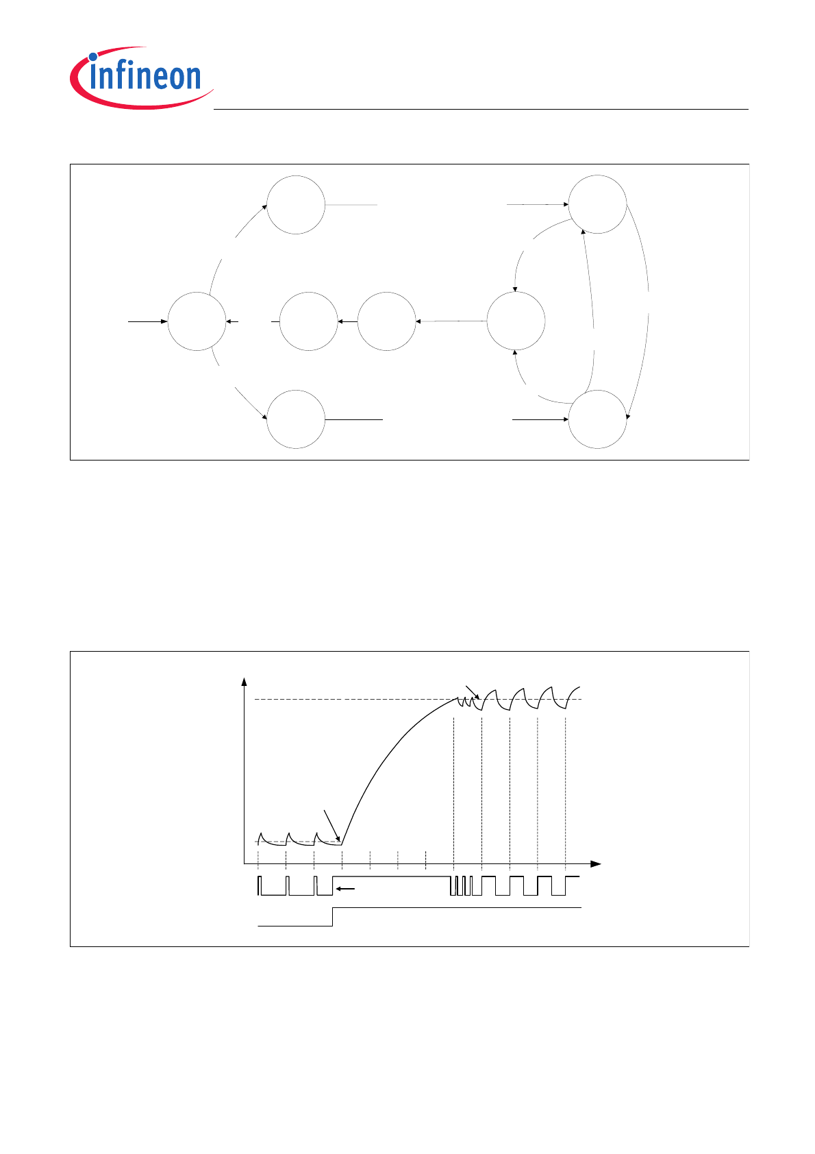
Transient Mode
When a large change in the current set point occurs, the device can be programmed to enter transient mode of
operation. The setpoint change threshold required to initiate transient mode can be programmed in
SPI message #6. The purpose of this mode of operation is to reduce the transition time of the load current after a
large change in setpoint. In this mode of operation the OUTx pin signal is controlled by the state machine shown
in
Figure 5
. The control method in this mode is similar to hysteretic control, the OUTx signal transitions high or
low based on the immediate value of the measured output current. The PWM frequency is not fixed in this mode
of operation. The device will automatically switch from transient mode of operation to steady state operation at the
start of the first PWM period after the new set point has been reached.
PWM_START
Dither
Dither
Parameter
Change
TLE7242-2G
Overview
Data Sheet
8
Rev. 1.1, 2011-05-27
Figure 5
Transient Mode State Diagram
A typical current waveform during transient mode operation is shown in
Figure 6
. Starting from a set point I, the
new set point II is accepted a short time after the rising edge on CS_B. The OUTx pin remains high until the
measured load current has reached the new set point. The OUTx pin is then toggled on and off to maintain the
load current near the new set point until the next PWM period begins. The device will then switch back to steady
state control and the OUTx pin will be controlled by the control loop shown in
Figure 3
.
During the transition from transient mode operation to steady state operation, the integrator is pre-loaded with a
SPI programmable value. This value should be chosen to give an initial PWM duty cycle approximately equal to
the duty cycle required to regulate the load current at the new set point.
Figure 6
Transient Mode Timing Diagram
Steady-
State
Mode
Reset
OUTx = High
OUTx = Low
OUTx = High
LEAVE
HYST MODE
OUTx := LOW
Controller := stop
CALC
DC
OUTx := LOW
Controller := stop
Set Point change > Threshold
New Set Point > Old Set Point
Set point change > Threshold
New Set Point < Old Set Point
Measured Current > New Set Point
Measured Current < New Set Point
Measured Current < New
Set Point
Measured Current > New
Set Point
OUTx = Low
Start of PWM period
Start of PWM period
next
ADC value
INT
PRELOAD
OUTx := LOW
Controller := stop
PWM
i
L
setpoint
setpoint
t
SPI CS_B
setpoint
accepted
Steady State
Mode Begins
Transient Mode
Begins
Data Sheet
9
Rev. 1.1, 2011-05-27
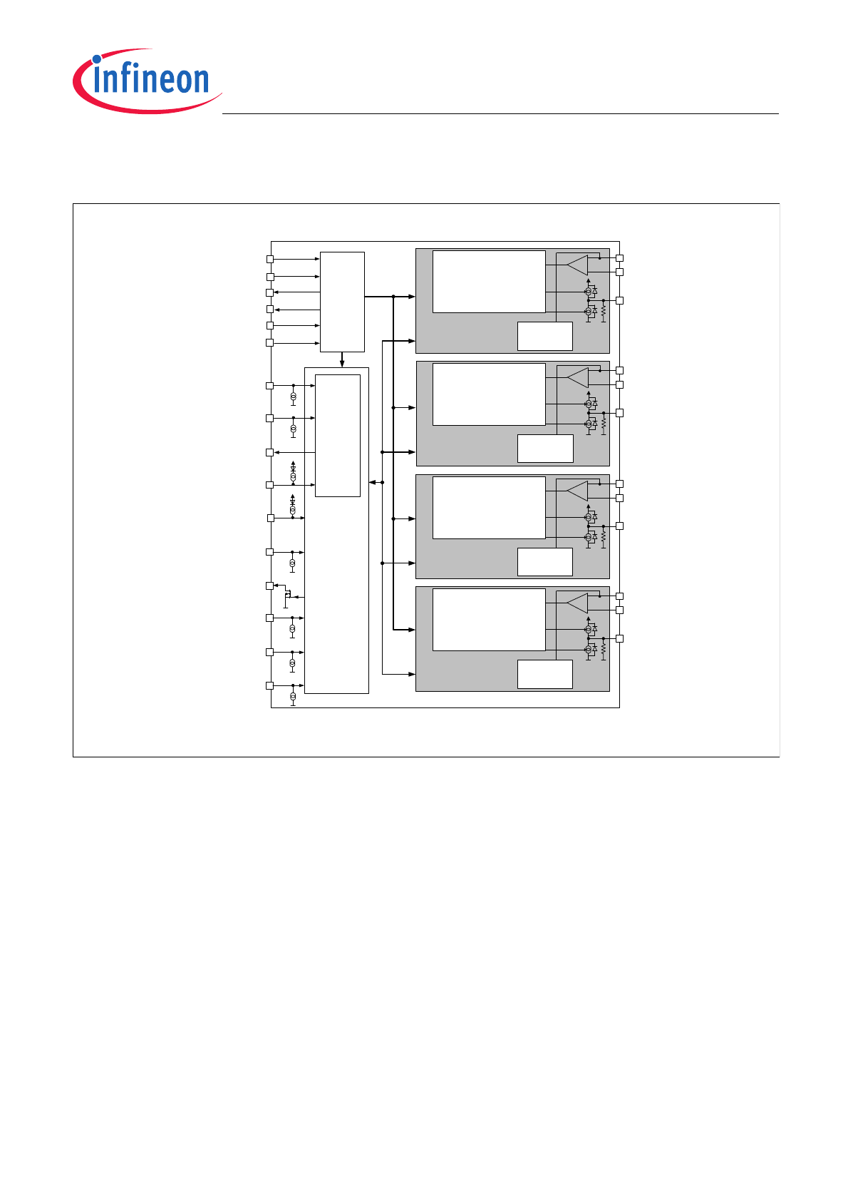
TLE7242-2G
Block Diagram
2
Block Diagram
Figure 7
Block Diagram
POS0
OUT0
NEG0
POS1
OUT1
NEG1
POS2
OUT2
NEG2
POS3
OUT3
NEG3
SPI
Interface
SCK
SI
SO
CS_B
FAULT
RESET_B
BAT
PHASE_SYNC
V5D
V5A
GND_D
GND_A
CLK
ENABLE
V_SIGNAL
TEST
Supply
Biasing
Monitoring
Logic
V_SIGNAL
V_SIGNAL
Current
Control
Block
Diagnostics
V5D
Current
Control
Block
Diagnostics
V5D
Current
Control
Block
Diagnostics
V5D
Current
Control
Block
Diagnostics
V5D
TLE7242-2G
Pin Configuration
Data Sheet
10
Rev. 1.1, 2011-05-27
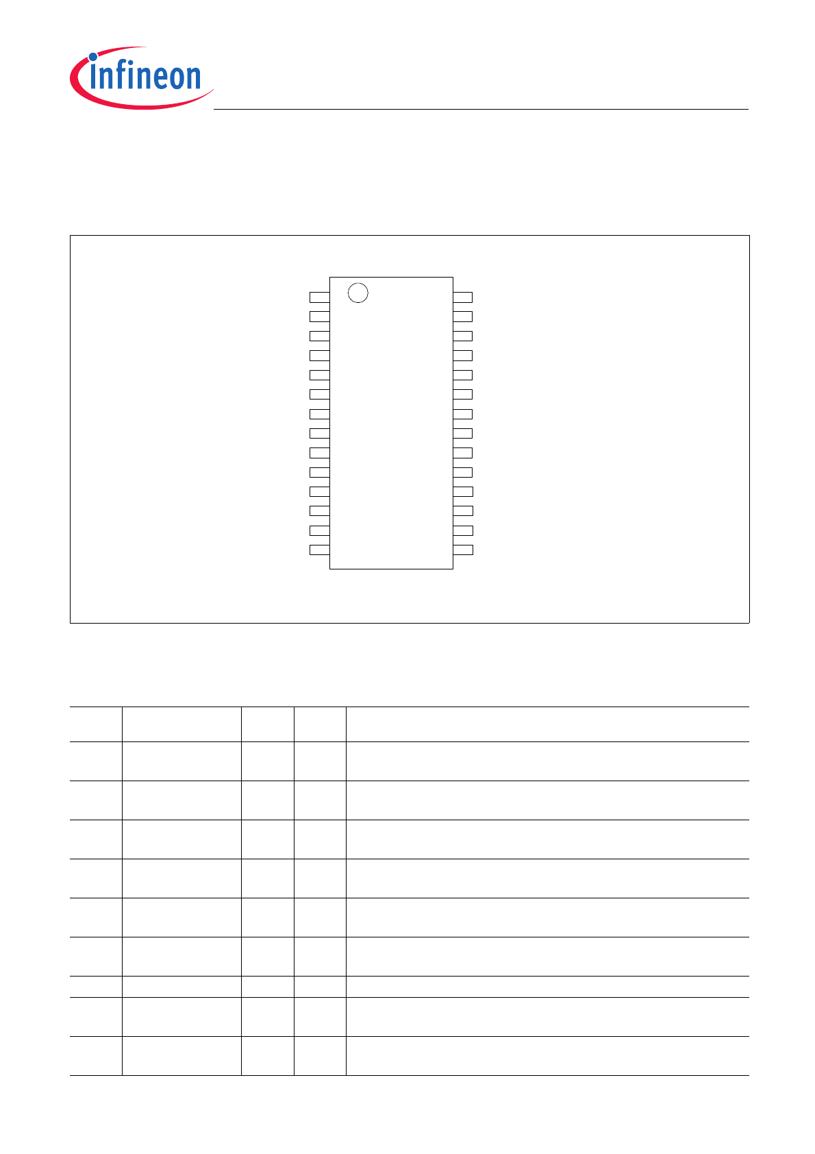
3
Pin Configuration
3.1
Pin Assignment
Figure 8
Pin Configuration
3.2
Pin Definitions and Functions
Pin
Symbol
I/O
Analog
/Digital
Function
1
OUT3
O
A
Gate driver output for channel #3. Connect to the gate of the
external MOSFET.
2
OUT2
O
A
Gate driver output for channel #2. Connect to the gate of the
external MOSFET.
3
POS3
I
A
Channel #3 Positive sense pin. Connect to the "load" side of the
external sense resistor.
4
NEG3
I
A
Channel #3 Negative sense pin. Connect to the "FET" side of the
external sense resistor.
5
NEG2
I
A
Channel #2 Negative sense pin. Connect to the "FET" side of the
external sense resistor.
6
POS2
I
A
Channel #2 Positive sense pin. Connect to the "load" side of the
external sense resistor.
7
GND_A
-
-
Analog Ground
8
V5A
-
-
5V supply pin for analog. An external capacitor is to be connected
between this pin and GND_A near this pin.
9
POS1
I
A
Channel #1 Positive sense pin. Connect to the "load" side of the
external sense resistor.
TLE724
2 2G
OUT 3
OUT 2
NEG 3
POS 3
FAULT
RESET_B
CS_B
ENABLE
NEG 2
POS 2
V5A
GND_A
SCK
V5D
GND_D
CLK
SO
V_SIGNAL
TEST
SI
PHASE_SYNC
BAT
NEG 1
POS 1
NEG 0
POS 0
OUT 1
OUT 0
1
2
3
4
5
6
7
8
9
10
11
12
13
14
28
27
26
25
24
23
22
21
20
19
18
17
16
15